64f29babbca0343aad4e5c8aa215fa91.ppt
- Количество слайдов: 25
 Click to edit Master Update: Summer Internship Progress title style Analysis and Modeling of Neural-Recording ADC Vaibhav Karkare Mentors: Wolfgang Eberle Vito Giannini
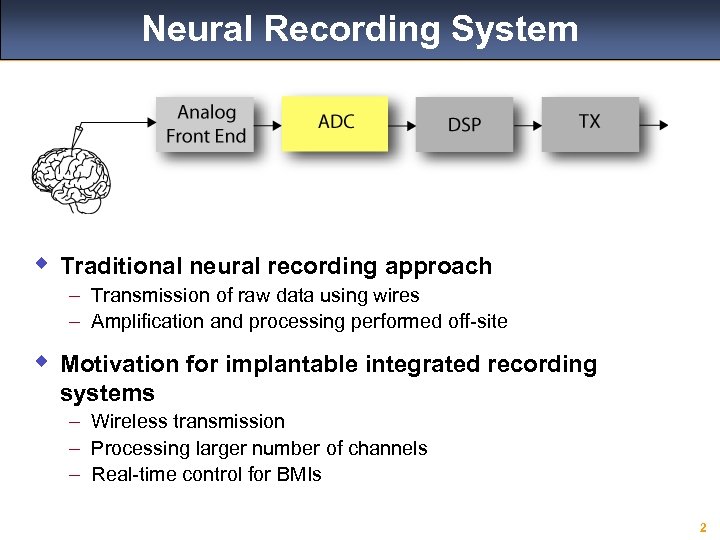 Neural Recording System w Traditional neural recording approach – Transmission of raw data using wires – Amplification and processing performed off-site w Motivation for implantable integrated recording systems – Wireless transmission – Processing larger number of channels – Real-time control for BMIs 2
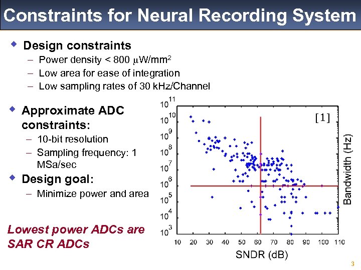 Constraints for Neural Recording System w Design constraints – Power density < 800 m. W/mm 2 – Low area for ease of integration – Low sampling rates of 30 k. Hz/Channel w Approximate ADC constraints: [1] – 10 -bit resolution – Sampling frequency: 1 MSa/sec w Design goal: – Minimize power and area Lowest power ADCs are SAR CR ADCs 3
![Notation for Non-Idealities of ADC Static error definitions for a ADC [2] 4 Notation for Non-Idealities of ADC Static error definitions for a ADC [2] 4](https://present5.com/presentation/64f29babbca0343aad4e5c8aa215fa91/image-4.jpg) Notation for Non-Idealities of ADC Static error definitions for a ADC [2] 4
Notation for Non-Idealities of ADC Static error definitions for a ADC [2] 4
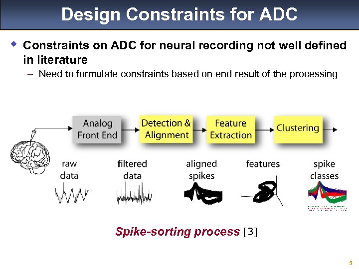 Design Constraints for ADC w Constraints on ADC for neural recording not well defined in literature – Need to formulate constraints based on end result of the processing Spike-sorting process [3] 5
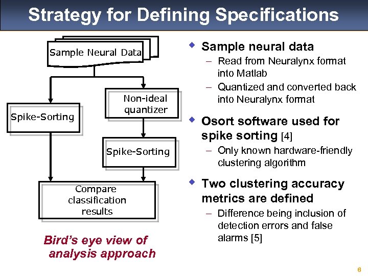 Strategy for Defining Specifications Sample Neural Data Spike-Sorting Non-ideal quantizer w Sample neural data – Read from Neuralynx format into Matlab – Quantized and converted back into Neuralynx format w Osort software used for spike sorting [4] Spike-Sorting Compare classification results Bird’s eye view of analysis approach – Only known hardware-friendly clustering algorithm w Two clustering accuracy metrics are defined – Difference being inclusion of detection errors and false alarms [5] 6
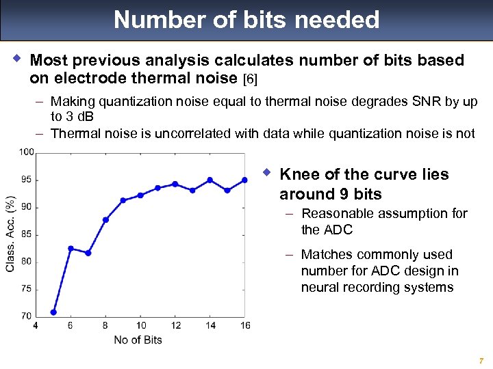 Number of bits needed w Most previous analysis calculates number of bits based on electrode thermal noise [6] – Making quantization noise equal to thermal noise degrades SNR by up to 3 d. B – Thermal noise is uncorrelated with data while quantization noise is not w Knee of the curve lies around 9 bits – Reasonable assumption for the ADC – Matches commonly used number for ADC design in neural recording systems 7
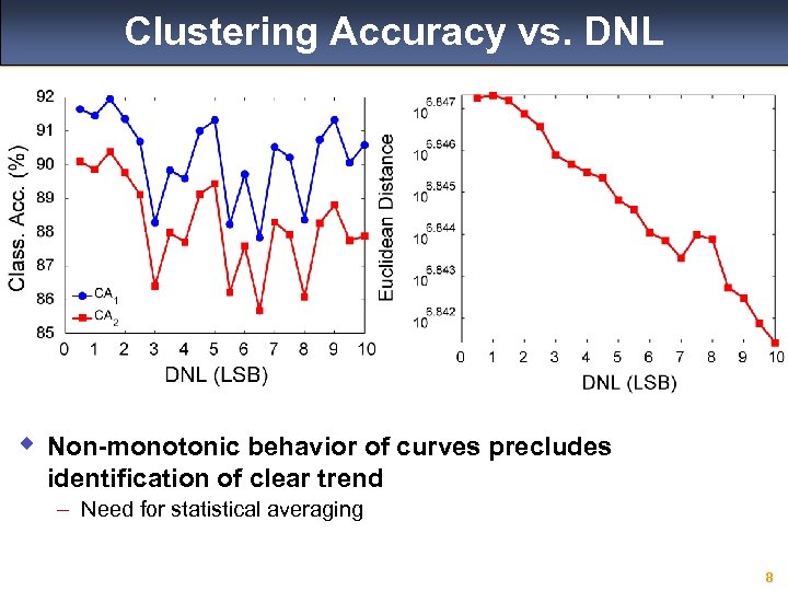 Clustering Accuracy vs. DNL w Non-monotonic behavior of curves precludes identification of clear trend – Need for statistical averaging 8
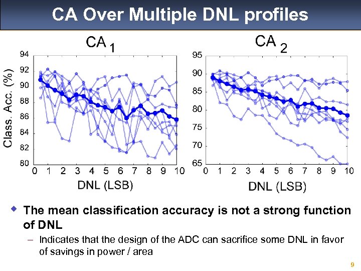 CA Over Multiple DNL profiles w The mean classification accuracy is not a strong function of DNL – Indicates that the design of the ADC can sacrifice some DNL in favor of savings in power / area 9
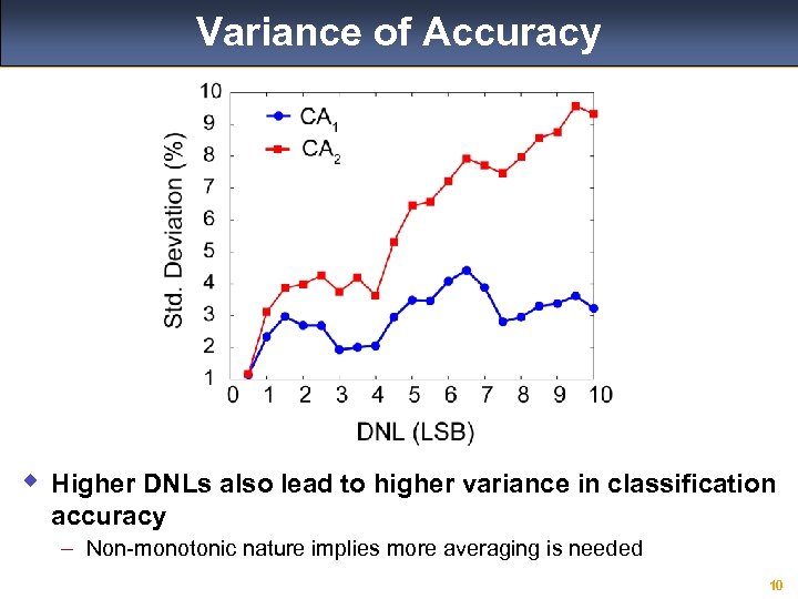 Variance of Accuracy w Higher DNLs also lead to higher variance in classification accuracy – Non-monotonic nature implies more averaging is needed 10
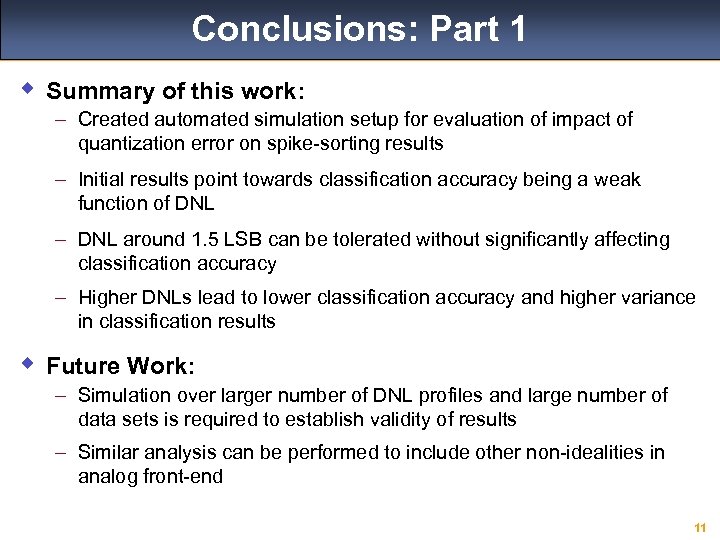 Conclusions: Part 1 w Summary of this work: – Created automated simulation setup for evaluation of impact of quantization error on spike-sorting results – Initial results point towards classification accuracy being a weak function of DNL – DNL around 1. 5 LSB can be tolerated without significantly affecting classification accuracy – Higher DNLs lead to lower classification accuracy and higher variance in classification results w Future Work: – Simulation over larger number of DNL profiles and large number of data sets is required to establish validity of results – Similar analysis can be performed to include other non-idealities in analog front-end 11
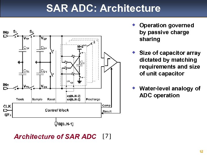 SAR ADC: Architecture w Operation governed by passive charge sharing w Size of capacitor array dictated by matching requirements and size of unit capacitor w Water-level analogy of ADC operation Architecture of SAR ADC [7] 12
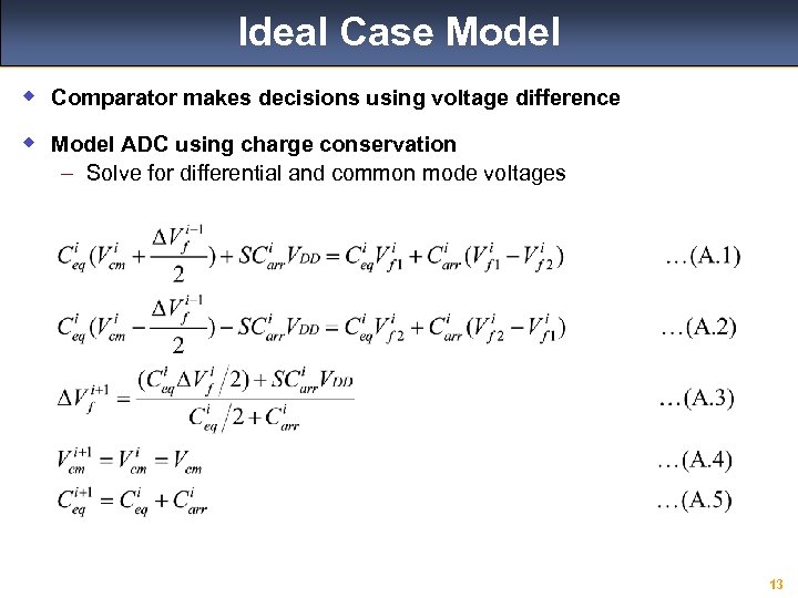 Ideal Case Model w Comparator makes decisions using voltage difference w Model ADC using charge conservation – Solve for differential and common mode voltages 13
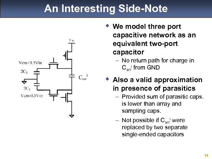 An Interesting Side-Note w We model three port capacitive network as an equivalent two-port capacitor – No return path for charge in Carri from GND w Also a valid approximation in presence of parasitics – Provided sum of parasitic caps. is lower than array and sampling caps. – Not possible if Carri were replaced by two separate single-ended capacitors 14
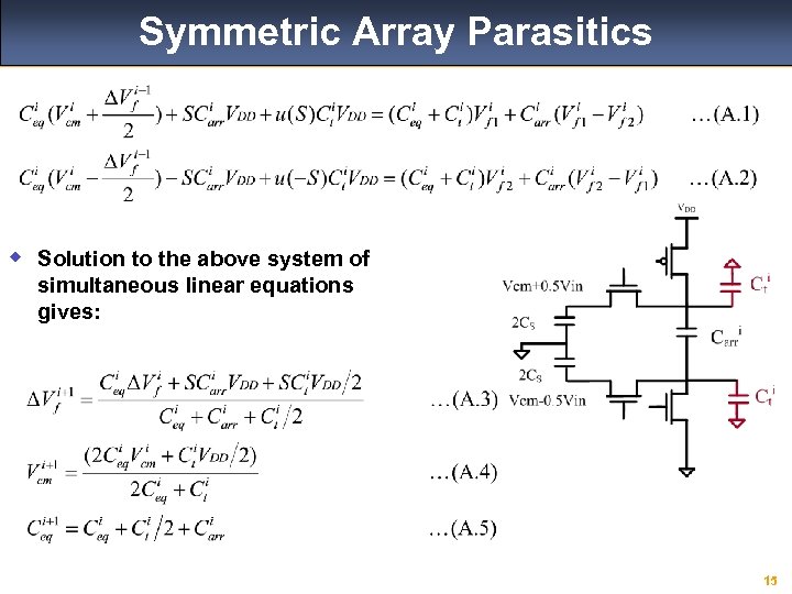 Symmetric Array Parasitics w Solution to the above system of simultaneous linear equations gives: 15
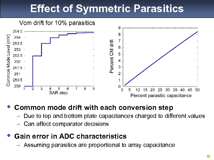 Effect of Symmetric Parasitics w Common mode drift with each conversion step – Due to top and bottom plate capacitances charged to different values – Can affect comparator decisions w Gain error in ADC characteristics – Assuming parasitics are proportional to array capacitance 16
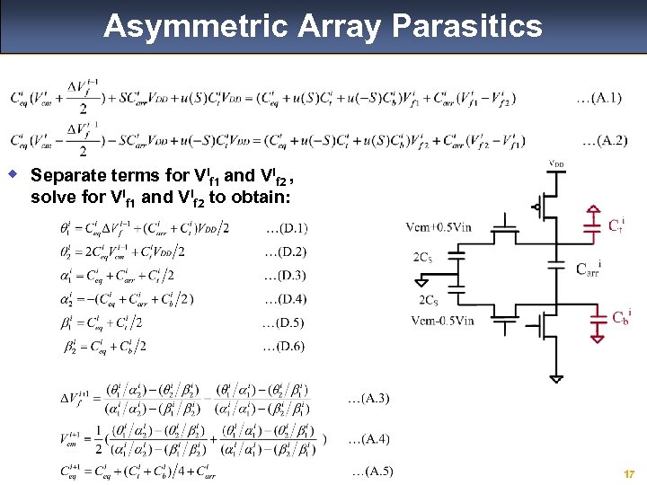 Asymmetric Array Parasitics w Separate terms for Vif 1 and Vif 2 , solve for Vif 1 and Vif 2 to obtain: 17
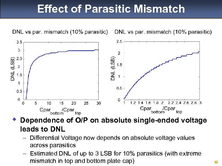 Effect of Parasitic Mismatch w Dependence of O/P on absolute single-ended voltage leads to DNL – Differential Voltage now depends on absolute voltage values across parasitics – Estimated DNL of up to 3 LSB for 10% parasitics (with extreme mismatch in top and bottom plate cap) 18
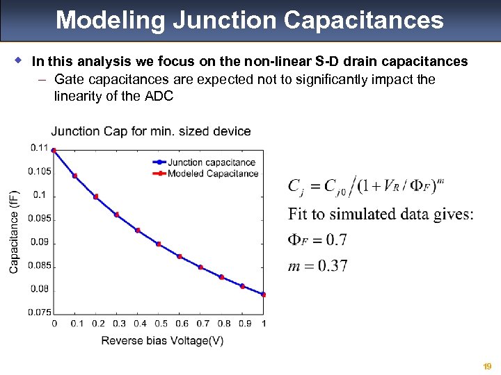 Modeling Junction Capacitances w In this analysis we focus on the non-linear S-D drain capacitances – Gate capacitances are expected not to significantly impact the linearity of the ADC 19
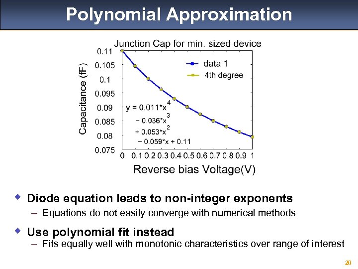 Polynomial Approximation w Diode equation leads to non-integer exponents – Equations do not easily converge with numerical methods w Use polynomial fit instead – Fits equally well with monotonic characteristics over range of interest 20
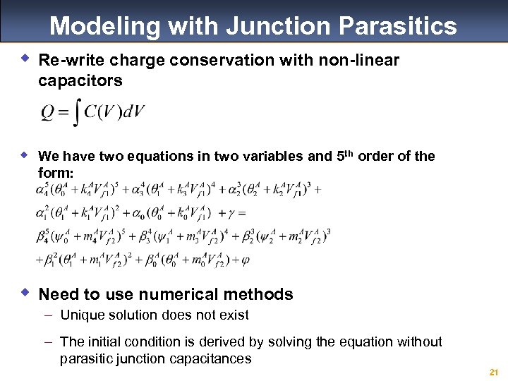 Modeling with Junction Parasitics w Re-write charge conservation with non-linear capacitors w We have two equations in two variables and 5 th order of the form: w Need to use numerical methods – Unique solution does not exist – The initial condition is derived by solving the equation without parasitic junction capacitances 21
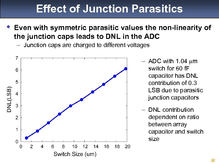 Effect of Junction Parasitics w Even with symmetric parasitic values the non-linearity of the junction caps leads to DNL in the ADC – Junction caps are charged to different voltages – ADC with 1. 04 mm switch for 60 f. F capacitor has DNL contribution of 0. 3 LSB due to parasitic junction capacitors – DNL contribution dependent on ratio between array capacitor and switch size 22
 Conclusions: Part 2 w Summary of this work: – Modeled the effect of non-linearities on static characteristics of ADC – Matlab model integrated with existing model which also includes comparator mismatch and thermal noise – Parasitics of array capacitance lead to a CM drift – Mismatch in parasitic capacitances leads to DNL – Junction capacitances lead to DNL even when switches are perfectly symmetric w Future Work: – Validation of model with Cadence simulations – Modeling dynamic non-idealities of ADC – Combining Part 1 and Part 2 to have a application-specific optimized ADC – Check out for options to better performance of previous ADC using trends shown by models 23
![References/Acknowledgments REFERENCES [1] B. Murmann, “ADC Performance Survey 1997 -2009”, [Online] Available: http: //www. References/Acknowledgments REFERENCES [1] B. Murmann, “ADC Performance Survey 1997 -2009”, [Online] Available: http: //www.](https://present5.com/presentation/64f29babbca0343aad4e5c8aa215fa91/image-24.jpg) References/Acknowledgments REFERENCES [1] B. Murmann, “ADC Performance Survey 1997 -2009”, [Online] Available: http: //www. stanford. edu/~murmann/adcsurvey. html [2] B. Razavi, “Principles of Data Conversion System Design”, IEEE Press, 2005 [3] V. Karkare, S. Gibson, and D. Markovic, “A 130 m. W, 64 -Channel Spike-Sorting DSP Chip”, ASSCC, Nov’ 09 [4] U. Reutishauser, E. Schuman, and A. Mamelak, “Online detection and sorting of extracellularly recorded action potentials in human medial temporal lobe recordings in vivo”, JNM, May’ 05 [5] S. Gibson, J. W. Judy, and D. Markovic, “Comparison of Spike-Sorting Algorithms for Future Hardware Implementation”, EMBC, Aug’ 08 [6] M. Chae, et. al. , “Design Optimization for Integrated Neural Recording Systems”, JSSC, Sep’ 08 [7] J. Craininckx and G. Van der Plaas, “A 65 f. J/Conversion-Step 0 -to-50 MS/s 0 -to 0. 7 m. W 9 b Charge Sharing SAR ADC in 90 nm Digital CMOS”, ISSCC, Feb’ 07 ACKNOWLEDGMENTS Wolfgang Eberle, Vito Gianniani, Dejan Markovic, Sarah Gibson, and Ivan Gligorijevic. 24
References/Acknowledgments REFERENCES [1] B. Murmann, “ADC Performance Survey 1997 -2009”, [Online] Available: http: //www. stanford. edu/~murmann/adcsurvey. html [2] B. Razavi, “Principles of Data Conversion System Design”, IEEE Press, 2005 [3] V. Karkare, S. Gibson, and D. Markovic, “A 130 m. W, 64 -Channel Spike-Sorting DSP Chip”, ASSCC, Nov’ 09 [4] U. Reutishauser, E. Schuman, and A. Mamelak, “Online detection and sorting of extracellularly recorded action potentials in human medial temporal lobe recordings in vivo”, JNM, May’ 05 [5] S. Gibson, J. W. Judy, and D. Markovic, “Comparison of Spike-Sorting Algorithms for Future Hardware Implementation”, EMBC, Aug’ 08 [6] M. Chae, et. al. , “Design Optimization for Integrated Neural Recording Systems”, JSSC, Sep’ 08 [7] J. Craininckx and G. Van der Plaas, “A 65 f. J/Conversion-Step 0 -to-50 MS/s 0 -to 0. 7 m. W 9 b Charge Sharing SAR ADC in 90 nm Digital CMOS”, ISSCC, Feb’ 07 ACKNOWLEDGMENTS Wolfgang Eberle, Vito Gianniani, Dejan Markovic, Sarah Gibson, and Ivan Gligorijevic. 24
 Questions / Comments? 25


