b4827c50ea66570c7f24b57f72a7c68d.ppt
- Количество слайдов: 27
 CLIC Workshop 2013 CERN Sensor R&D at CNM G. Pellegrini Centro Nacional de Microelectrónica (IMB-CNM-CSIC) Barcelona, Spain G. Pellegrini 1
 CLIC Workshop 2013 CERN Outline • -CNM facilities • Ultra fast silicon detectors with charge multiplication • New 2 D position sensitive microstrip detectors • Conclusions G. Pellegrini 2
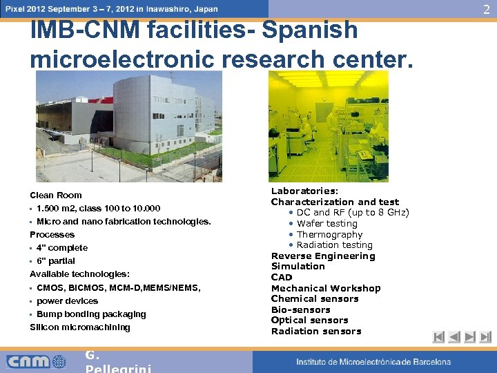 CLIC Workshop 2013 CERN IMB-CNM facilities- Spanish microelectronic research center. Clean Room • 1. 500 m 2, class 100 to 10. 000 • Micro and nano fabrication technologies. Processes • 4'' complete • 6'' partial Available technologies: • CMOS, Bi. CMOS, MCM-D, MEMS/NEMS, • power devices • Bump bonding packaging Silicon micromachining G. G. Pellegrini Laboratories: Characterization and test • DC and RF (up to 8 GHz) • Wafer testing • Thermography • Radiation testing Reverse Engineering Simulation CAD Mechanical Workshop Chemical sensors Bio-sensors Optical sensors Radiation sensors 2 3
 4 CLIC Workshop 2013 CERN Charge Multiplication- pixel detectors We are starting the fabrication of new p-type pixel detectors with enhanced multiplication effect in the n-type electrodes, very low collection times and with no cross-talk. 3 different approaches: 1. Thin p-type epitaxyal substrates 2. Low gain avalanche detectors 3. 3 D with enhanced electric field. Planar- Same mask Two projects funded by CERN RD 50 collaboration to work on these technologies. http: //rd 50. web. cern. ch/rd 50/ G. Pellegrini
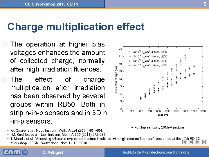 CLIC Workshop 2013 CERN Charge multiplication effect p p The operation at higher bias voltages enhances the amount of collected charge, normally after high irradiation fluences. The effect of charge multiplication after irradiation has been observed by several groups within RD 50. Both in strip n-in-p sensors and in 3 D n -in-p sensors. n-in-p strip sensors, 26 Me. V protons. • G. Casse, et al, Nucl. Instrum. Meth. A 624 (2011) 401 -404. • M. Koehler, et al, Nucl. Instrum. Meth. A 659 (2011) 272 -281. • I. Mandic et al, “Annealing effects in n+p strip detectors irradiated with high neutron fluences”, presented at the 17 th RD 50 Workshop, CERN, Switzerland, Nov. 17 -19, 2010 G. Pellegrini 5
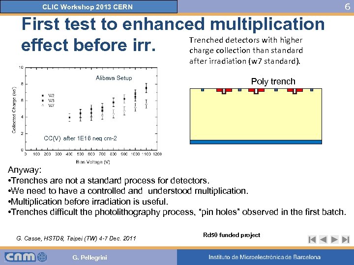 6 CLIC Workshop 2013 CERN First test to enhanced multiplication Trenched detectors with higher effect before irr. charge collection than standard after irradiation (w 7 standard). Alibava Setup Poly trench CC(V) after 1 E 16 neq cm-2 Anyway: • Trenches are not a standard process for detectors. • We need to have a controlled and understood multiplication. • Multiplication before irradiation is useful. • Trenches difficult the photolithography process, “pin holes” observed in the first batch. G. Casse, HSTD 8, Taipei (TW) 4 -7 Dec. 2011 G. Pellegrini Rd 50 funded project
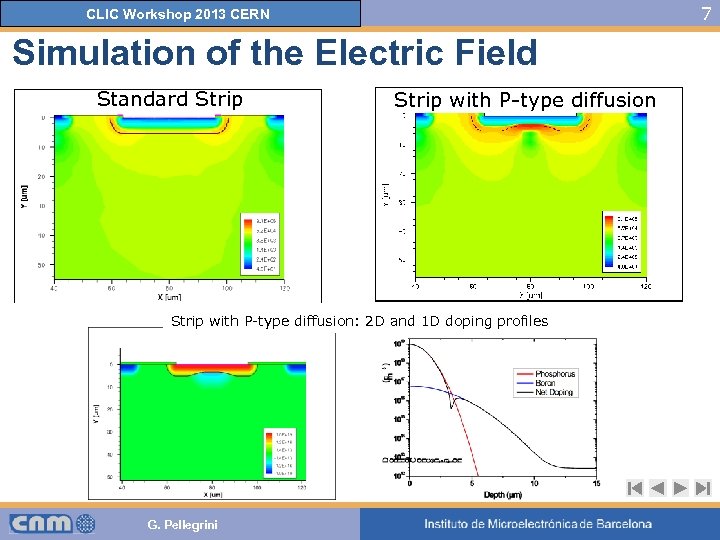 7 CLIC Workshop 2013 CERN Simulation of the Electric Field Standard Strip with P-type diffusion: 2 D and 1 D doping profiles G. Pellegrini
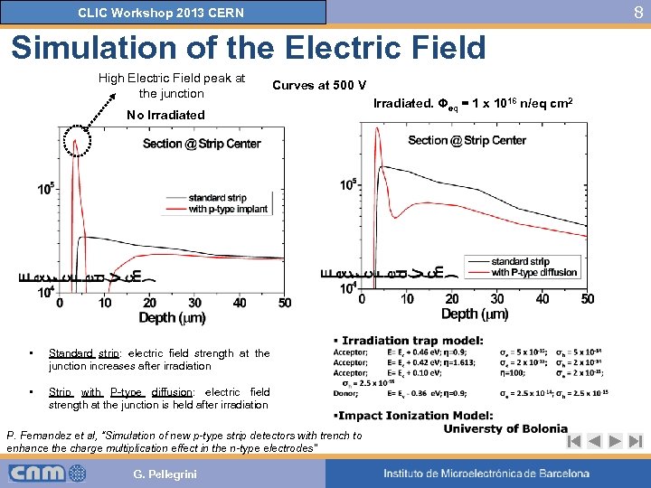 8 CLIC Workshop 2013 CERN Simulation of the Electric Field High Electric Field peak at the junction Curves at 500 V No Irradiated • Standard strip: electric field strength at the junction increases after irradiation • Strip with P-type diffusion: electric field strength at the junction is held after irradiation P. Fernandez et al, “Simulation of new p-type strip detectors with trench to enhance the charge multiplication effect in the n-type electrodes” G. Pellegrini Irradiated. Φeq = 1 x 10¹⁶ n/eq cm 2
 CLIC Workshop 2013 CERN Fabrication of new p-type pixel detectors with enhanced multiplication effect in the n-type electrodes. RD 50 Institutes participating in these project: CNM-Barcelona, G. Pellegrini, Giulio. Pellegrini@cnm-imb. csic. es Liverpool University, Gianluigi Casse, gcasse@hep. ph. liv. ac. uk UC Santa Cruz, Hartmut Sadrozinki, hartmut@ucsc. edu IFAE, Barcelona, Sebastian Grinstein, sgrinstein@ifae. es KIT, Karlsruhe, Prof. Wim de Bôer, wim. de. boer@kit. edu IFCA Santander, Ivan Vila, ivan. vila@csic. es University of Glasgow, Richard Bates, richard. bates@glasgow. ac. uk INFN Florence, Mara Bruzzi, mara. bruzzi@unifi. it CERN, M. Moll, Michael. Moll@cern. ch G. Pellegrini 9
 CLIC Workshop 2013 CERN 1)Thin p-type epitaxyal substrates Detector proposed by Hartmut Sadrozinski and Abe Seiden (UCSC) , Ultra-Fast Silicon Detectors (UFSD). Provide in the same detector and readout chain • Ultra-fast timing resolution [10’s of ps] • Precision location information [10’s of µm] We propose to achieve high electric field is to use thin p-type epitaxyal substrates [1] grown on thick support wafers, p+-type doped, that acts as the backside ohmic contact. Different thicknesses will be used to study the multiplication effect induced by the high electric field at the collecting electrodes, depending on availability we propose to use: 10, 50, 75µm. Need very fast pixel readout. H. Sadrozinski, “Exploring charge multiplication for fast timing with silicon sensors” 20 th RD 50 Workshop, Bari 2012 G. Pellegrini 10
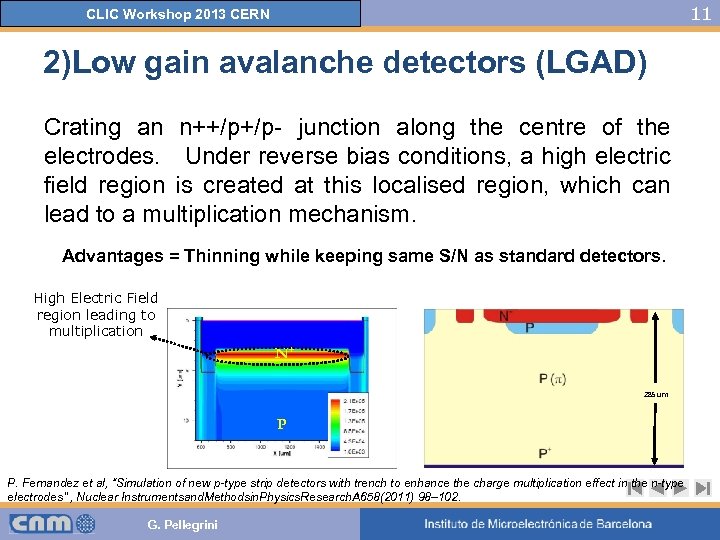 11 CLIC Workshop 2013 CERN 2)Low gain avalanche detectors (LGAD) Crating an n++/p+/p- junction along the centre of the electrodes. Under reverse bias conditions, a high electric field region is created at this localised region, which can lead to a multiplication mechanism. Advantages = Thinning while keeping same S/N as standard detectors. High Electric Field region leading to multiplication N+ 285 um P P. Fernandez et al, “Simulation of new p-type strip detectors with trench to enhance the charge multiplication effect in the n-type electrodes” , Nuclear Instrumentsand. Methodsin. Physics. Research. A 658(2011) 98– 102. G. Pellegrini
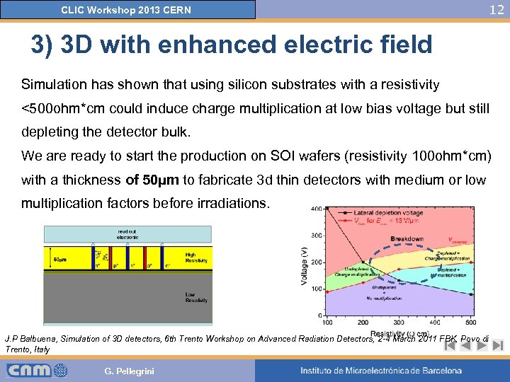 CLIC Workshop 2013 CERN 12 3) 3 D with enhanced electric field Simulation has shown that using silicon substrates with a resistivity <500 ohm*cm could induce charge multiplication at low bias voltage but still depleting the detector bulk. We are ready to start the production on SOI wafers (resistivity 100 ohm*cm) with a thickness of 50µm to fabricate 3 d thin detectors with medium or low multiplication factors before irradiations. J. P Balbuena, Simulation of 3 D detectors, 6 th Trento Workshop on Advanced Radiation Detectors, 2 -4 March 2011 FBK, Povo di Trento, Italy G. Pellegrini
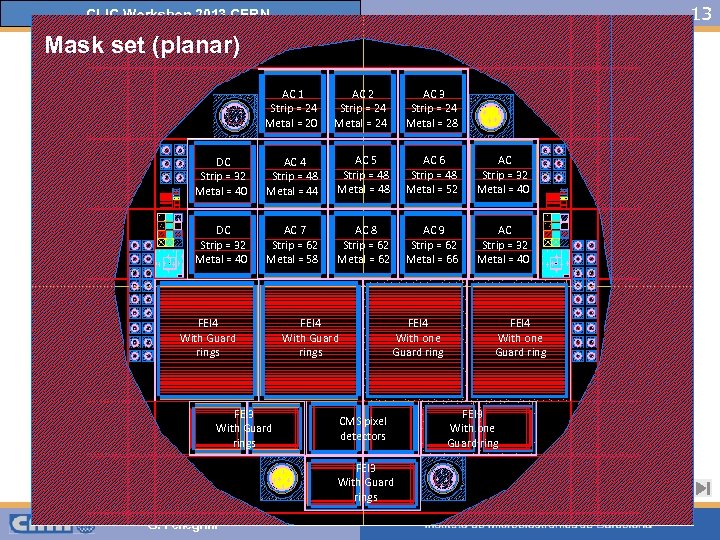 13 CLIC Workshop 2013 CERN Mask set (planar) AC 1 Strip = 24 Metal = 20 AC 2 Strip = 24 Metal = 24 AC 3 Strip = 24 Metal = 28 DC Strip = 32 Metal = 40 AC 4 Strip = 48 Metal = 44 AC 5 Strip = 48 Metal = 48 AC 6 Strip = 48 Metal = 52 AC Strip = 32 Metal = 40 DC Strip = 32 Metal = 40 AC 7 Strip = 62 Metal = 58 AC 8 Strip = 62 Metal = 62 AC 9 Strip = 62 Metal = 66 AC Strip = 32 Metal = 40 FEI 4 With Guard rings FEI 3 With Guard rings FEI 4 With one Guard ring CMS pixel detectors FEI 3 With Guard rings G. Pellegrini FEI 4 With one Guard ring FEI 3 With one Guard ring
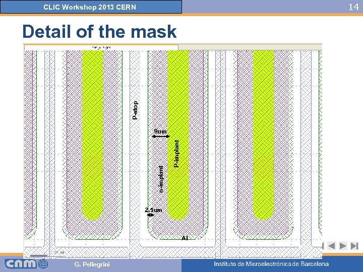 14 CLIC Workshop 2013 CERN P-stop Detail of the mask P-implant n-implant 9 um 2. 5 um Al G. Pellegrini
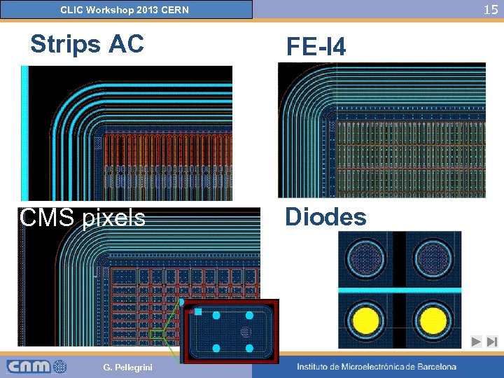 15 CLIC Workshop 2013 CERN Strips AC CMS pixels G. Pellegrini FE-I 4 Diodes
![16 CLIC Workshop 2013 CERN Strip detectors Pitch p=80 mm Strip w [mm] Metal 16 CLIC Workshop 2013 CERN Strip detectors Pitch p=80 mm Strip w [mm] Metal](https://present5.com/presentation/b4827c50ea66570c7f24b57f72a7c68d/image-16.jpg) 16 CLIC Workshop 2013 CERN Strip detectors Pitch p=80 mm Strip w [mm] Metal [mm] P-implant [mm] w/p AC 1 24 20 6 0. 3 AC 2 24 24 6 0. 3 AC 3 24 28 6 0. 3 AC 4 48 44 30 0. 6 AC 5 48 48 30 0. 6 AC 6 48 52 30 0. 6 AC 7 62 58 44 0. 775 AC 8 62 62 44 0. 775 AC 9 62 66 44 0. 775 AC and DC 32 40 14 0. 4 G. Pellegrini
16 CLIC Workshop 2013 CERN Strip detectors Pitch p=80 mm Strip w [mm] Metal [mm] P-implant [mm] w/p AC 1 24 20 6 0. 3 AC 2 24 24 6 0. 3 AC 3 24 28 6 0. 3 AC 4 48 44 30 0. 6 AC 5 48 48 30 0. 6 AC 6 48 52 30 0. 6 AC 7 62 58 44 0. 775 AC 8 62 62 44 0. 775 AC 9 62 66 44 0. 775 AC and DC 32 40 14 0. 4 G. Pellegrini
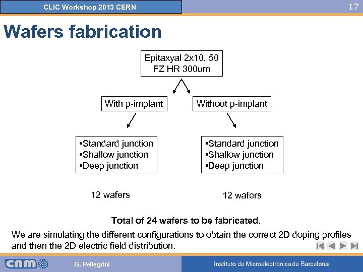 17 CLIC Workshop 2013 CERN Wafers fabrication Epitaxyal 2 x 10, 50 FZ HR 300 um With p-implant • Standard junction • Shallow junction • Deep junction 12 wafers Without p-implant • Standard junction • Shallow junction • Deep junction 12 wafers Total of 24 wafers to be fabricated. We are simulating the different configurations to obtain the correct 2 D doping profiles and then the 2 D electric field distribution. G. Pellegrini
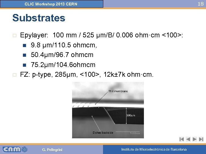 CLIC Workshop 2013 CERN Substrates p p Epylayer: 100 mm / 525 µm/B/ 0. 006 ohm·cm <100>: n 9. 8 µm/110. 5 ohmcm, n 50. 4µm/96. 7 ohmcm n 75. 2µm/104. 6 ohmcm FZ: p-type, 285µm, <100>, 12 k± 7 k ohm·cm. G. Pellegrini 18
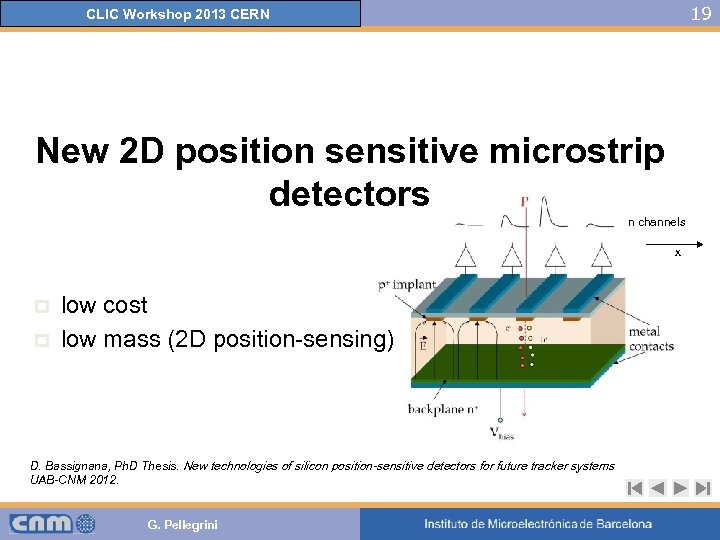 19 CLIC Workshop 2013 CERN New 2 D position sensitive microstrip detectors n channels x p p low cost low mass (2 D position-sensing) D. Bassignana, Ph. D Thesis. New technologies of silicon position-sensitive detectors for future tracker systems UAB-CNM 2012. G. Pellegrini
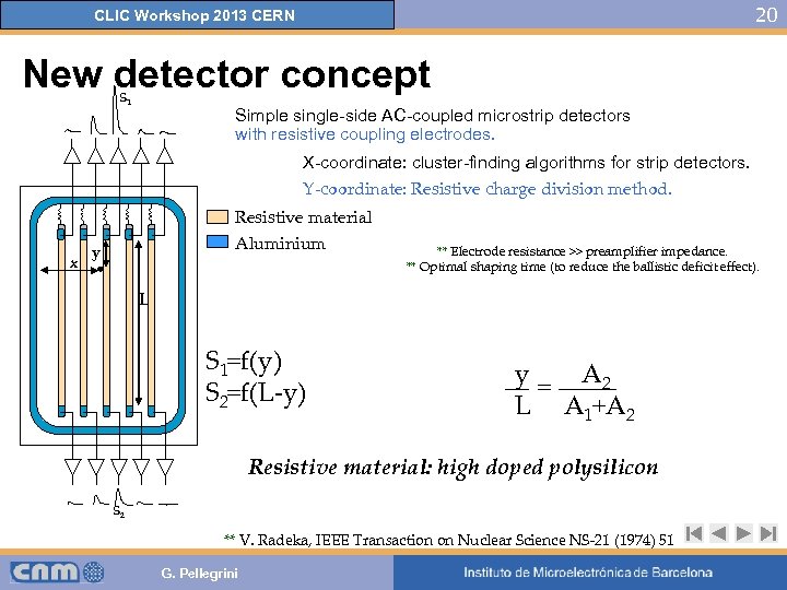 20 CLIC Workshop 2013 CERN New detector concept S 1 Simple single-side AC-coupled microstrip detectors with resistive coupling electrodes. X-coordinate: cluster-finding algorithms for strip detectors. Y-coordinate: Resistive charge division method. x Resistive material Aluminium y ** Electrode resistance >> preamplifier impedance. ** Optimal shaping time (to reduce the ballistic deficit effect). L S 1=f(y) S 2=f(L-y) y = A 2 L A 1+A 2 Resistive material: high doped polysilicon S 2 ** V. Radeka, IEEE Transaction on Nuclear Science NS-21 (1974) 51 G. Pellegrini
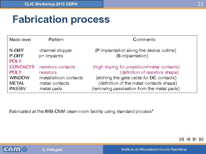 21 CLIC Workshop 2013 CERN Fabrication process Mask level N-DIFF POLY CONTACTS POLY WINDOW METAL PASSIV Pattern channel stopper p+ implants resistors contacts resistors metal/silicon contacts metal pads Comments (P implantation along the device cutline) (B implantation) (high doping for polysilicon/metal contacts) (definition of resistors shape) (etching the gate oxide for DC contacts) (definition of the metal contacts shape) (removing passivation from the metal pads) Fabricated at the IMB-CNM clean-room facility using standard process* G. Pellegrini
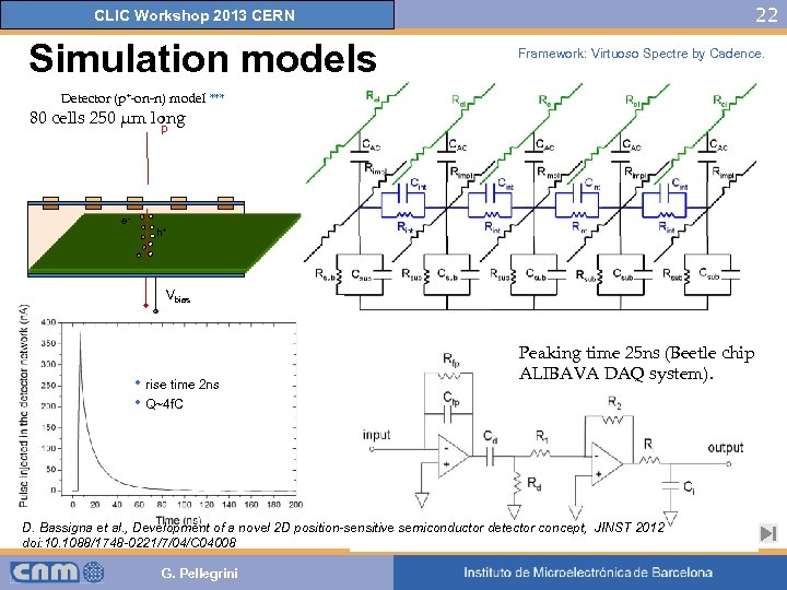 22 CLIC Workshop 2013 CERN Simulation models Framework: Virtuoso Spectre by Cadence. Detector (p+-on-n) model *** 80 cells 250 μm long p e- h+ Vbias • rise time 2 ns • Q~4 f. C Peaking time 25 ns (Beetle chip ALIBAVA DAQ system). D. Bassigna et al. , Development of a novel 2 D position-sensitive semiconductor detector concept, JINST 2012 doi: 10. 1088/1748 -0221/7/04/C 04008 G. Pellegrini
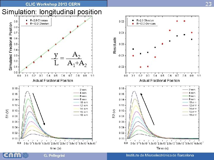 23 CLIC Workshop 2013 CERN Simulation: longitudinal position S 1 Particle t 1 t S 1 S 2 t 2 2 mm t y V y A 2 = L A 1+A 2 Short shaping time G. Pellegrini S 2 18 mm Non constant ballistic deficit (propagation length, Relectrode)
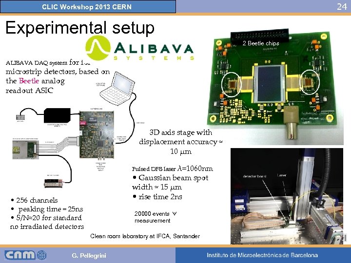 24 CLIC Workshop 2013 CERN Experimental setup 2 Beetle chips ALIBAVA DAQ system for microstrip detectors, based on the Beetle analog readout ASIC 3 D axis stage with displacement accuracy ≈ 10 μm Pulsed DFB laser λ=1060 nm • Gaussian beam spot width ≈ 15 μm • rise time 2 ns • 256 channels • peaking time = 25 ns • S/N≈20 for standard no irradiated detectors 20000 events ∀ measurement Clean room laboratory at IFCA, Santander G. Pellegrini
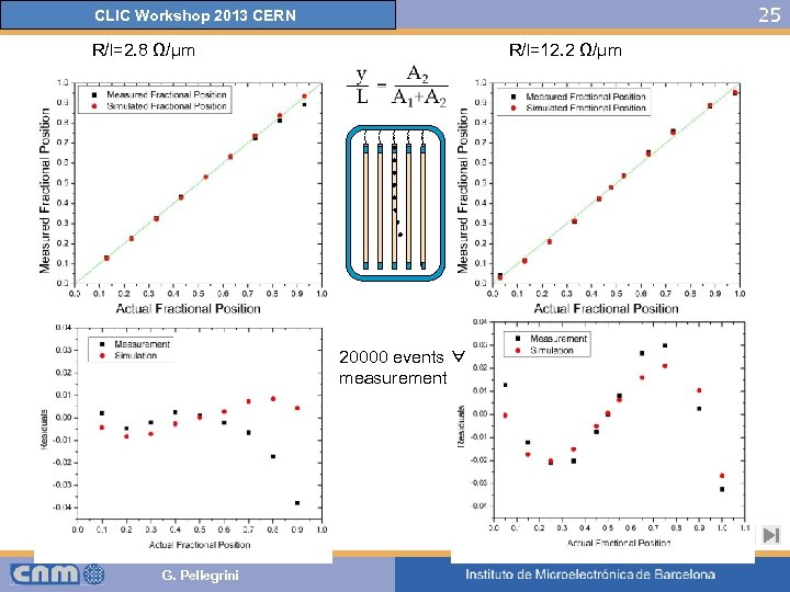 25 CLIC Workshop 2013 CERN R/l=2. 8 Ω/μm R/l=12. 2 Ω/μm 20000 events ∀ measurement Systematic error => Ballistic deficit G. Pellegrini
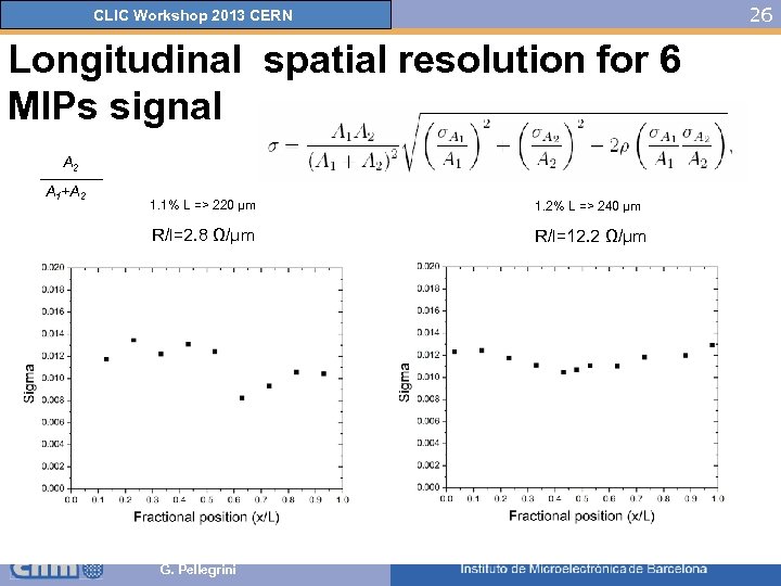 26 CLIC Workshop 2013 CERN Longitudinal spatial resolution for 6 MIPs signal A 2 A 1+A 2 1. 1% L => 220 μm 1. 2% L => 240 μm R/l=2. 8 Ω/μm R/l=12. 2 Ω/μm σA 1=1. 83 ADU G. Pellegrini σA 2=1. 80 ADU
 CLIC Workshop 2013 CERN Conclusions • • • The effect of charge multiplication has been observed within RD 50 and it was started to be investigated systematically. New detector designs aim to fabricate detectors with moderate gain and fast collection times. Single side microstrip detector 2 D position-sensitive with AC coupled resistive electrodes Combining different technologies will make the ideal detectors: thin, ultra fast, high S/N and 2 D with a low number of channels. G. Pellegrini 27


