d6295e938c88c1feee3957d1dc49858d.ppt
- Количество слайдов: 78
Chapter 7 Sequential Circuits Boonchuay Supmonchai Integrated Design Application Research (IDAR) Laboratory August 20, 2004; Revised - July 4, 2005 2102 -545 Digital ICs
B. Supmonchai Goals of This Chapter q Implementation techniques for § Register: latches and flipflops § Schmitt Triggers § Oscillator, pulse generators q Static versus Dynamic Realization q Clocking Strategies 2102 -545 Digital ICs Sequential Logic 2
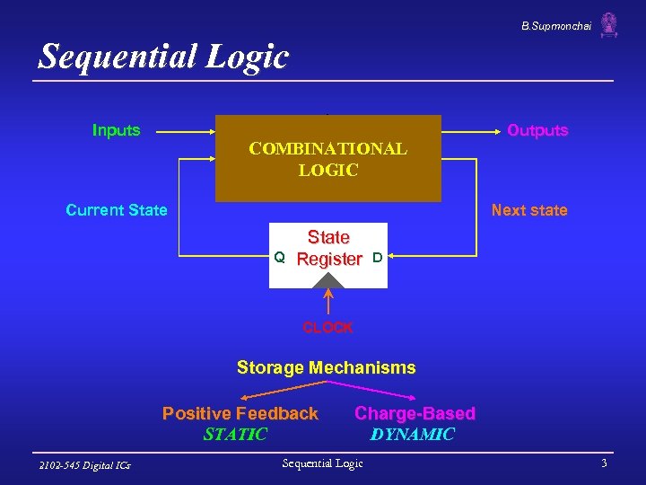
B. Supmonchai Sequential Logic Inputs COMBINATIONAL LOGIC Current State Outputs Next state Q State Register D CLOCK Storage Mechanisms Positive Feedback STATIC 2102 -545 Digital ICs Charge-Based DYNAMIC Sequential Logic 3
B. Supmonchai Static vs Dynamic Storage q Static storage § preserve state as long as the power is on § have positive feedback (regeneration) with an internal regeneration connection between the output and the input § useful when updates are infrequent (clock gating) q Dynamic storage § store state on parasitic capacitors § only hold state for short periods of time (milliseconds) § require periodic refresh § usually simpler, so higher speed and lower power 2102 -545 Digital ICs Sequential Logic 4
B. Supmonchai Latches versus Flipflops q Latches (with Clock) § level sensitive circuit that passes inputs to Q when the clock is high (or low) - transparent mode § input sampled on the falling edge of the clock is held stable when clock is low (or high) - hold mode q Flipflops (edge-triggered) § edge sensitive circuits that sample the inputs on a clock transition Ø positive edge-triggered: 0 1 Ø negative edge-triggered: 1 0 § built using latches (e. g. , master-slave flipflops) 2102 -545 Digital ICs Sequential Logic 5
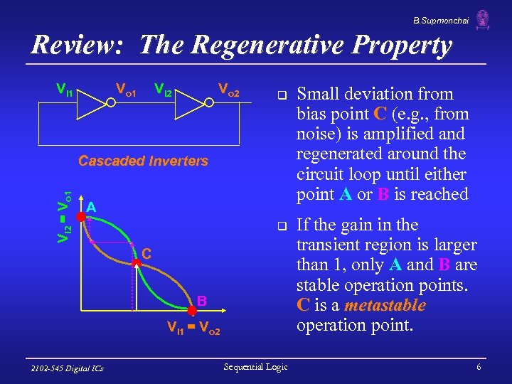
B. Supmonchai Review: The Regenerative Property Vi 1 Vo 1 Vi 2 Vo 2 q Vi 2 = Vo 1 Cascaded Inverters A q C B Vi 1 = Vo 2 2102 -545 Digital ICs Sequential Logic Small deviation from bias point C (e. g. , from noise) is amplified and regenerated around the circuit loop until either point A or B is reached If the gain in the transient region is larger than 1, only A and B are stable operation points. C is a metastable operation point. 6
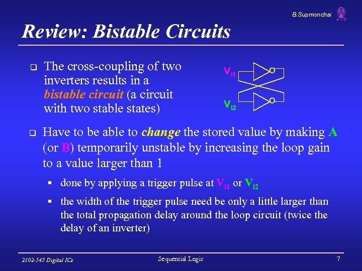
B. Supmonchai Review: Bistable Circuits q q The cross-coupling of two inverters results in a bistable circuit (a circuit with two stable states) Vi 1 Vi 2 Have to be able to change the stored value by making A (or B) temporarily unstable by increasing the loop gain to a value larger than 1 § done by applying a trigger pulse at Vi 1 or Vi 2 § the width of the trigger pulse need be only a little larger than the total propagation delay around the loop circuit (twice the delay of an inverter) 2102 -545 Digital ICs Sequential Logic 7
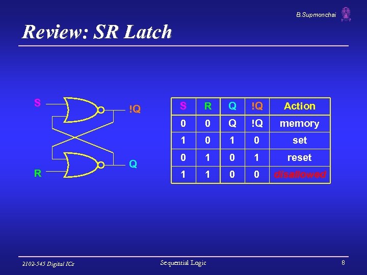
B. Supmonchai Review: SR Latch S R 2102 -545 Digital ICs R Q !Q Action 0 Q !Q memory 1 Q S 0 !Q 0 1 0 set 0 1 reset 1 1 0 0 disallowed Sequential Logic 8
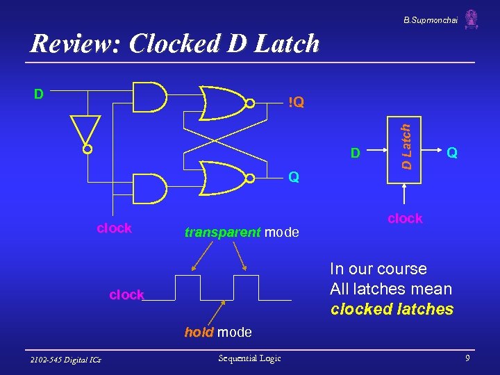
B. Supmonchai Review: Clocked D Latch D D Q clock transparent mode D Latch !Q Q clock In our course All latches mean clocked latches clock hold mode 2102 -545 Digital ICs Sequential Logic 9
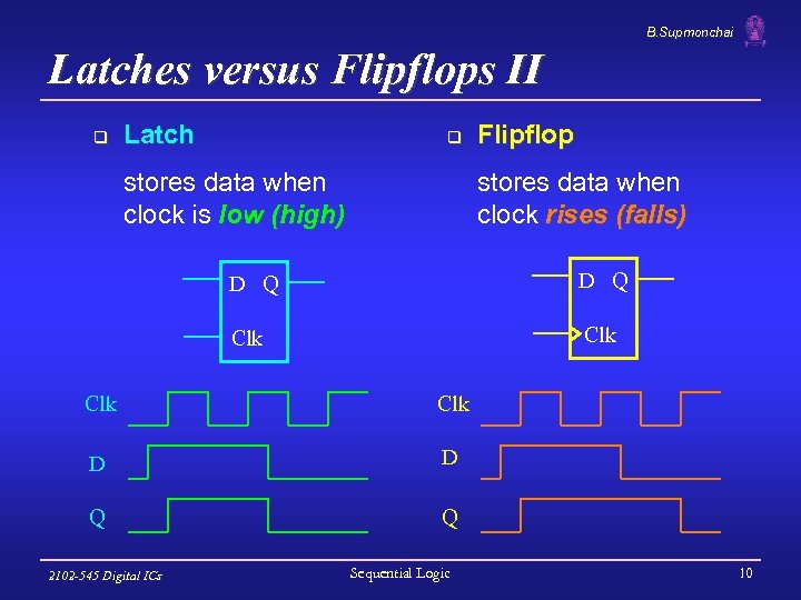
B. Supmonchai Latches versus Flipflops II q Latch q stores data when clock is low (high) Flipflop stores data when clock rises (falls) D Q Clk Clk D D Q Q 2102 -545 Digital ICs Sequential Logic 10
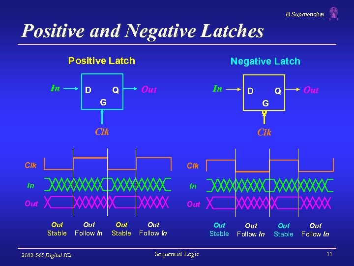
B. Supmonchai Positive and Negative Latches Positive Latch In D Q Negative Latch In Out Q D G Out Stable Out Follow In G Clk Out Clk Clk In In Out Out Stable 2102 -545 Digital ICs Out Follow In Out Stable Out Follow In Sequential Logic Out Stable Out Follow In 11
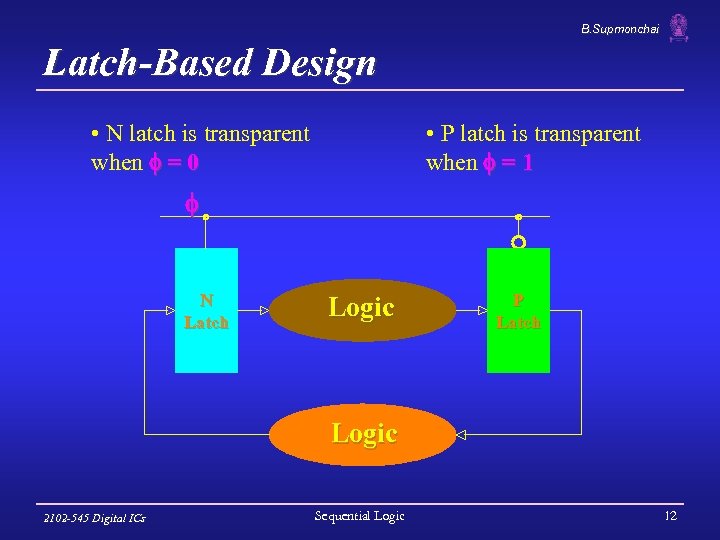
B. Supmonchai Latch-Based Design • N latch is transparent when f = 0 • P latch is transparent when f = 1 f N Latch Logic P Latch Logic 2102 -545 Digital ICs Sequential Logic 12
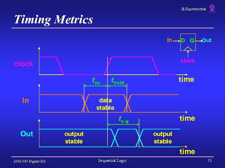
B. Supmonchai Timing Metrics In Out clock tsu In time thold data stable time tc-q Out D Q output stable time 2102 -545 Digital ICs Sequential Logic 13
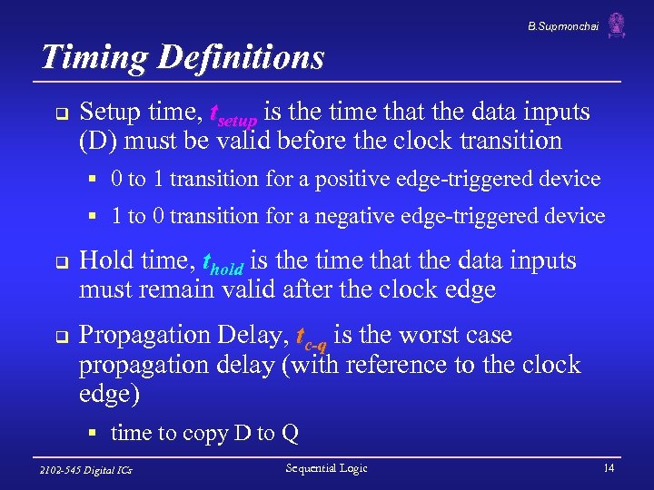
B. Supmonchai Timing Definitions q Setup time, tsetup is the time that the data inputs (D) must be valid before the clock transition § 0 to 1 transition for a positive edge-triggered device § 1 to 0 transition for a negative edge-triggered device q q Hold time, thold is the time that the data inputs must remain valid after the clock edge Propagation Delay, tc-q is the worst case propagation delay (with reference to the clock edge) § time to copy D to Q 2102 -545 Digital ICs Sequential Logic 14
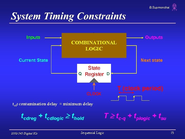
B. Supmonchai System Timing Constraints Inputs COMBINATIONAL LOGIC Current State Outputs Next state Q State Register D T (clock period) CLOCK tcd: contamination delay = minimum delay tcdreg + tcdlogic thold 2102 -545 Digital ICs T tc-q + tplogic + tsu Sequential Logic 15
B. Supmonchai Notes on System Timing Constraints q q It is important to minimize the values of the timing parameters associated with the register. In modern high-performance systems, the register propagation delay and set-up times account for a significant portion of the clock period. § DEC Alpha EV 6 has a maximum logic depth of 12 gates and the register overhead accounts for about 15% of the clock period. q Hold time becomes an issue when there is little logic between registers or when the clocks at different registers are somewhat out of phase due to clock skew. 2102 -545 Digital ICs Sequential Logic 16
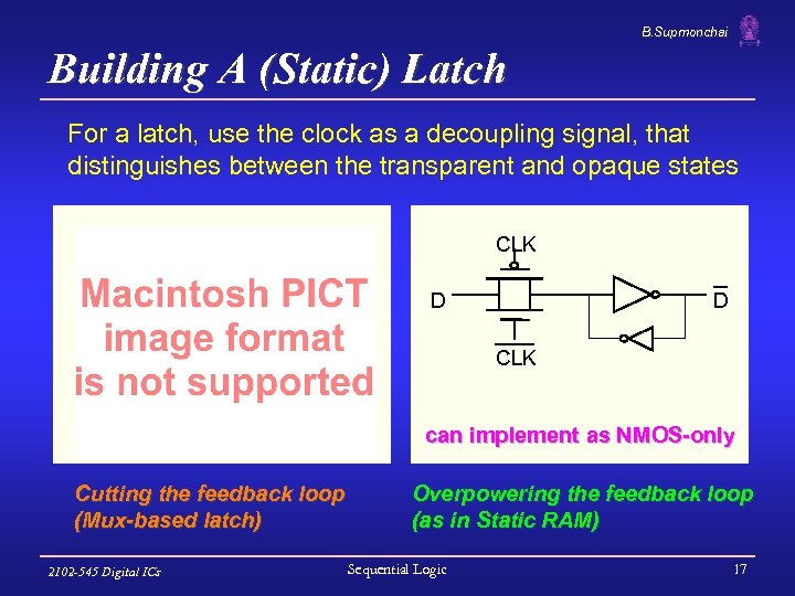
B. Supmonchai Building A (Static) Latch For a latch, use the clock as a decoupling signal, that distinguishes between the transparent and opaque states CLK D D CLK can implement as NMOS-only Cutting the feedback loop (Mux-based latch) 2102 -545 Digital ICs Overpowering the feedback loop (as in Static RAM) Sequential Logic 17
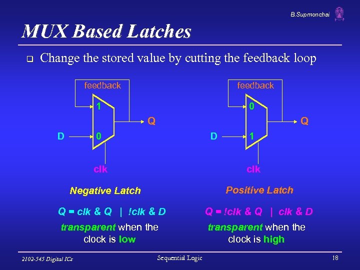
B. Supmonchai MUX Based Latches q Change the stored value by cutting the feedback loop feedback 1 0 Q D Q 0 D clk 1 clk Positive Latch Negative Latch Q = clk & Q | !clk & D Q = !clk & Q | clk & D transparent when the clock is low transparent when the clock is high 2102 -545 Digital ICs Sequential Logic 18
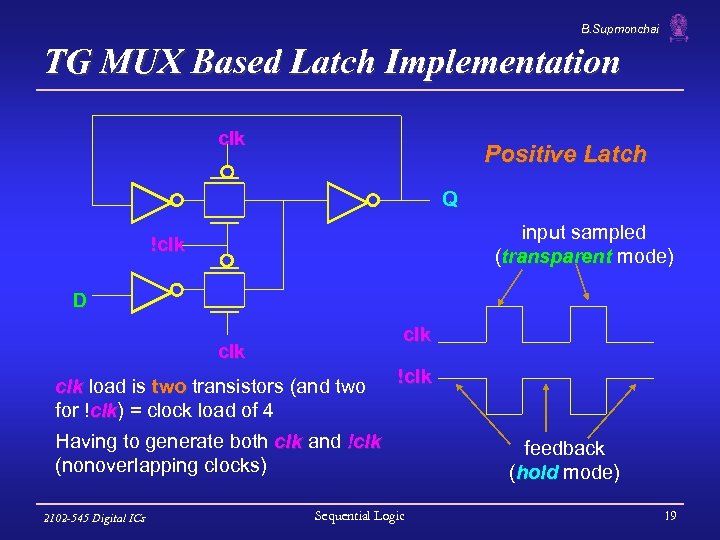
B. Supmonchai TG MUX Based Latch Implementation clk Positive Latch Q input sampled (transparent mode) !clk D clk clk load is two transistors (and two for !clk) = clock load of 4 clk !clk Having to generate both clk and !clk (nonoverlapping clocks) 2102 -545 Digital ICs Sequential Logic feedback (hold mode) 19
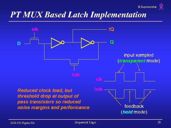
B. Supmonchai PT MUX Based Latch Implementation clk !Q Q D input sampled (transparent mode) !clk Reduced clock load, but threshold drop at output of pass transistors so reduced noise margins and performance 2102 -545 Digital ICs clk !clk Sequential Logic feedback (hold mode) 20
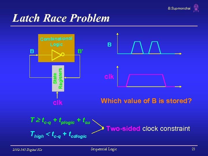
B. Supmonchai Latch Race Problem Combinational Logic B’ State Registers B clk T tc-q + tplogic + tsu Thigh tc-q + tcdlogic 2102 -545 Digital ICs B clk Which value of B is stored? Two-sided clock constraint Sequential Logic 21
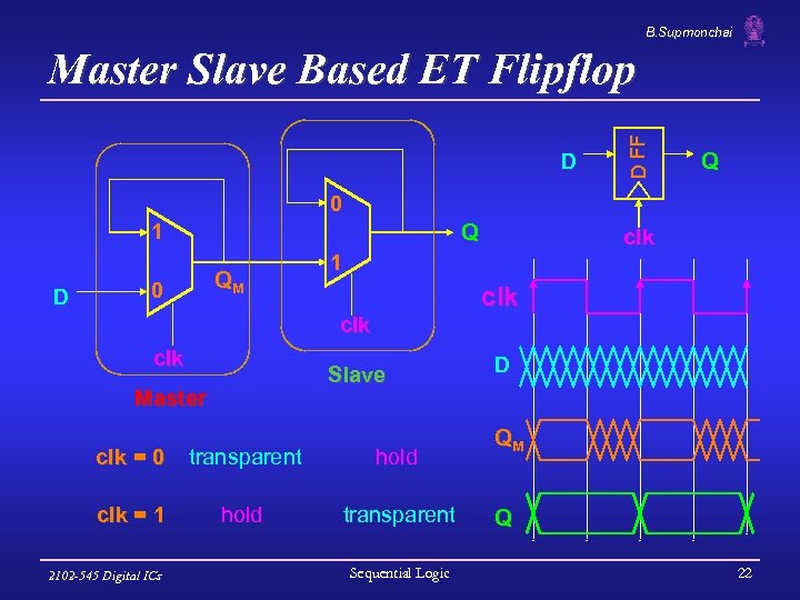
B. Supmonchai D D FF Master Slave Based ET Flipflop Q 0 1 D Q QM 0 1 clk clk Slave Master clk = 0 transparent hold clk = 1 hold transparent 2102 -545 Digital ICs clk Sequential Logic D QM Q 22
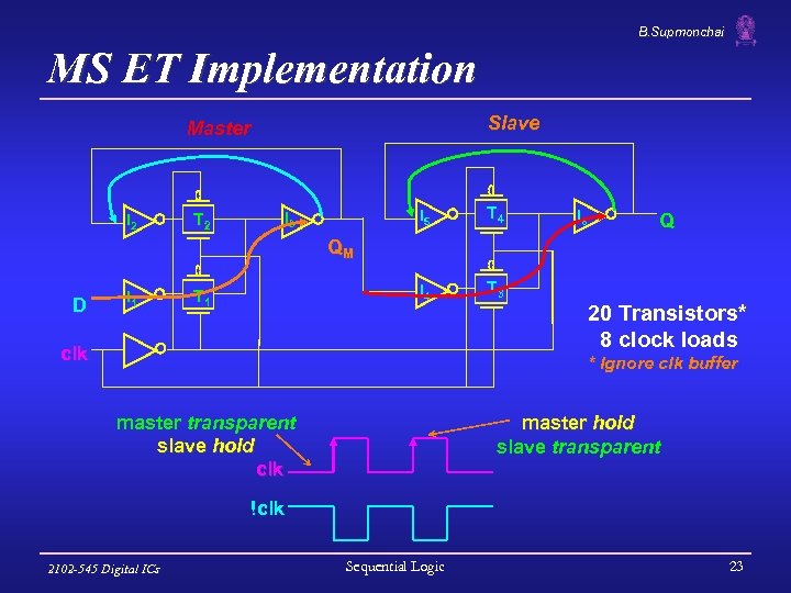
B. Supmonchai MS ET Implementation Slave Master I 2 T 2 I 5 T 4 I 3 T 3 I 6 Q QM D I 1 T 1 clk 20 Transistors* 8 clock loads * Ignore clk buffer master transparent slave hold clk master hold slave transparent !clk 2102 -545 Digital ICs Sequential Logic 23
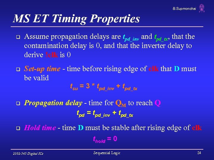
B. Supmonchai MS ET Timing Properties q q Assume propagation delays are tpd_inv and tpd_tx, that the contamination delay is 0, and that the inverter delay to derive !clk is 0 Set-up time - time before rising edge of clk that D must be valid tsu = 3 * tpd_inv + tpd_tx q Propagation delay - time for QM to reach Q tpd = tpd_inv + tpd_tx q Hold time - time D must be stable after rising edge of clk thold = 0 2102 -545 Digital ICs Sequential Logic 24
B. Supmonchai Notes on MS ET Timing Properties q Set-up time § How long before the rising edge does D have to be stable such that QM samples the value reliably? § D has to propagate through I 1, T 1, I 3 and I 2 before the rising edge to ensure that the node voltages on both terminals of T 2 are the same value. q Propagation delay time § Since the delay of I 2 is included in the set-up time, the output of I 4 is valid before the rising edge of clk, so the delay is simply the delay through T 3 and I 6 q Hold time § since T 1 turns off when the clock goes high, any changes in D after clk goes high are not seen, so hold time is 0 2102 -545 Digital ICs Sequential Logic 25
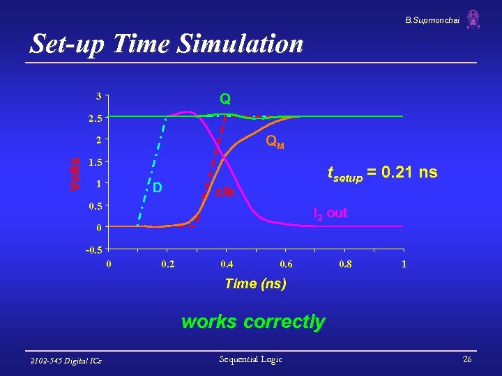
B. Supmonchai Set-up Time Simulation 3 Q 2. 5 QM Volts 2 1. 5 1 D tsetup = 0. 21 ns clk 0. 5 I 2 out 0 -0. 5 0 0. 2 0. 4 0. 6 0. 8 1 Time (ns) works correctly 2102 -545 Digital ICs Sequential Logic 26
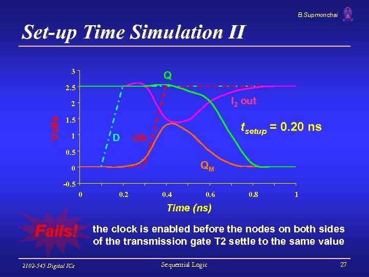
B. Supmonchai Set-up Time Simulation II 3 Q 2. 5 I 2 out Volts 2 1. 5 1 D tsetup = 0. 20 ns clk 0. 5 QM 0 -0. 5 0 0. 2 0. 4 0. 6 0. 8 1 Time (ns) Fails! 2102 -545 Digital ICs the clock is enabled before the nodes on both sides of the transmission gate T 2 settle to the same value Sequential Logic 27
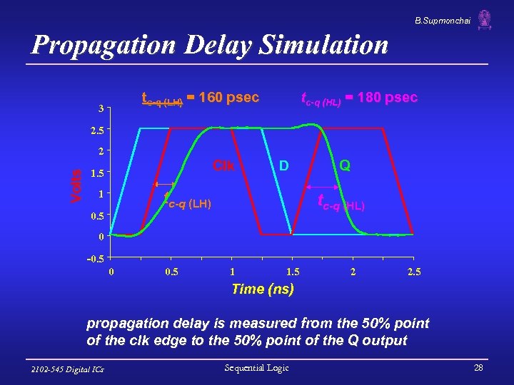
B. Supmonchai Propagation Delay Simulation tc-q (LH) = 160 psec 3 tc-q (HL) = 180 psec 2. 5 Volts 2 Clk 1. 5 D tc-q (LH) 1 0. 5 Q tc-q (HL) 0 -0. 5 0 0. 5 1 1. 5 2 2. 5 Time (ns) propagation delay is measured from the 50% point of the clk edge to the 50% point of the Q output 2102 -545 Digital ICs Sequential Logic 28
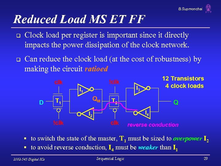
B. Supmonchai Reduced Load MS ET FF q q Clock load per register is important since it directly impacts the power dissipation of the clock network. Can reduce the clock load (at the cost of robustness) by making the circuit ratioed !clk I 1 D T 1 QM I 3 T 2 Q I 4 I 2 !clk 12 Transistors 4 clock loads clk reverse conduction § to switch the state of the master, T 1 must be sized to overpower I 2 § to avoid reverse conduction, I 4 must be weaker than I 1 2102 -545 Digital ICs Sequential Logic 29
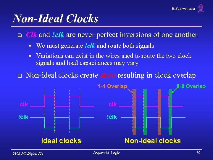
B. Supmonchai Non-Ideal Clocks q Clk and !clk are never perfect inversions of one another § We must generate !clk and route both signals § Variations can exist in the wires used to route the two clock signals and load capacitances may vary q Non-ideal clocks create skew resulting in clock overlap 1 -1 Overlap clk !clk 0 -0 Overlap !clk Ideal clocks 2102 -545 Digital ICs Non-Ideal clocks Sequential Logic 30
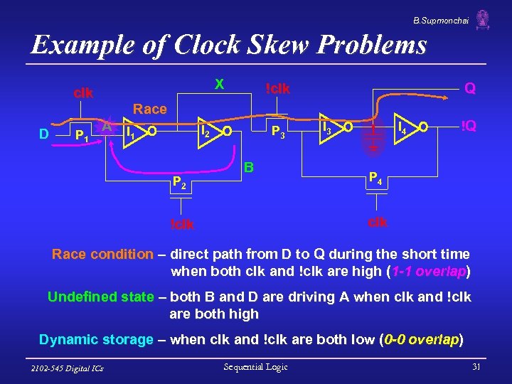
B. Supmonchai Example of Clock Skew Problems X clk D P 1 Q !clk Race A I 1 I 2 P 3 B I 3 I 4 !Q P 4 clk !clk Race condition – direct path from D to Q during the short time when both clk and !clk are high (1 -1 overlap) Undefined state – both B and D are driving A when clk and !clk are both high Dynamic storage – when clk and !clk are both low (0 -0 overlap) 2102 -545 Digital ICs Sequential Logic 31
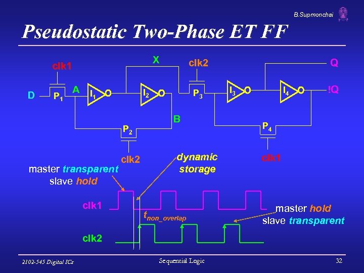
B. Supmonchai Pseudostatic Two-Phase ET FF X clk 1 D P 1 A I 1 I 2 P 2 master transparent slave hold clk 1 clk 2 Q clk 2 P 3 B dynamic storage tnon_overlap I 3 I 4 !Q P 4 clk 1 master hold slave transparent clk 2 2102 -545 Digital ICs Sequential Logic 32
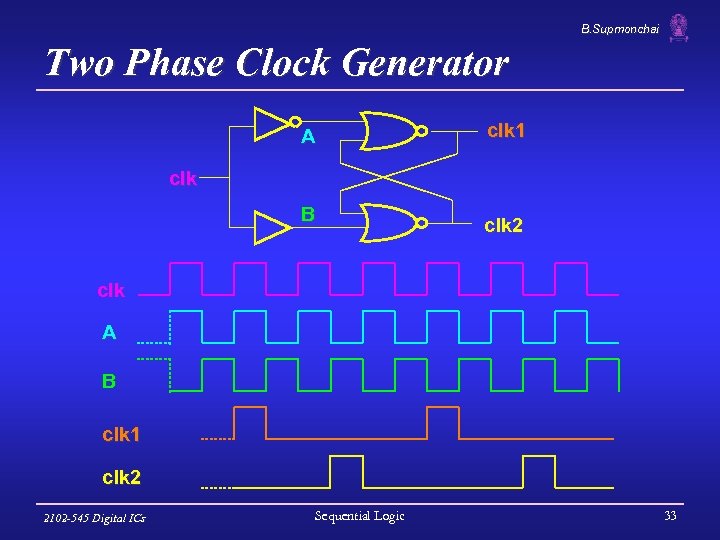
B. Supmonchai Two Phase Clock Generator A clk 1 clk B clk 2 clk A B clk 1 clk 2 2102 -545 Digital ICs Sequential Logic 33
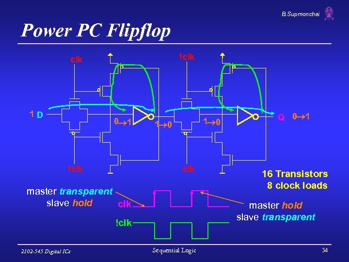
B. Supmonchai Power PC Flipflop !clk 1 D 0 1 !clk 1 0 clk master transparent slave hold clk 16 Transistors 8 clock loads master hold slave transparent !clk 2102 -545 Digital ICs Q 0 1 Sequential Logic 34
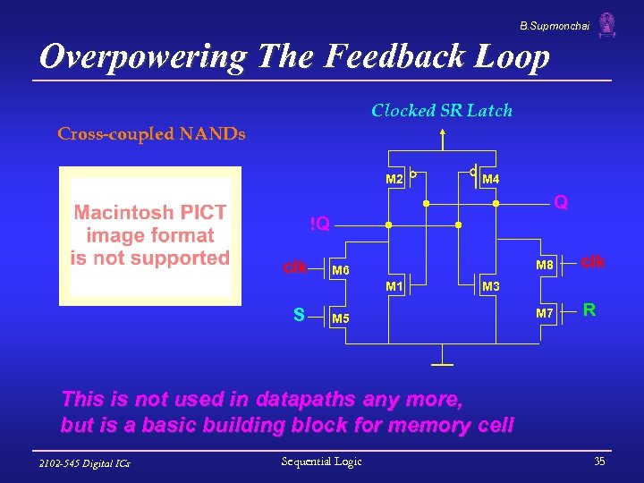
B. Supmonchai Overpowering The Feedback Loop Clocked SR Latch Cross-coupled NANDs M 2 M 4 Q !Q clk M 8 M 6 M 1 S clk M 7 R M 3 M 5 This is not used in datapaths any more, but is a basic building block for memory cell 2102 -545 Digital ICs Sequential Logic 35
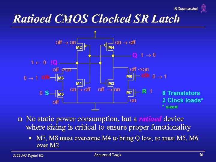
B. Supmonchai Ratioed CMOS Clocked SR Latch off on M 2 M 4 on off Q 1 0 1 0 !Q off ->on 0 1 clk off ->on M 8 M 6 M 1 0 S M 5 on off M 7 R 1 M 3 off on on off q clk 0 1 8 Transistors 2 Clock loads* * sized No static power consumption, but a ratioed device where sizing is critical to ensure proper functionality § M 7, M 8 must overcome M 4 to bring Q low, so must M 5, M 6 over M 2 2102 -545 Digital ICs Sequential Logic 36
B. Supmonchai Sizing Issues !Q (Volts) (W/L)2 and 4 = 1. 5 m/0. 25 m (W/L)1 and 3 = 0. 5 m/0. 25 m so (W/L)5 and 6 > 3 (W/L)5 and 6 Output voltage depends on pull-down transistor width 2102 -545 Digital ICs Sequential Logic 37
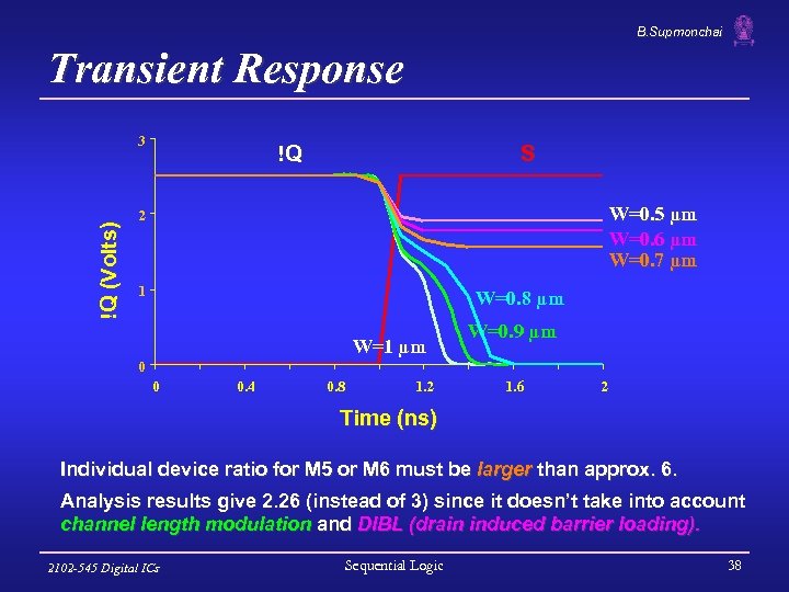
B. Supmonchai Transient Response !Q (Volts) 3 !Q S W=0. 5 µm W=0. 6 µm W=0. 7 µm 2 1 W=0. 8 µm W=1 µm W=0. 9 µm 0 0 0. 4 0. 8 1. 2 1. 6 2 Time (ns) Individual device ratio for M 5 or M 6 must be larger than approx. 6. Analysis results give 2. 26 (instead of 3) since it doesn’t take into account channel length modulation and DIBL (drain induced barrier loading). 2102 -545 Digital ICs Sequential Logic 38
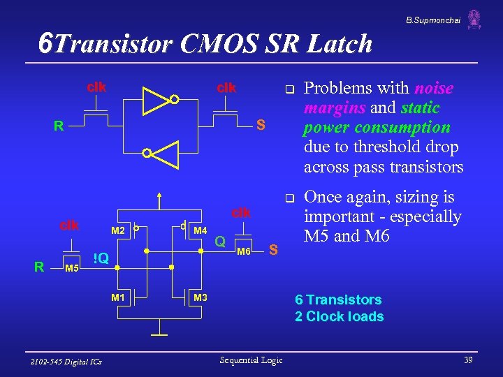
B. Supmonchai 6 Transistor CMOS SR Latch clk q S R clk R M 5 q M 2 M 4 !Q M 1 2102 -545 Digital ICs Q M 6 S Problems with noise margins and static power consumption due to threshold drop across pass transistors Once again, sizing is important - especially M 5 and M 6 6 Transistors 2 Clock loads M 3 Sequential Logic 39
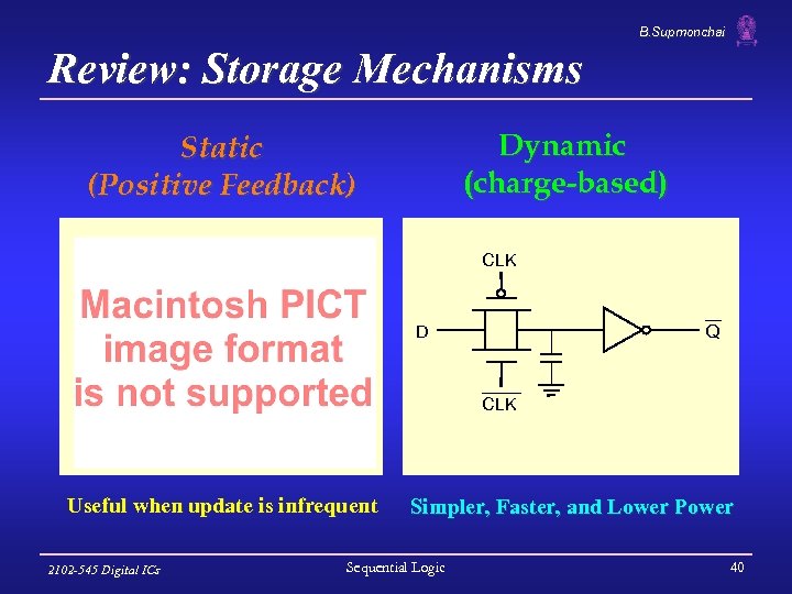
B. Supmonchai Review: Storage Mechanisms Dynamic (charge-based) Static (Positive Feedback) CLK D Q CLK Useful when update is infrequent 2102 -545 Digital ICs Simpler, Faster, and Lower Power Sequential Logic 40
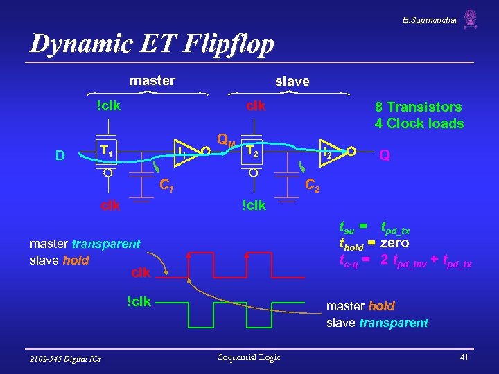
B. Supmonchai Dynamic ET Flipflop master slave !clk D clk T 1 I 1 QM T 2 C 1 clk I 2 Q C 2 !clk tsu = tpd_tx thold = zero tc-q = 2 tpd_inv + tpd_tx master transparent slave hold clk !clk 2102 -545 Digital ICs 8 Transistors 4 Clock loads master hold slave transparent Sequential Logic 41
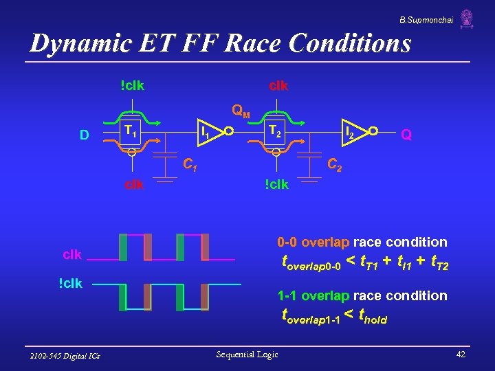
B. Supmonchai Dynamic ET FF Race Conditions !clk QM D T 1 I 1 T 2 C 1 clk !clk I 2 Q C 2 !clk 0 -0 overlap race condition toverlap 0 -0 < t. T 1 + t. I 1 + t. T 2 1 -1 overlap race condition toverlap 1 -1 < thold 2102 -545 Digital ICs Sequential Logic 42
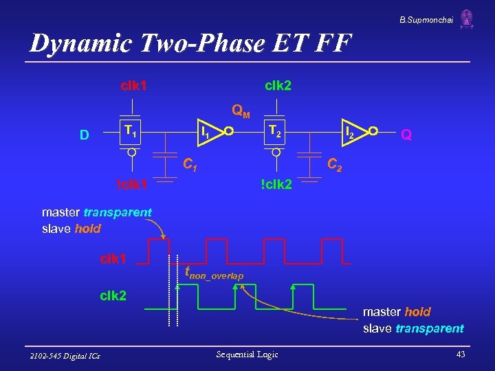
B. Supmonchai Dynamic Two-Phase ET FF clk 1 clk 2 QM T 1 D T 2 I 1 C 1 I 2 Q C 2 !clk 1 !clk 2 master transparent slave hold clk 1 tnon_overlap clk 2 master hold slave transparent 2102 -545 Digital ICs Sequential Logic 43
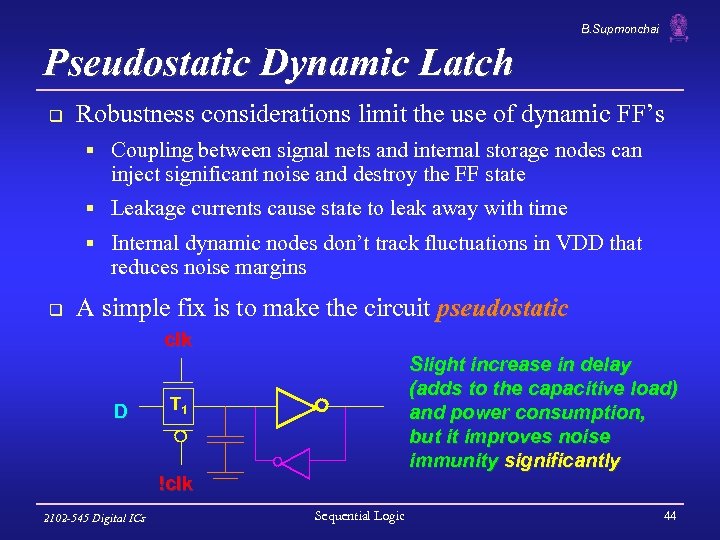
B. Supmonchai Pseudostatic Dynamic Latch q Robustness considerations limit the use of dynamic FF’s § Coupling between signal nets and internal storage nodes can inject significant noise and destroy the FF state § Leakage currents cause state to leak away with time § Internal dynamic nodes don’t track fluctuations in VDD that reduces noise margins q A simple fix is to make the circuit pseudostatic clk D Slight increase in delay (adds to the capacitive load) and power consumption, but it improves noise immunity significantly T 1 !clk 2102 -545 Digital ICs Sequential Logic 44
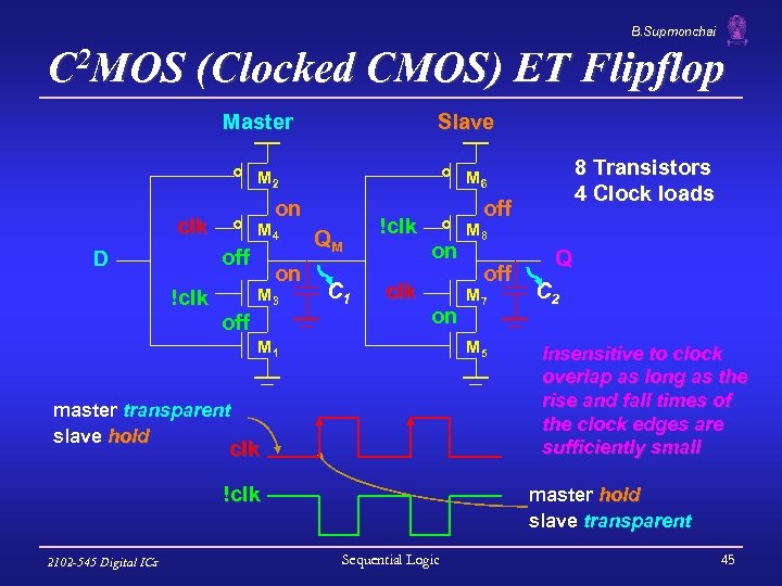
B. Supmonchai C 2 MOS (Clocked CMOS) ET Flipflop Master Slave M 2 on clk M 4 off D !clk on M 3 off QM C 1 !clk off on on M 1 M 8 off M 7 M 5 master transparent slave hold clk !clk 2102 -545 Digital ICs 8 Transistors 4 Clock loads M 6 Q C 2 Insensitive to clock overlap as long as the rise and fall times of the clock edges are sufficiently small master hold slave transparent Sequential Logic 45
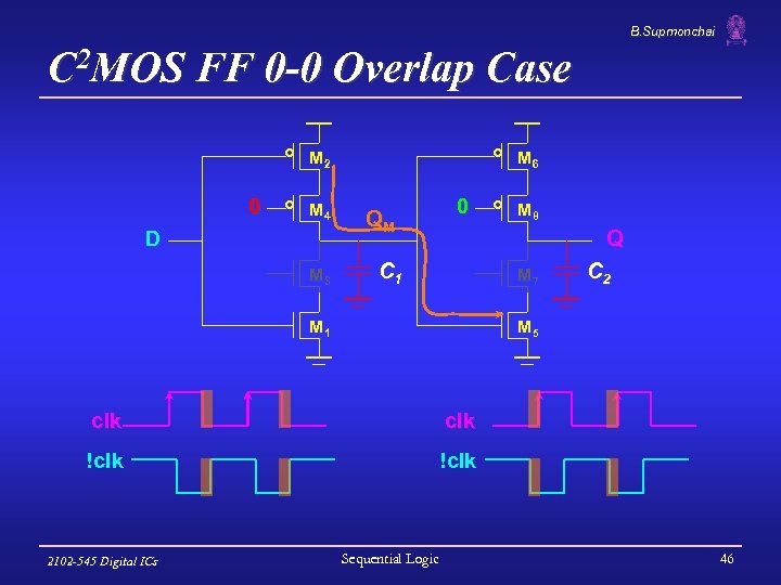
B. Supmonchai C 2 MOS FF 0 -0 Overlap Case M 2 0 M 4 D M 3 M 6 QM 0 M 8 Q C 1 M 7 M 1 C 2 M 5 clk !clk 2102 -545 Digital ICs Sequential Logic 46
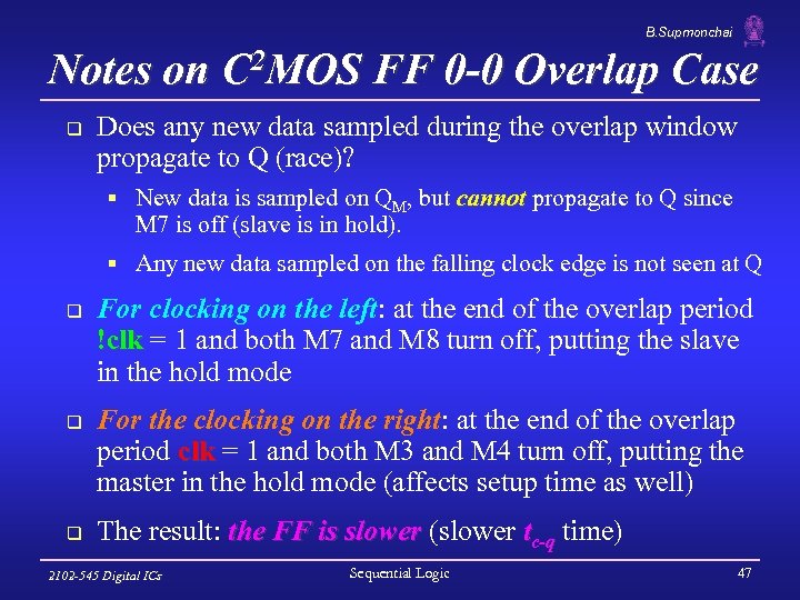
B. Supmonchai Notes on C 2 MOS FF 0 -0 Overlap Case q Does any new data sampled during the overlap window propagate to Q (race)? § New data is sampled on QM, but cannot propagate to Q since M 7 is off (slave is in hold). § Any new data sampled on the falling clock edge is not seen at Q q q q For clocking on the left: at the end of the overlap period !clk = 1 and both M 7 and M 8 turn off, putting the slave in the hold mode For the clocking on the right: at the end of the overlap period clk = 1 and both M 3 and M 4 turn off, putting the master in the hold mode (affects setup time as well) The result: the FF is slower (slower tc-q time) 2102 -545 Digital ICs Sequential Logic 47
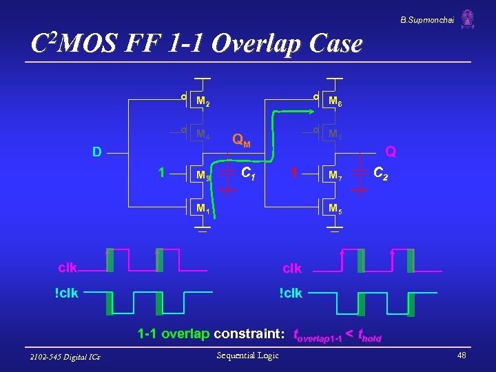
B. Supmonchai C 2 MOS FF 1 -1 Overlap Case M 2 M 4 D 1 M 3 M 6 M 8 QM C 1 Q 1 M 7 C 2 M 5 clk !clk 1 -1 overlap constraint: toverlap 1 -1 < thold 2102 -545 Digital ICs Sequential Logic 48
B. Supmonchai Notes on C 2 MOS FF 1 -1 Overlap Case q q New data is sampled on QM, but cannot propagate to Q since M 8 is off (slave is in hold). A bit more problematic than 0 -0 overlap. § It must enforce a hold time on D, so that changing D which reaches QM is not copied to Q when overlap time is over - Ø first clocking condition. § By imposing a hold time on D - that D must be stable during clock overlap - overcome this problem as well q However, possible race can occur if the rise/fall times of the clock are sufficiently slow. § Works correctly as long as the clock rise/fall times is smaller than approximately five times the propagation delay of the flipflop. 2102 -545 Digital ICs Sequential Logic 49
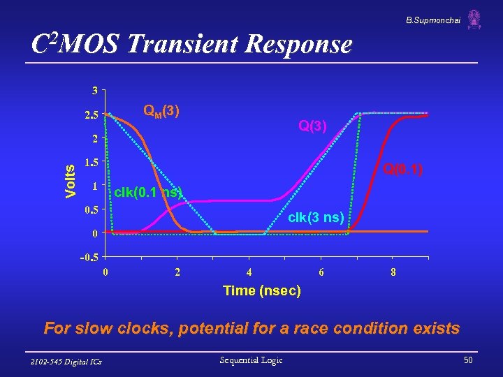
B. Supmonchai C 2 MOS Transient Response 3 QM(3) 2. 5 Q(3) Volts 2 1. 5 Q(0. 1) 1 clk(0. 1 ns) 0. 5 clk(3 ns) 0 -0. 5 0 2 4 6 8 Time (nsec) For slow clocks, potential for a race condition exists 2102 -545 Digital ICs Sequential Logic 50
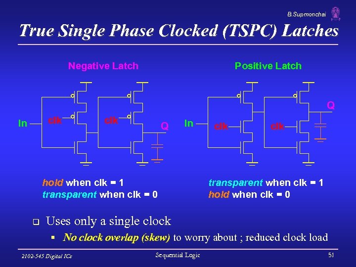
B. Supmonchai True Single Phase Clocked (TSPC) Latches Negative Latch Positive Latch Q clk In clk Q In hold when clk = 1 transparent when clk = 0 q clk transparent when clk = 1 hold when clk = 0 Uses only a single clock § No clock overlap (skew) to worry about ; reduced clock load 2102 -545 Digital ICs Sequential Logic 51
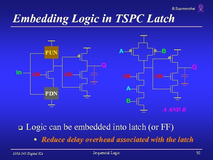
B. Supmonchai Embedding Logic in TSPC Latch A PUN B Q In clk Q clk A PDN B A AND B q Logic can be embedded into latch (or FF) § Reduce delay overhead associated with the latch 2102 -545 Digital ICs Sequential Logic 52
B. Supmonchai Notes on Embedding Logic in TSPC Latch q Set-up time increased, but overall performance increased improved § The increase in the set-up time is typically smaller than the delay of an AND gate. § For example, using minimum size devices set-up of AND latch is 140 psec. § Using the conventional approach of AND gate followed by latch has an effective set-up time of 600 psec. q Technique used extensively in the design of the EV 4 DEC Alpha microprocessor and many other high performance processors. 2102 -545 Digital ICs Sequential Logic 53
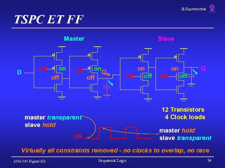
B. Supmonchai TSPC ET FF Master D clk on off clk Slave on QM off on clk Q off 12 Transistors 4 Clock loads master transparent slave hold master hold slave transparent clk Virtually all constraints removed - no clocks to overlap, no race 2102 -545 Digital ICs Sequential Logic 54
B. Supmonchai Notes on TSPC ET FF q Warning! - similar to C 2 MOS, TSPC flipflops malfunction when the slope of the clock is not sufficiently steep § Slow clock cause both the NMOS and PMOS clocked transistors to be ON simultaneously, resulting in undefined values of the states and race conditions. § Clock slopes thus must be carefully engineered. If necessary, local buffers must be introduced to ensure the quality of the clock signal 2102 -545 Digital ICs Sequential Logic 55
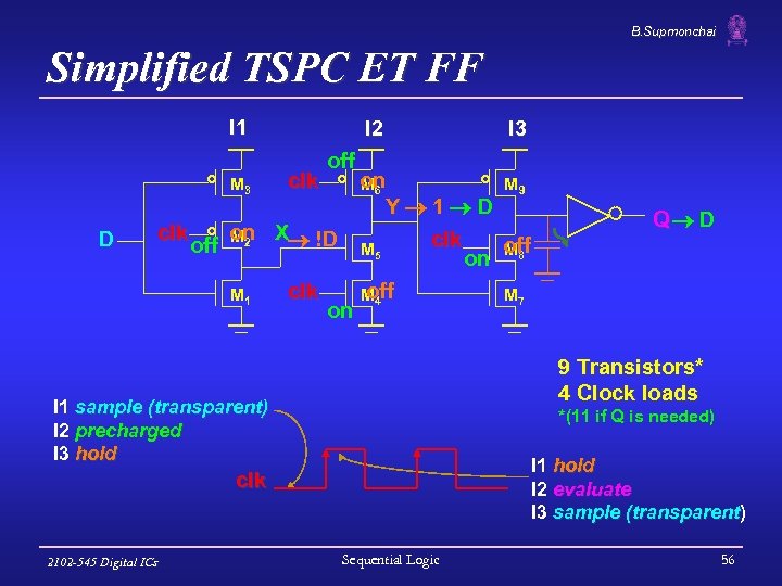
B. Supmonchai Simplified TSPC ET FF I 1 clk I 3 off on M 6 M 9 Y 1 D on X !D clk off M 2 off M 5 on M 8 clk off M 1 M 4 M 7 on M 3 D I 2 9 Transistors* 4 Clock loads I 1 sample (transparent) I 2 precharged I 3 hold *(11 if Q is needed) I 1 hold I 2 evaluate I 3 sample (transparent) (transparent clk 2102 -545 Digital ICs Q D Sequential Logic 56
B. Supmonchai Notes on TSPC ET FF q On the positive edge of the clock, note that the node X transitions to a low if D is high. Therefore, the input must be kept stable until the value on node X before the rising edge of the clock propagates to Y § Hold time of the register (less than 1 inverter delay since it takes 1 inverter delay for the input to affect node X). q q Propagation delay is essentially three inverters since the value on node X must propagate to output Q Set-up time is the time for node X to be valid – one inverter delay 2102 -545 Digital ICs Sequential Logic 57
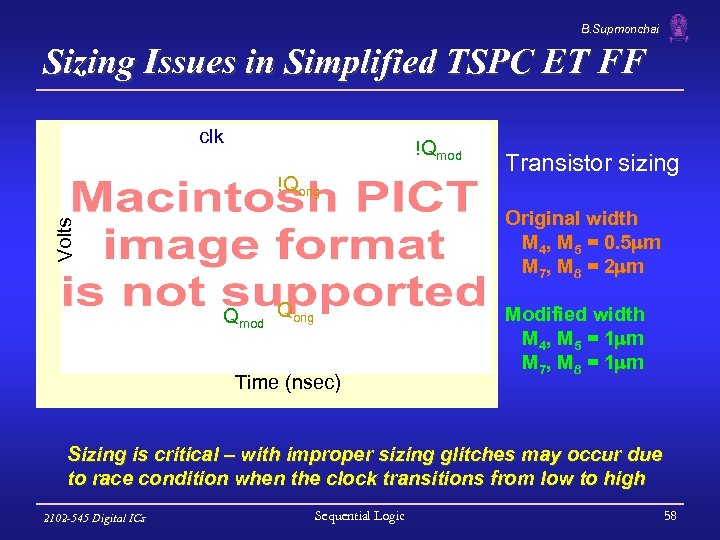
B. Supmonchai Sizing Issues in Simplified TSPC ET FF clk !Qmod !Qorig Transistor sizing Volts Original width M 4, M 5 = 0. 5 m M 7 , M 8 = 2 m Qmod Qorig Time (nsec) Modified width M 4 , M 5 = 1 m M 7 , M 8 = 1 m Sizing is critical – with improper sizing glitches may occur due to race condition when the clock transitions from low to high 2102 -545 Digital ICs Sequential Logic 58
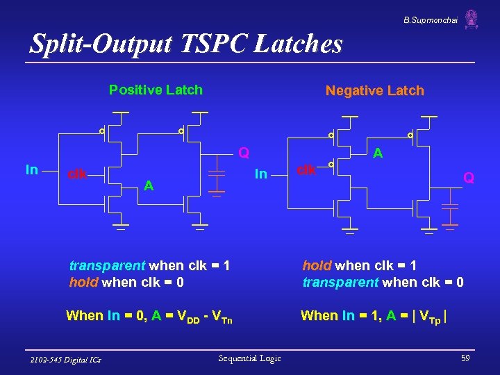
B. Supmonchai Split-Output TSPC Latches Positive Latch Negative Latch Q In clk A In A clk Q transparent when clk = 1 hold when clk = 0 hold when clk = 1 transparent when clk = 0 When In = 0, A = VDD - VTn When In = 1, A = | VTp | 2102 -545 Digital ICs Sequential Logic 59
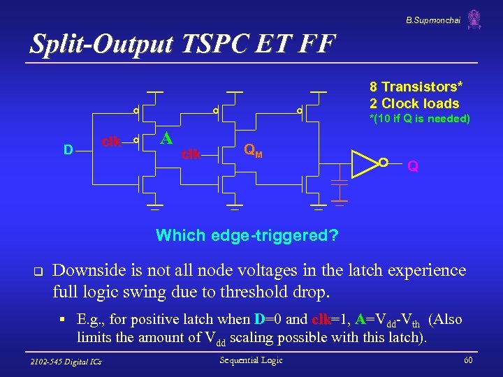
B. Supmonchai Split-Output TSPC ET FF 8 Transistors* 2 Clock loads *(10 if Q is needed) D clk A clk QM Q Which edge-triggered? q Downside is not all node voltages in the latch experience full logic swing due to threshold drop. § E. g. , for positive latch when D=0 and clk=1, A=Vdd-Vth (Also clk limits the amount of Vdd scaling possible with this latch). 2102 -545 Digital ICs Sequential Logic 60
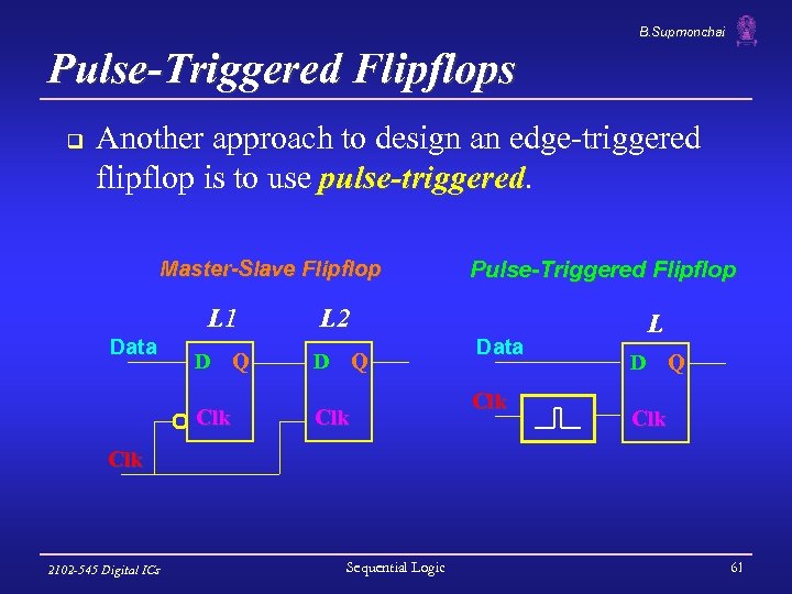
B. Supmonchai Pulse-Triggered Flipflops q Another approach to design an edge-triggered flipflop is to use pulse-triggered Master-Slave Flipflop L 1 Data D Clk Q Pulse-Triggered Flipflop L 2 D Q Clk Data Clk L D Q Clk 2102 -545 Digital ICs Sequential Logic 61
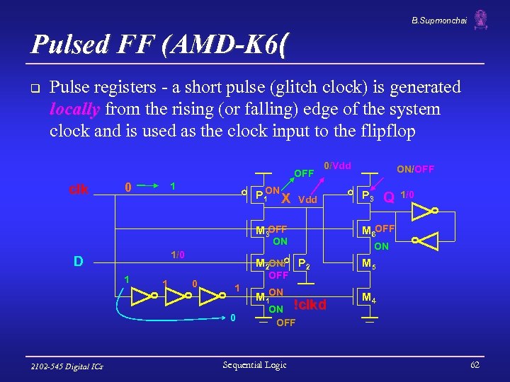
B. Supmonchai Pulsed FF (AMD-K 6( q Pulse registers - a short pulse (glitch clock) is generated locally from the rising (or falling) edge of the system clock and is used as the clock input to the flipflop OFF clk 0 1 0/Vdd ON/OFF ON P 1 X Vdd P 3 M 3 OFF M 6 OFF ON 1/0 D 1 1 0 2102 -545 Digital ICs P 2 OFF 1 M 1 ON !clkd ON OFF Sequential Logic 1/0 ON M 2 ON/ 0 Q M 5 M 4 62
B. Supmonchai Notes on Pulsed FF q q q Race conditions are avoided by keeping the transparent mode time very short (during the pulse only) Reduce clock load but substantially increase complexity in verification The transparency period determines the hold time. § The window must be wide enough for the input data to propagate to Q. q The set-up time can be NEGATIVE (if the transparency window is longer than the delay from input to output). § This is attractive, as data can arrive at the register even after the clock goes high, meaning that time can be borrowed from the previous cycle. 2102 -545 Digital ICs Sequential Logic 63
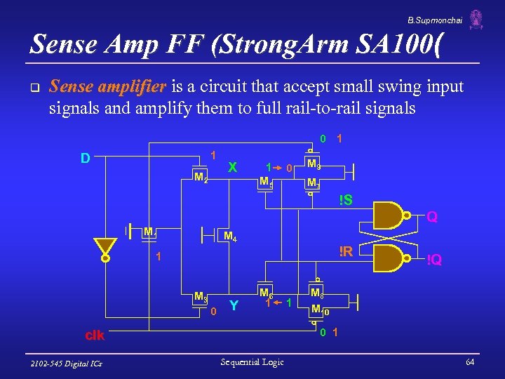
B. Supmonchai Sense Amp FF (Strong. Arm SA 100( q Sense amplifier is a circuit that accept small swing input signals and amplify them to full rail-to-rail signals 0 1 1 D M 2 X 1 M 5 0 M 9 M 7 !S Q M 1 M 4 !R 1 M 3 0 Y M 6 1 M 8 M 10 0 1 clk 2102 -545 Digital ICs 1 !Q Sequential Logic 64
B. Supmonchai Notes on Sensed Amp FF q The key is transistor M 4 (in the middle of Sensed amp); it delays signals that pass through to the other side of its terminal, making the change on the other side slower § When D = 1, Y changes after X due to the delay of M 4. By the time M 6 reacts to the change at its terminal, it is already turned off by the terminal voltage at M 4 (a 0). Thus, M 6 holds a 1. q q M 4 also provides DC-leakage path to ground for either node X or Y in case that the inputs change their value after the positive edge of CLK arrives. Advantages are reduced clock load and that it can be used as a receiver for reduced swing differential buses § Where does the differential signal enter? 2102 -545 Digital ICs Sequential Logic 65
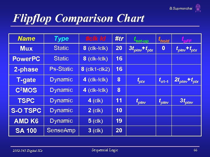
B. Supmonchai Flipflop Comparison Chart Name Mux Type #clk ld #tr tset-up thold tp. FF Static 8 (clk-!clk) 20 3 tpinv+tptx 0 tpinv+tptx Power. PC Static 8 (clk-!clk) 16 2 -phase Ps-Static 8 (clk 1 -clk 2) 16 T-gate Dynamic 4 (clk-!clk) 8 C 2 MOS Dynamic 4 (clk-!clk) 8 TSPC Dynamic 4 (clk) 11 S-O TSPC Dynamic 2 (clk) 10 AMD K 6 Dynamic 5 (clk) 19 SA 100 Sense. Amp 3 (clk) 20 2102 -545 Digital ICs Sequential Logic tptx to 1 -1 2 tpinv+tptx tpinv 3 tpinv 66
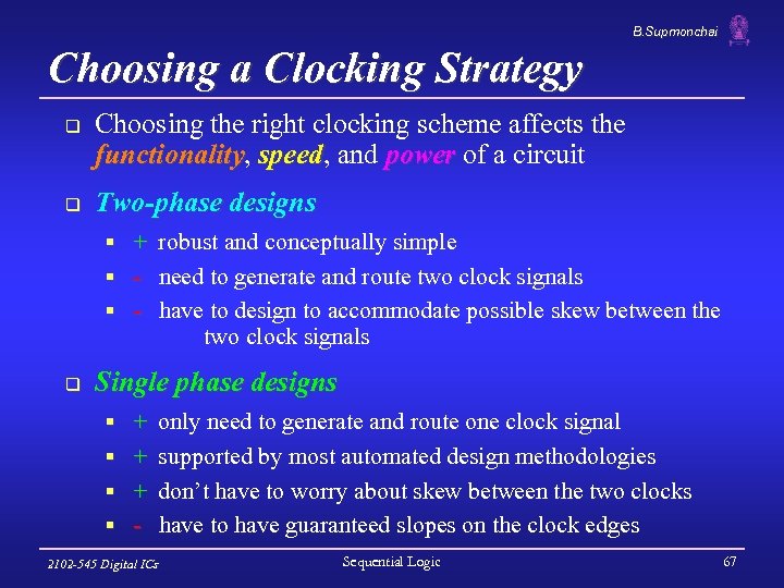
B. Supmonchai Choosing a Clocking Strategy q q Choosing the right clocking scheme affects the functionality, speed, and power of a circuit functionality speed Two-phase designs § + robust and conceptually simple § - need to generate and route two clock signals § - have to design to accommodate possible skew between the two clock signals q Single phase designs § + only need to generate and route one clock signal § + supported by most automated design methodologies § + don’t have to worry about skew between the two clocks § - have to have guaranteed slopes on the clock edges 2102 -545 Digital ICs Sequential Logic 67
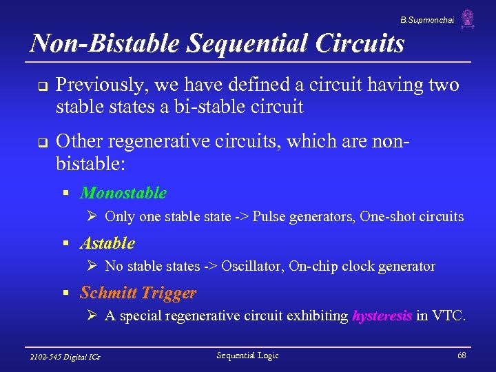
B. Supmonchai Non-Bistable Sequential Circuits q q Previously, we have defined a circuit having two stable states a bi-stable circuit Other regenerative circuits, which are nonbistable: § Monostable Ø Only one stable state -> Pulse generators, One-shot circuits § Astable Ø No stable states -> Oscillator, On-chip clock generator § Schmitt Trigger Ø A special regenerative circuit exhibiting hysteresis in VTC. 2102 -545 Digital ICs Sequential Logic 68
B. Supmonchai Schmitt Trigger Non-Bistable Sequential Circuits 2 important properties § Hysteresis § Fast Transition Time at the output 2102 -545 Digital ICs Sequential Logic 69
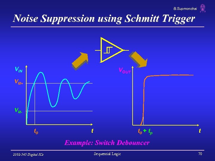
B. Supmonchai Noise Suppression using Schmitt Trigger VIN VOUT VM+ VM- t 0 t t 0 + tp t Example: Switch Debouncer 2102 -545 Digital ICs Sequential Logic 70
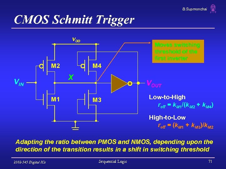
B. Supmonchai CMOS Schmitt Trigger VDD M 2 Moves switching threshold of the first inverter M 4 X VIN M 1 VOUT M 3 Low-to-High reff = k. M 1/(k. M 2 + k. M 4) High-to-Low reff = (k. M 1 + k. M 3)/k. M 2 Adapting the ratio between PMOS and NMOS, depending upon the direction of the transition results in a shift in switching threshold 2102 -545 Digital ICs Sequential Logic 71
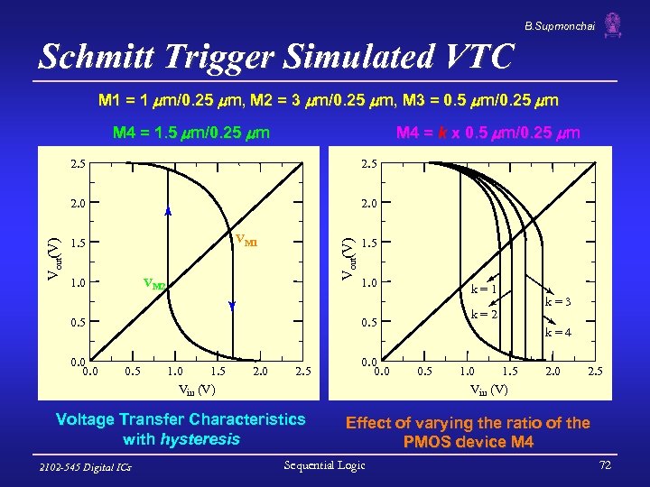
B. Supmonchai Schmitt Trigger Simulated VTC M 1 = 1 m/0. 25 m, M 2 = 3 m/0. 25 m, M 3 = 0. 5 m/0. 25 m M 4 = 1. 5 m/0. 25 m M 4 = k x 0. 5 m/0. 25 m 2. 5 2. 0 VM 1 1. 5 1. 0 Vout(V) 2. 5 VM 2 0. 5 0. 0 1. 5 1. 0 k=1 k=2 0. 5 1. 0 1. 5 Vin (V) 2. 0 2. 5 Voltage Transfer Characteristics with hysteresis 2102 -545 Digital ICs 0. 0 k=3 k=4 0. 5 1. 0 1. 5 Vin (V) 2. 0 2. 5 Effect of varying the ratio of the PMOS device M 4 Sequential Logic 72
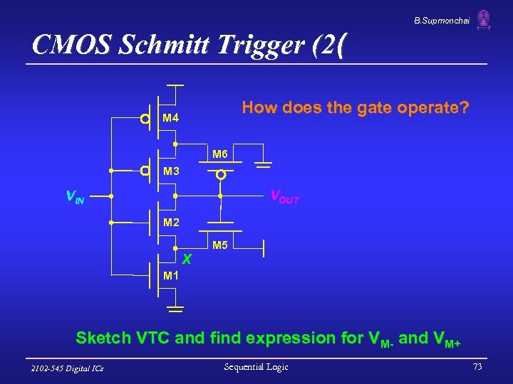
B. Supmonchai CMOS Schmitt Trigger (2( How does the gate operate? M 4 M 6 M 3 VOUT VIN M 2 X M 5 M 1 Sketch VTC and find expression for VM- and VM+ 2102 -545 Digital ICs Sequential Logic 73
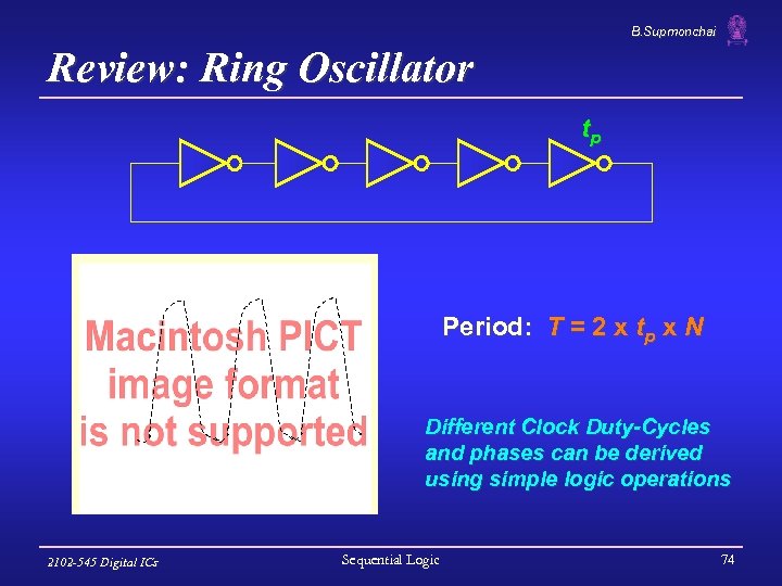
B. Supmonchai Review: Ring Oscillator tp Period: T = 2 x tp x N Different Clock Duty-Cycles and phases can be derived using simple logic operations 2102 -545 Digital ICs Sequential Logic 74
B. Supmonchai Voltage Controller Oscillator (VCO( q Oscillation frequency of a VCO is a function (typically nonlinear) of a control voltage Delay of a current starved inverter depends on the current limit available to discharge the load capacitance of the gate 2102 -545 Digital ICs Sequential Logic 75
B. Supmonchai Current-Starved Inverter Simulation tp. HL (nsec) q § Delay sensitive to Vctrl (V) 2102 -545 Digital ICs The device is in the subthreshold region when Vctrl is smaller than VT, resulting in large variations of tp as the drive current is exponentially dependent on the drive voltage noise and variation in Vctrl Sequential Logic 76
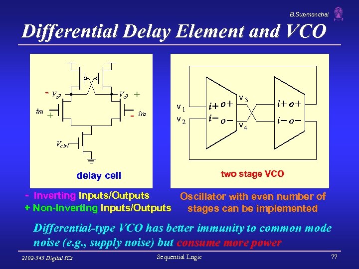
B. Supmonchai Differential Delay Element and VCO - Vo 2 in 1 Vo 1 + + - in 2 v 1 v 2 v 3 v 4 Vctrl two stage VCO delay cell - Inverting Inputs/Outputs Oscillator with even number of + Non-Inverting Inputs/Outputs stages can be implemented Differential-type VCO has better immunity to common mode noise (e. g. , supply noise) but consume more power 2102 -545 Digital ICs Sequential Logic 77
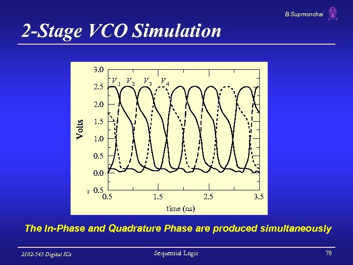
B. Supmonchai 2 -Stage VCO Simulation 3. 0 2. 5 V 1 V 2 V 3 V 4 2. 0 1. 5 1. 0 0. 5 0. 0 2 0. 5 1. 5 2. 5 3. 5 time (ns) The In-Phase and Quadrature Phase are produced simultaneously 2102 -545 Digital ICs Sequential Logic 78
d6295e938c88c1feee3957d1dc49858d.ppt