d097fb8c16f58f6b0d3fd061511db3c2.ppt
- Количество слайдов: 108
Chapter 4 Input/Output Organization
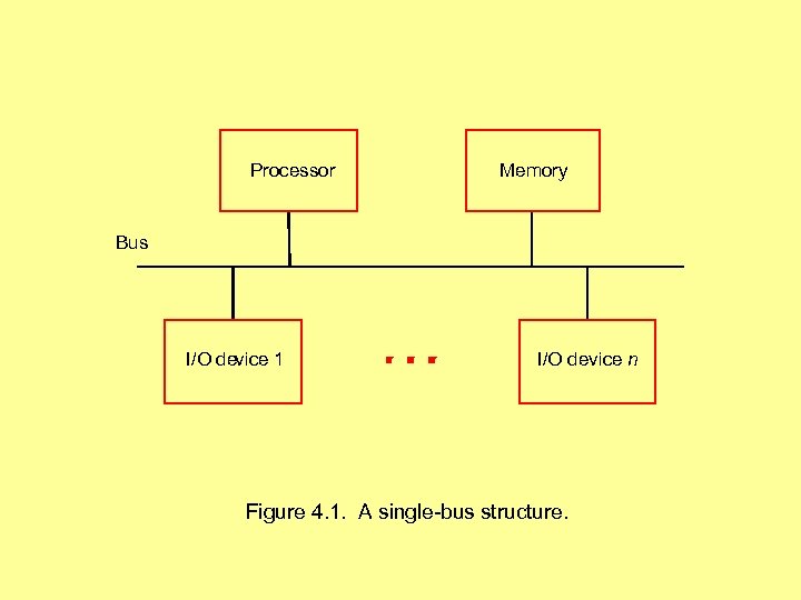
Processor Memory Bus I/O device 1 I/O device n Figure 4. 1. A single-bus structure.
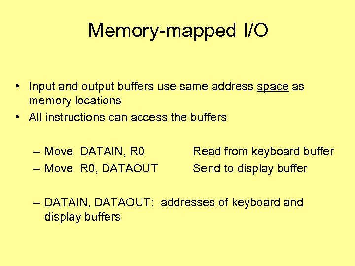
Memory-mapped I/O • Input and output buffers use same address space as memory locations • All instructions can access the buffers – Move DATAIN, R 0 – Move R 0, DATAOUT Read from keyboard buffer Send to display buffer – DATAIN, DATAOUT: addresses of keyboard and display buffers
Isolated I/O • Separate address space for I/O devices • Special instructions (e. g. , IN, OUT) that indicate that the address is not in memory address space • Intel processors can use either
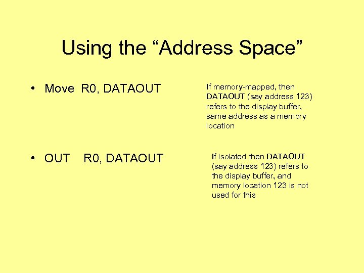
Using the “Address Space” • Move R 0, DATAOUT • OUT R 0, DATAOUT If memory-mapped, then DATAOUT (say address 123) refers to the display buffer, same address as a memory location If isolated then DATAOUT (say address 123) refers to the display buffer, and memory location 123 is not used for this
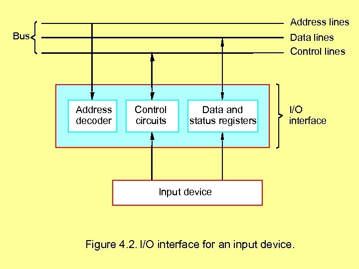
Address lines Bus Data lines Control lines Address decoder Control circuits Data and status registers I/O interface Input device Figure 4. 2. I/O interface for an input device.
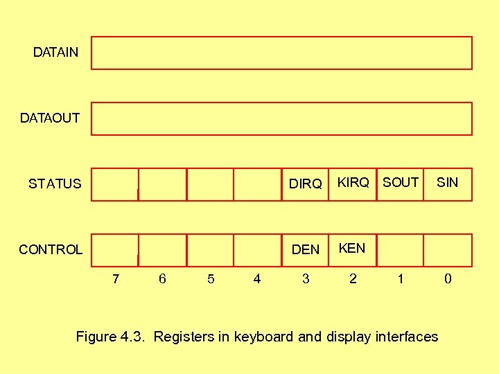
DATAIN DATAOUT STATUS DIRQ KIRQ SOUT CONTROL DEN KEN 3 2 7 6 5 4 SIN 1 Figure 4. 3. Registers in keyboard and display interfaces 0
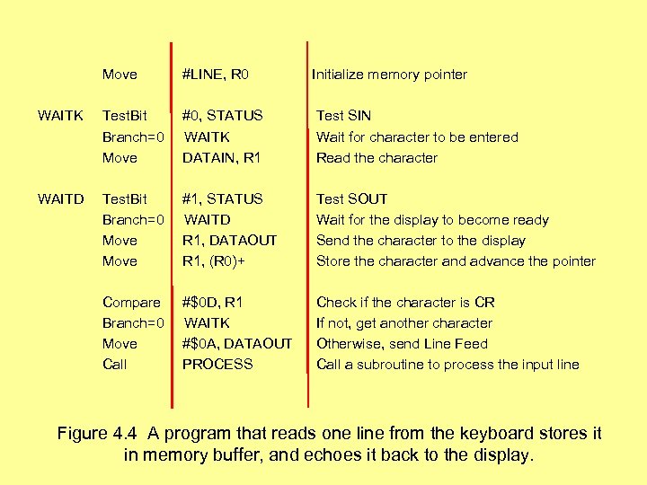
Move #LINE, R 0 Initialize memory pointer WAITK Test. Bit Branch=0 Move #0, STATUS WAITK DATAIN, R 1 Test SIN Wait for character to be entered Read the character WAITD Test. Bit Branch=0 Move #1, STATUS WAITD R 1, DATAOUT R 1, (R 0)+ Test SOUT Wait for the display to become ready Send the character to the display Store the character and advance the pointer Compare Branch=0 Move Call #$0 D, R 1 WAITK #$0 A, DATAOUT PROCESS Check if the character is CR If not, get another character Otherwise, send Line Feed Call a subroutine to process the input line Figure 4. 4 A program that reads one line from the keyboard stores it in memory buffer, and echoes it back to the display.
Interrupts • Interrupt-request line – Interrupt-request signal – Interrupt-acknowledge signal • Interrupt-service routine – Similar to subroutine – May have no relationship to program being executed at time of interrupt • Program info must be saved • Interrupt latency
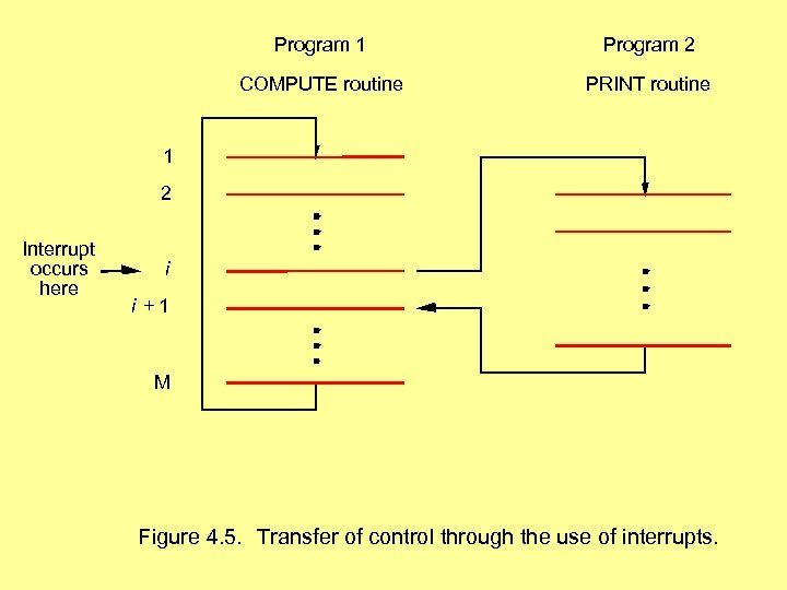
Program 1 Program 2 COMPUTE routine PRINT routine 1 2 Interrupt occurs here i i +1 M Figure 4. 5. Transfer of control through the use of interrupts.
Handling Interrupts • Many situations where the processor should ignore interrupt requests – Interrupt-disable – Interrupt-enable • Typical scenario – Device raises interrupt request – Processor interrupts program being executed – Processor disables interrupts and acknowledges interrupt – Interrupt-service routine executed – Interrupts enabled and program execution resumed
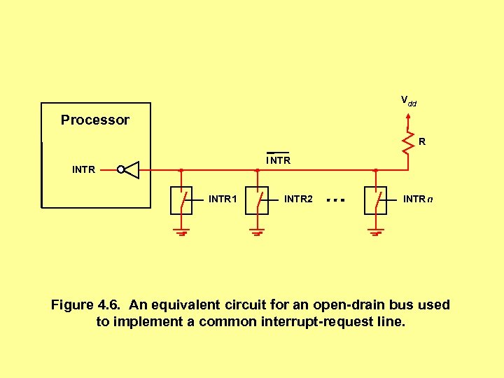
Vdd Processor R I NTR INTR 1 INTR 2 INTR n Figure 4. 6. An equivalent circuit for an open-drain bus used to implement a common interrupt-request line.
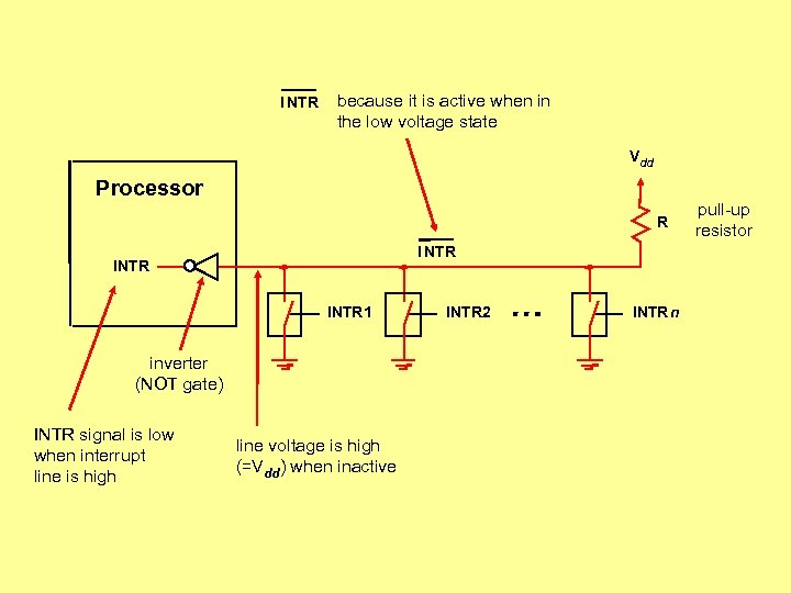
I NTR because it is active when in the low voltage state Vdd Processor R I NTR INTR 1 inverter (NOT gate) INTR signal is low when interrupt line is high line voltage is high (=Vdd) when inactive INTR 2 INTR n pull-up resistor
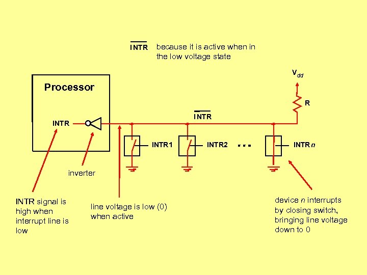
I NTR because it is active when in the low voltage state Vdd Processor R I NTR INTR 1 INTR 2 INTR n inverter INTR signal is high when interrupt line is low line voltage is low (0) when active device n interrupts by closing switch, bringing line voltage down to 0
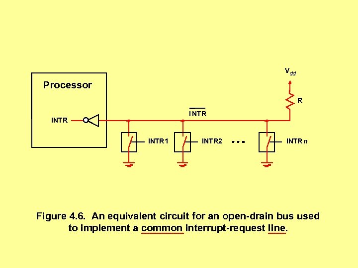
Vdd Processor R I NTR INTR 1 INTR 2 INTR n Figure 4. 6. An equivalent circuit for an open-drain bus used to implement a common interrupt-request line.
Handling Multiple Devices • How can the processor recognize the device requesting an interrupt? • How can the processor obtain the starting address of the appropriate interrupt-service routine? • Should a device be allowed to interrupt the processor while another interrupt is being serviced? • How should two or more simultaneous interrupt requests be handled?
Interrupt Priority • Multi-level priority organization • During execution of interrupt-service routine – Disable interrupts from devices at the same level priority or lower – Continue to accept interrupt requests from higher priority devices – Privileged instructions executed in supervisor mode • Controlling device requests – Interrupt-enable • KEN, DEN
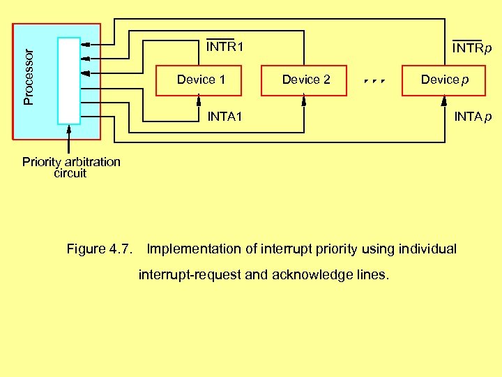
Processor INTR 1 Device 1 I NTRp Device 2 INTA 1 Device p INTA p Priority arbitration circuit Figure 4. 7. Implementation of interrupt priority using individual interrupt-request and acknowledge lines.
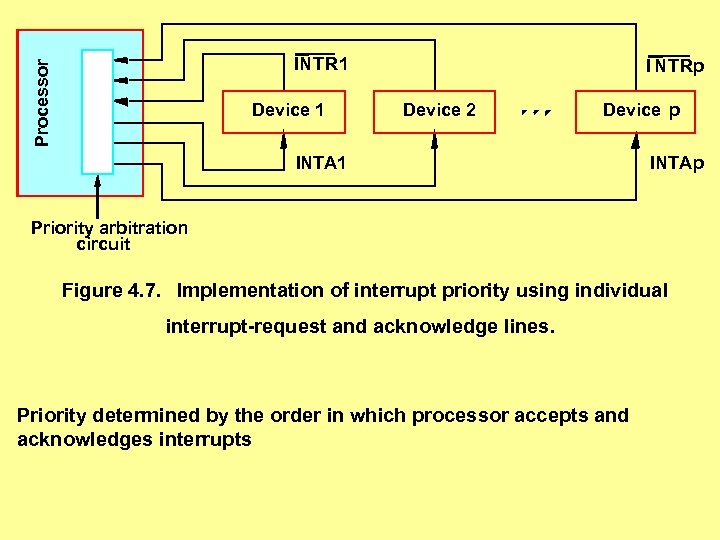
Processor INTR 1 Device 1 I NTRp Device 2 Device p INTA 1 INTAp Priority arbitration circuit Figure 4. 7. Implementation of interrupt priority using individual interrupt-request and acknowledge lines. Priority determined by the order in which processor accepts and acknowledges interrupts
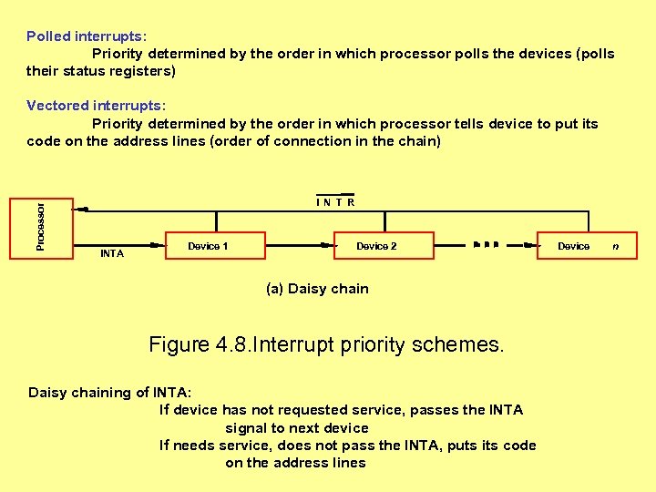
Polled interrupts: Priority determined by the order in which processor polls the devices (polls their status registers) Processor Vectored interrupts: Priority determined by the order in which processor tells device to put its code on the address lines (order of connection in the chain) I N T R INTA Device 1 Device 2 (a) Daisy chain Figure 4. 8. Interrupt priority schemes. Daisy chaining of INTA: If device has not requested service, passes the INTA signal to next device If needs service, does not pass the INTA, puts its code on the address lines Device n
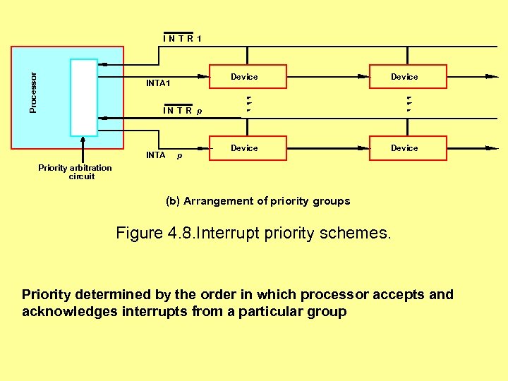
Processor IN TR 1 Device INTA 1 Device IN T R p INTA p Priority arbitration circuit (b) Arrangement of priority groups Figure 4. 8. Interrupt priority schemes. Priority determined by the order in which processor accepts and acknowledges interrupts from a particular group
Multiple Interrupts • Priority in Processor Status Word – Status Register -- active program – Status Word -- inactive program • Changed only by privileged instruction • Mode changes -- automatic or by privileged instruction • Interrupt enable/disable, by device, system-wide
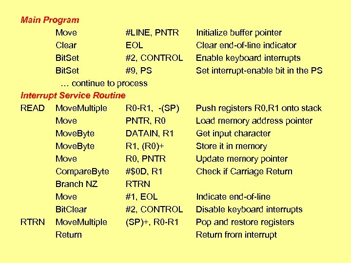
Main Program Move #LINE, PNTR Clear EOL Bit. Set #2, CONTROL Bit. Set #9, PS … continue to process Interrupt Service Routine READ Move. Multiple R 0 -R 1, -(SP) Move PNTR, R 0 Move. Byte DATAIN, R 1 Move. Byte R 1, (R 0)+ Move R 0, PNTR Compare. Byte #$0 D, R 1 Branch NZ RTRN Move #1, EOL Bit. Clear #2, CONTROL RTRN Move. Multiple (SP)+, R 0 -R 1 Return Initialize buffer pointer Clear end-of-line indicator Enable keyboard interrupts Set interrupt-enable bit in the PS Push registers R 0, R 1 onto stack Load memory address pointer Get input character Store it in memory Update memory pointer Check if Carriage Return Indicate end-of-line Disable keyboard interrupts Pop and restore registers Return from interrupt
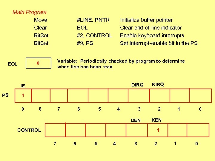
Main Program Move Clear Bit. Set #LINE, PNTR EOL #2, CONTROL #9, PS Variable: Periodically checked by program to determine when line has been read 0 EOL Initialize buffer pointer Clear end-of-line indicator Enable keyboard interrupts Set interrupt-enable bit in the PS DIRQ IE PS KIRQ 1 9 8 7 6 5 4 3 2 DEN KEN CONTROL 1 0 1 7 6 5 4 3 2 1 0
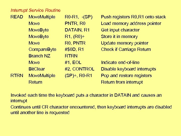
Interrupt Service Routine READ Move. Multiple Move. Byte Move Compare. Byte Branch NZ Move Bit. Clear RTRN Move. Multiple Return R 0 -R 1, -(SP) PNTR, R 0 DATAIN, R 1, (R 0)+ R 0, PNTR #$0 D, R 1 RTRN #1, EOL #2, CONTROL (SP)+, R 0 -R 1 Push registers R 0, R 1 onto stack Load memory address pointer Get input character Store it in memory Update memory pointer Check if Carriage Return Indicate end-of-line Disable keyboard interrupts Pop and restore registers Return from interrupt Invoked each time the keyboard puts a character in DATAIN and causes an interrupt Continues until CR character encountered, then keyboard interrupts are disabled until another line is requested
Interrupt Vectoring Memory Location Address of ISR Interrupt Service Routine Code Address Bus Interrupt Control Bus Device
Common Functions of Interrupts • Interrupt transfers control to the interrupt service routine, generally through the interrupt vector table, which contains the addresses of all the service routines. • Interrupt architecture must save the address of the interrupted instruction and the contents of the processor status register. • Incoming interrupts are disabled while another interrupt is being processed to prevent a lost interrupt. • A software-generated interrupt may be caused either by an error or a user request (sometimes called a trap). • An operating system is interrupt driven.
Interrupts Hardware interrupts—from I/O devices, memory, processor, etc. Software interrupts—generated by a program. Interrupts signal attention requests and error conditions. Interrupts may be intrinsic or user-defined. Other terms: Trap Fault Exception System call IRQ
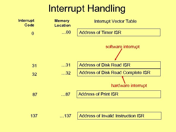
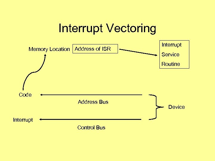
Interrupt Handling Interrupt Code Memory Location 0 … 00 Interrupt Vector Table Address of Timer ISR software interrupt 31 … 31 Address of Disk Read ISR 32 … 32 Address of Disk Read Complete ISR hardware interrupt 87 … 87 137 … 137 Address of Print ISR Address of Invalid Instruction ISR
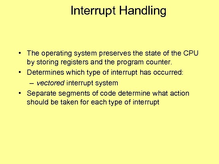
Interrupt Handling • The operating system preserves the state of the CPU by storing registers and the program counter. • Determines which type of interrupt has occurred: – vectored interrupt system • Separate segments of code determine what action should be taken for each type of interrupt
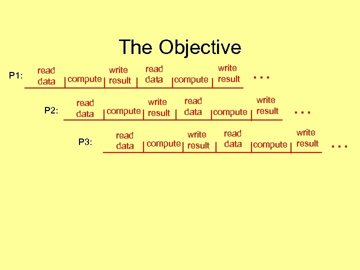
The Objective P 1: read data P 2: write compute result read data P 3: read data write compute result read data compute read data write compute result write result compute read data … write result compute … write result …
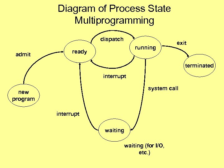
Diagram of Process State Multiprogramming dispatch admit running ready exit terminated interrupt system call new program interrupt waiting (for I/O, etc. )
Process Scheduling Queues • Job queue – set if new programs presented to the system. • Ready queue – set of all processes residing in main memory, ready and waiting to execute. • Device queues – set of processes waiting for an I/O device. • Process migration between the various queues.
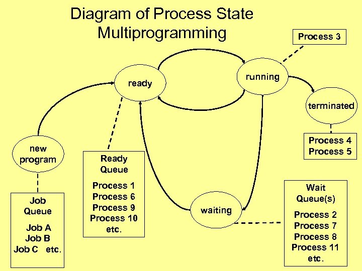
Diagram of Process State Multiprogramming Process 3 running ready terminated new program Job Queue Job A Job B Job C etc. Process 4 Process 5 Ready Queue Process 1 Process 6 Process 9 Process 10 etc. Wait Queue(s) waiting Process 2 Process 7 Process 8 Process 11 etc.
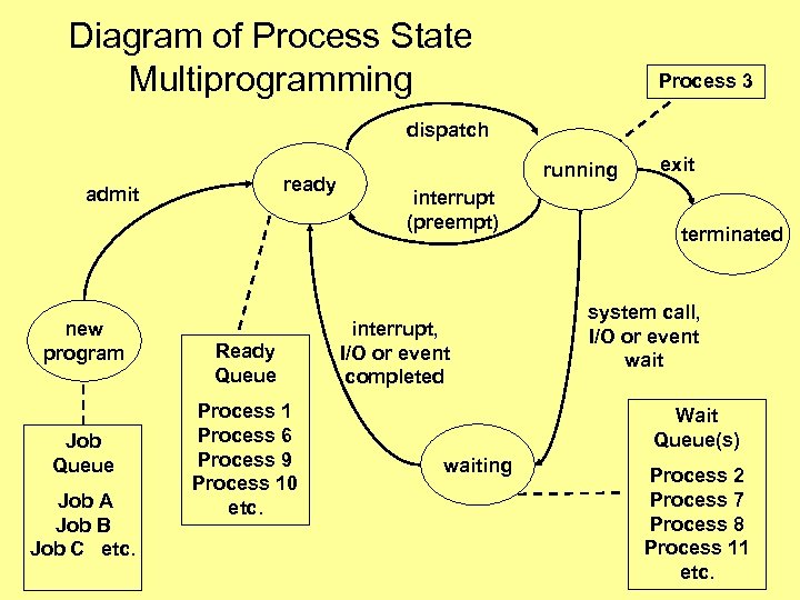
Diagram of Process State Multiprogramming Process 3 dispatch ready admit new program Job Queue Job A Job B Job C etc. Ready Queue Process 1 Process 6 Process 9 Process 10 etc. running interrupt (preempt) interrupt, I/O or event completed exit terminated system call, I/O or event wait Wait Queue(s) waiting Process 2 Process 7 Process 8 Process 11 etc.
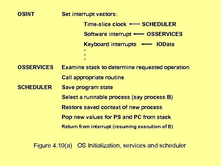
OSINT Set interrupt vectors: Time-slice clock Software interrupt Keyboard interrupts . . . OSSERVICES SCHEDULER OSSERVICES IOData Examine stack to determine requested operation Call appropriate routine SCHEDULER Save program state Select a runnable process (say process B) Restore saved context of new process Pop new values for PS and PC from stack Return from interrupt (resuming execution of B) Figure 4. 10(a) OS Initialization, services and scheduler
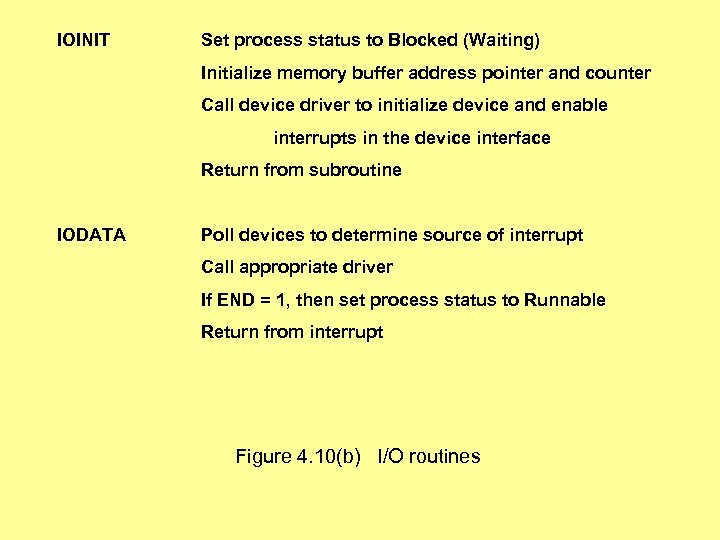
IOINIT Set process status to Blocked (Waiting) Initialize memory buffer address pointer and counter Call device driver to initialize device and enable interrupts in the device interface Return from subroutine IODATA Poll devices to determine source of interrupt Call appropriate driver If END = 1, then set process status to Runnable Return from interrupt Figure 4. 10(b) I/O routines
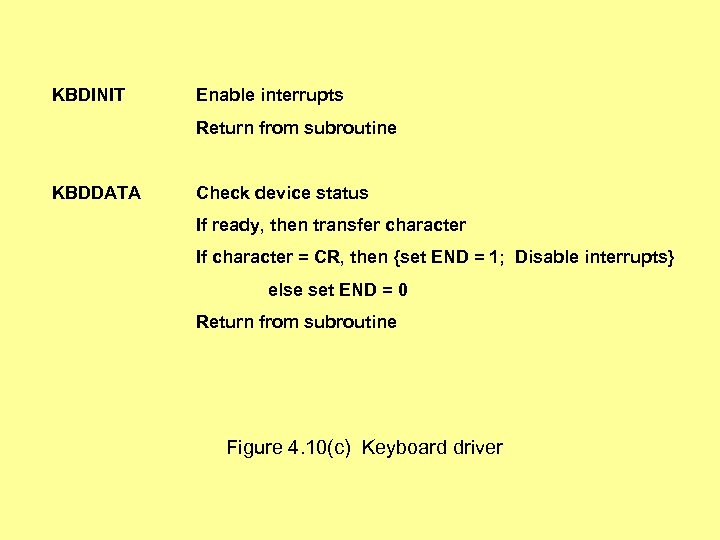
KBDINIT Enable interrupts Return from subroutine KBDDATA Check device status If ready, then transfer character If character = CR, then {set END = 1; Disable interrupts} else set END = 0 Return from subroutine Figure 4. 10(c) Keyboard driver
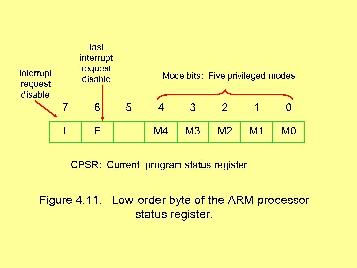
fast interrupt request disable Interrupt request disable 7 6 I F Mode bits: Five privileged modes 5 4 3 2 1 0 M 4 M 3 M 2 M 1 M 0 CPSR: Current program status register Figure 4. 11. Low-order byte of the ARM processor status register.
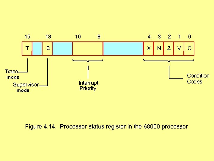
15 13 T 10 8 S mode Supervisor mode Interrupt Priority 3 2 1 0 X Trace 4 N Z V C Condition Codes Figure 4. 14. Processor status register in the 68000 processor.
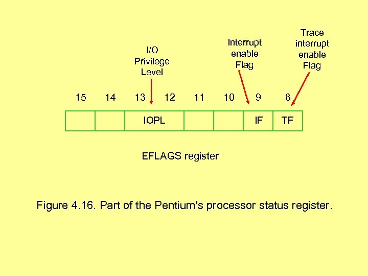
Interrupt enable Flag I/O Privilege Level 15 14 13 12 Trace interrupt enable Flag 11 IOPL 10 9 8 IF TF EFLAGS register Figure 4. 16. Part of the Pentium's processor status register.
Direct Memory Access (DMA) • Polling or interrupt driven I/O incurs considerable overhead – Multiple program instructions – Saving program state – Incrementing memory addresses – Keeping track of word count • Transfer large amounts of data at high speed without continuous intervention by the processor • Special control circuit required in the I/O device interface, called a DMA controller • DMA controller keeps track of memory locations, transfers directly to memory (via the bus) independent of the processor
DMA Controller • Part of the I/O device interface – DMA Channels • Performs functions that would normally be carried out by the processor – Provides memory address – Bus signals that control transfer – Keeps track of number of transfers • Under control of the processor
Direct Memory Access (DMA) • OS responds to a program’s system call for Disk Read, for example • OS puts the program in the “blocked” or “waiting” or “asleep” state • Initiates the Disk Read • Starts execution of another program • When Read is completed, DMA controller sends an interrupt
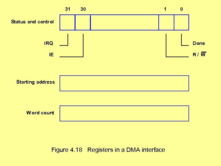
31 30 1 0 Status and control IRQ Done IE R/ W Starting address W ord count Figure 4. 18 Re gisters in DMA interf ace. Registersin aa DMA interface
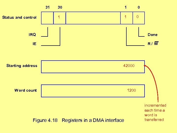
31 Status and control 30 1 1 0 IRQ Done IE R/ W Starting address W ord count 42000 1200 Figure 4. 18 Re gisters in a DMA interface ace. Figure 4. 18. Registers in a DMA interf incremented each time a word is transferred
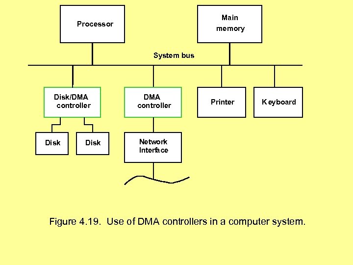
Main memory Processor System bus Disk/DMA controller Disk DMA controller Printer K eyboard Network Interface Figure 4. 19. Use of DMA controllers in incomputer system. Figure 4. 19. Use of DMA controllers a a computer system.
DMA • Processor and DMA controller(s) must “interweave” memory accesses • DMA controllers have higher priority for obvious reason, i. e. , higher speed devices need higher priority
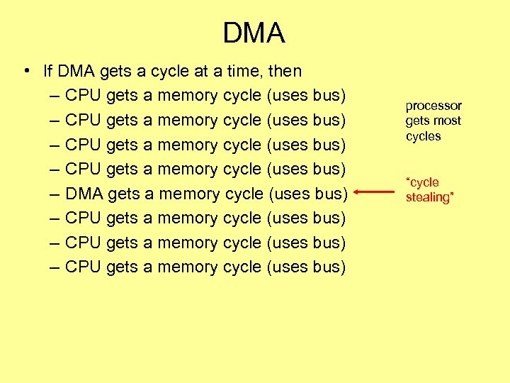
DMA • If DMA gets a cycle at a time, then – CPU gets a memory cycle (uses bus) – DMA gets a memory cycle (uses bus) – CPU gets a memory cycle (uses bus) processor gets most cycles “cycle stealing”
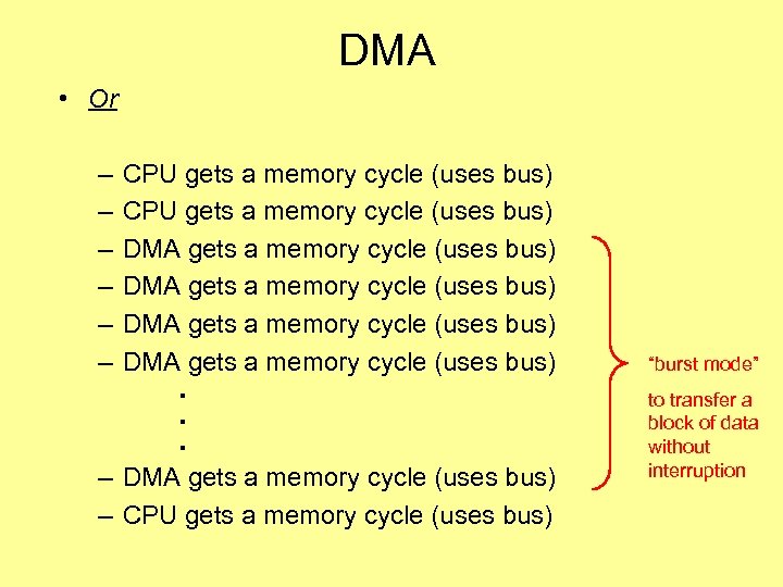
DMA • Or – – – CPU gets a memory cycle (uses bus) DMA gets a memory cycle (uses bus) . . . – DMA gets a memory cycle (uses bus) – CPU gets a memory cycle (uses bus) “burst mode” to transfer a block of data without interruption
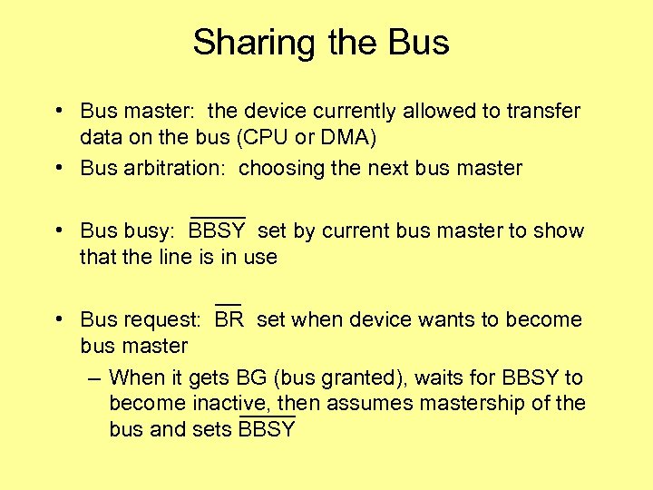
Sharing the Bus • Bus master: the device currently allowed to transfer data on the bus (CPU or DMA) • Bus arbitration: choosing the next bus master • Bus busy: BBSY set by current bus master to show that the line is in use • Bus request: BR set when device wants to become bus master – When it gets BG (bus granted), waits for BBSY to become inactive, then assumes mastership of the bus and sets BBSY
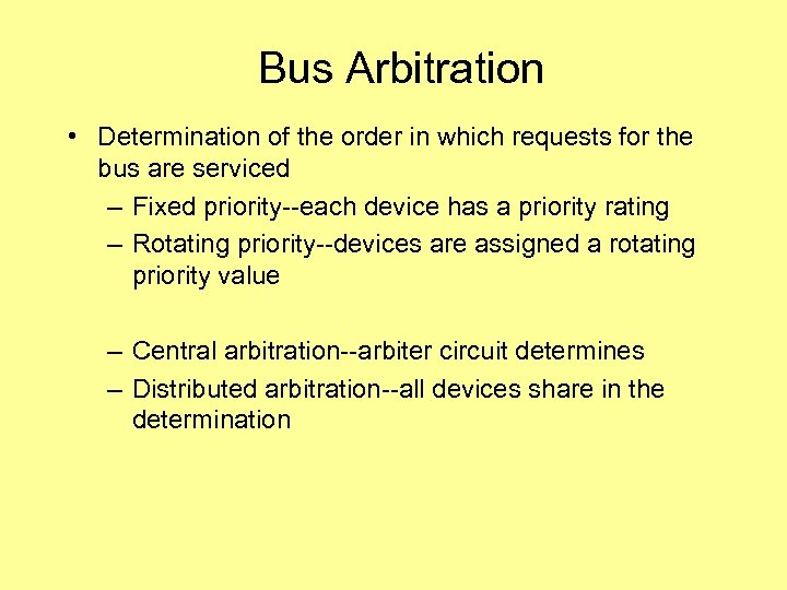
Bus Arbitration • Determination of the order in which requests for the bus are serviced – Fixed priority--each device has a priority rating – Rotating priority--devices are assigned a rotating priority value – Central arbitration--arbiter circuit determines – Distributed arbitration--all devices share in the determination
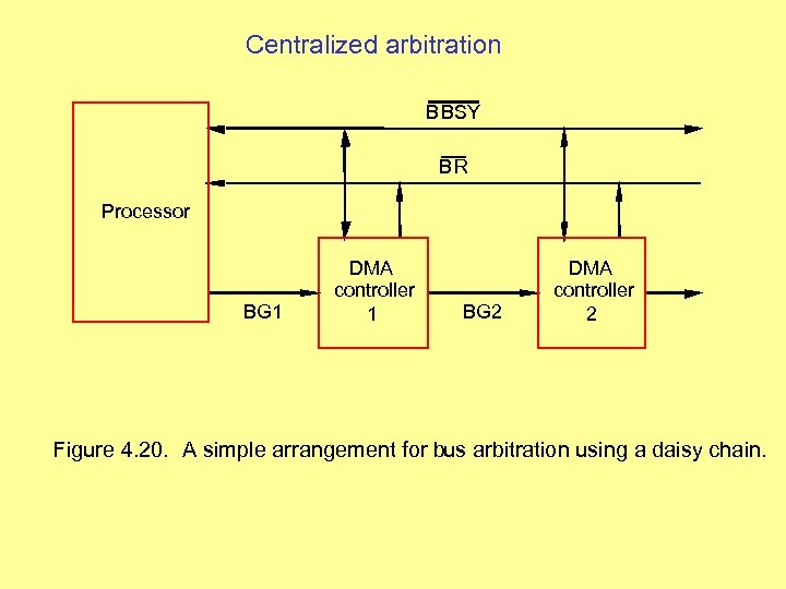
Centralized arbitration B BSY BR Processor BG 1 DMA controller 1 BG 2 DMA controller 2 Figure 4. 20. A simple arrangement for bus arbitration using a daisy chain.
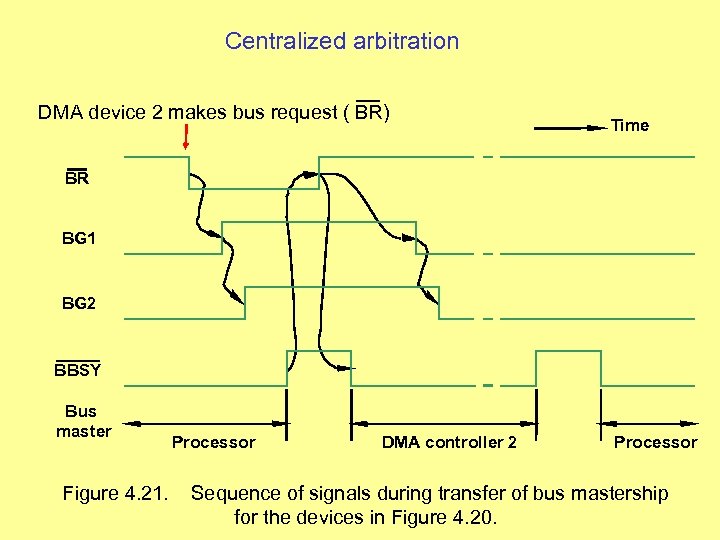
Centralized arbitration DMA device 2 makes bus request ( BR) Time BR BG 1 BG 2 BBSY Bus master Figure 4. 21. Processor DMA controller 2 Processor Sequence of signals during transfer of bus mastership for the devices in Figure 4. 20.
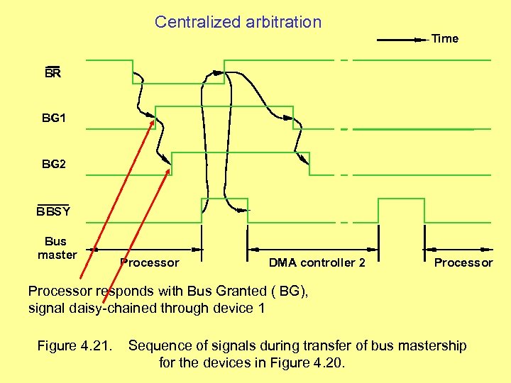
Centralized arbitration Time BR BG 1 BG 2 BBSY Bus master Processor DMA controller 2 Processor responds with Bus Granted ( BG), signal daisy-chained through device 1 Figure 4. 21. Sequence of signals during transfer of bus mastership for the devices in Figure 4. 20.
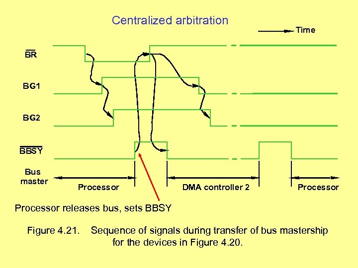
Centralized arbitration Time BR BG 1 BG 2 BBSY Bus master Processor DMA controller 2 Processor releases bus, sets BBSY Figure 4. 21. Sequence of signals during transfer of bus mastership for the devices in Figure 4. 20.
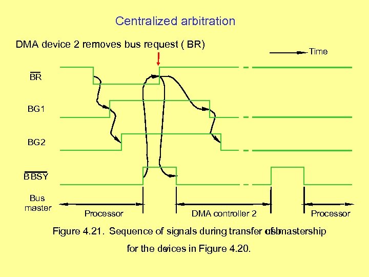
Centralized arbitration DMA device 2 removes bus request ( BR) Time BR BG 1 BG 2 B BSY Bus master Processor DMA controller 2 Processor Figure 4. 21. Sequence of signals during transfer of b us mastership for the de vices in Figure 4. 20.
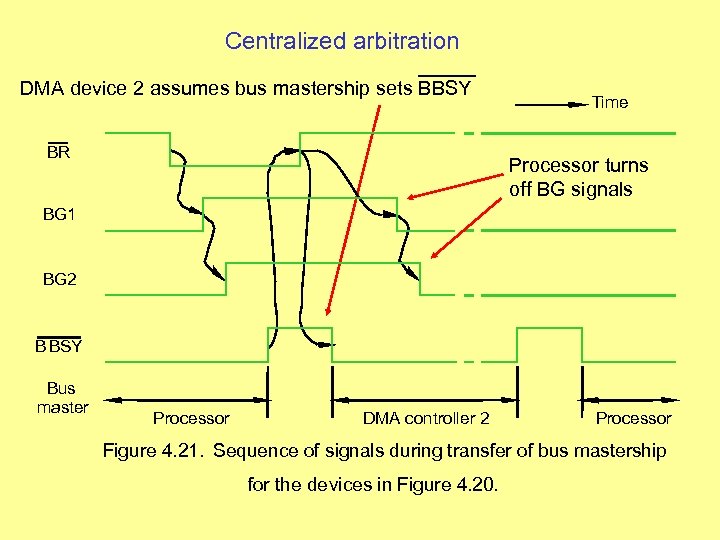
Centralized arbitration DMA device 2 assumes bus mastership sets BBSY BR Time Processor turns off BG signals BG 1 BG 2 B BSY Bus master Processor DMA controller 2 Processor Figure 4. 21. Sequence of signals during transfer of bus mastership for the devices in Figure 4. 20.
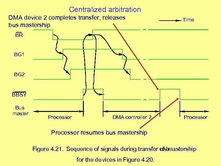
Centralized arbitration DMA device 2 completes transfer, releases bus mastership Time BR BG 1 BG 2 B BSY Bus master Processor DMA controller 2 Processor resumes bus mastership Figure 4. 21. Sequence of signals during transfer of b us mastership for the de vices in Figure 4. 20.
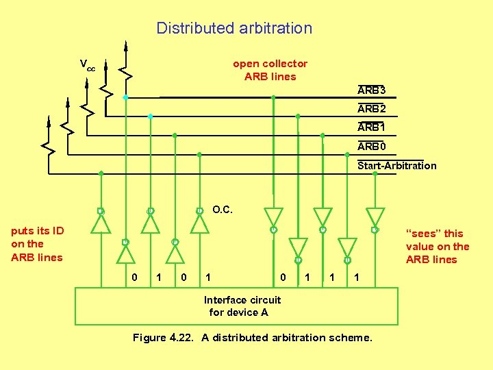
Distributed arbitration open collector ARB lines Vcc ARB 3 ARB 2 ARB 1 ARB 0 Start-Arbitration O. C. puts its ID on the ARB lines “sees” this value on the ARB lines 0 1 0 1 1 1 Interface circuit for device A Figure 4. 22. A distributed arbitration scheme.
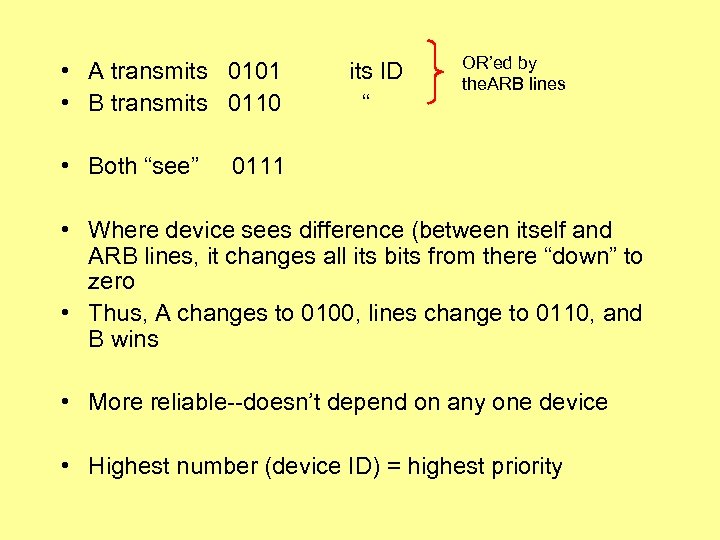
• A transmits 0101 • B transmits 0110 • Both “see” its ID “ OR’ed by the. ARB lines 0111 • Where device sees difference (between itself and ARB lines, it changes all its bits from there “down” to zero • Thus, A changes to 0100, lines change to 0110, and B wins • More reliable--doesn’t depend on any one device • Highest number (device ID) = highest priority
Synchronous Bus • All devices clocked by a common clock line • Signals sent or data transferred at equally spaced intervals • Bus clock is not necessarily the same as the internal CPU clock (bus clock is slower, of course)
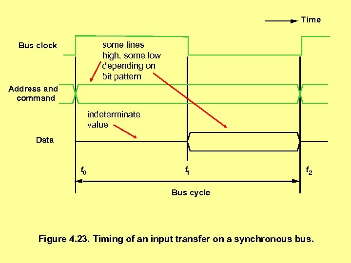
Time some lines high, some low depending on bit pattern Bus clock Address and command indeterminate value Data t 0 t 1 t 2 Bus cycle Figure 4. 23. Timing of an input transfer on a synchronous bus.
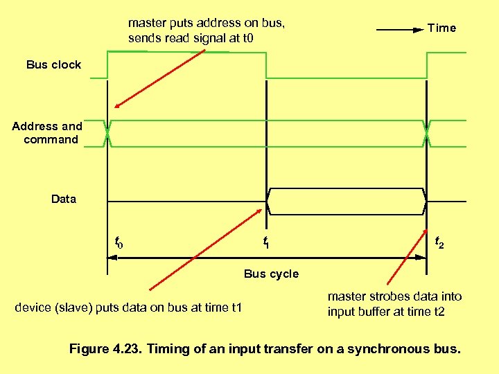
master puts address on bus, sends read signal at t 0 Time Bus clock Address and command Data t 0 t 1 t 2 Bus cycle device (slave) puts data on bus at time t 1 master strobes data into input buffer at time t 2 Figure 4. 23. Timing of an input transfer on a synchronous bus.
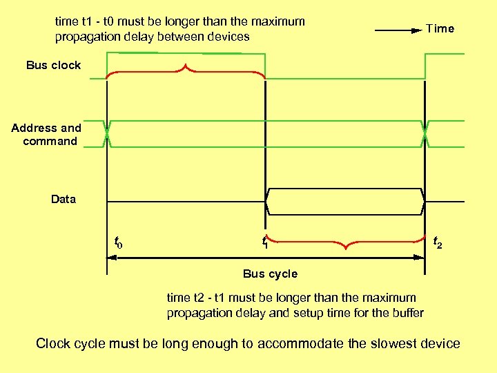
time t 1 - t 0 must be longer than the maximum propagation delay between devices Time Bus clock Address and command Data t 0 t 1 t 2 Bus cycle time t 2 - t 1 must be longer than the maximum propagation delay and setup time for the buffer Clock cycle must be long enough to accommodate the slowest device
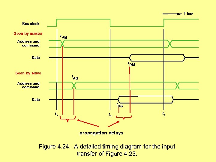
T ime Bus clock Seen by master t Address and command AM Data t Seen by slave DM t AS Address and command Data t DS t 0 t 1 t 2 propagation delays Figure 4. 24. A detailed timing diagram for the input transfer of Figure 4. 23.
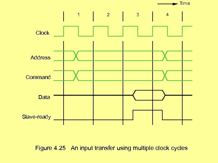
Time 1 2 3 4 Clock Address Command Data Slave-ready Figure 4. 25 An input transfer using multiple clock cycles
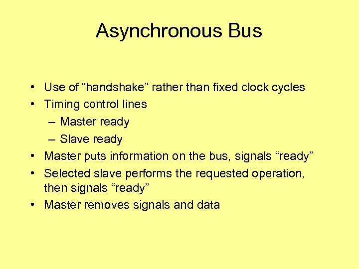
Asynchronous Bus • Use of “handshake” rather than fixed clock cycles • Timing control lines – Master ready – Slave ready • Master puts information on the bus, signals “ready” • Selected slave performs the requested operation, then signals “ready” • Master removes signals and data
Bus “Skew” • Master puts address and read signal on the bus at time t 0 • Waits (until time t 1) to allow for address decoding and bus skew – (Not all lines have the same propagation speed) • Master signals “master ready” at time t 1
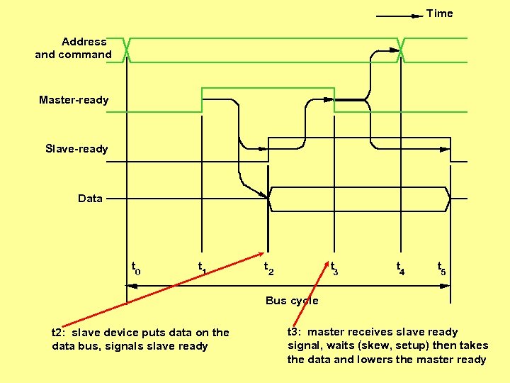
Time Address and command Master-ready Slave-ready Data t 0 t 1 t 2 t 3 t 4 t 5 Bus cycle t 2: slave device puts data on the data bus, signals slave ready t 3: master receives slave ready signal, waits (skew, setup) then takes the data and lowers the master ready
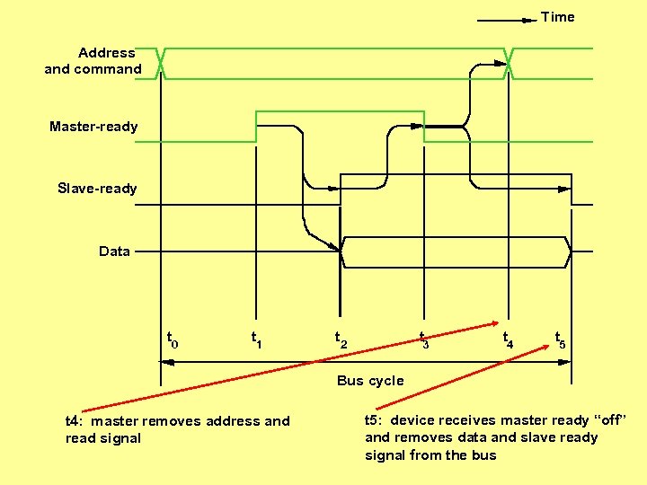
Time Address and command Master-ready Slave-ready Data t 0 t 1 t 2 t 3 t 4 t 5 Bus cycle t 4: master removes address and read signal t 5: device receives master ready “off” and removes data and slave ready signal from the bus
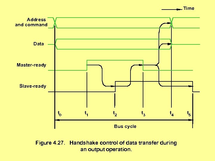
Time Address and command Data Master-ready Slave-ready t 0 t 1 t 2 t 3 t 4 Bus cycle Figure 4. 27. Handshake control of data transfer during an output operation. t 5
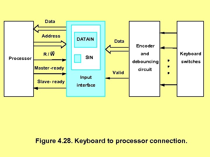
Data Address Processor R/W DATAIN Input Encoder and Valid Keyboard debouncing SIN Master -ready Slave- ready Data switches circuit interface Figure 4. 28. Keyboard to processor connection.
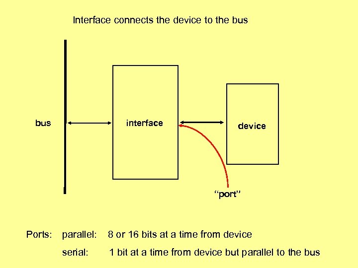
Interface connects the device to the bus interface device “port” Ports: parallel: serial: 8 or 16 bits at a time from device 1 bit at a time from device but parallel to the bus
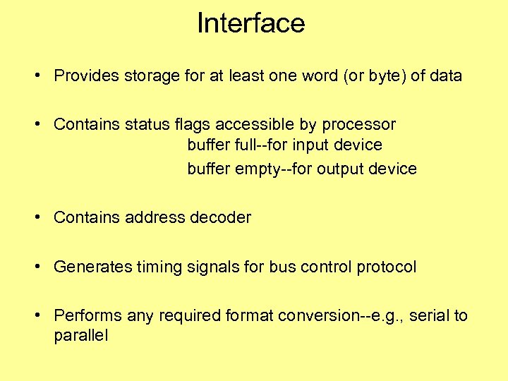
Interface • Provides storage for at least one word (or byte) of data • Contains status flags accessible by processor buffer full--for input device buffer empty--for output device • Contains address decoder • Generates timing signals for bus control protocol • Performs any required format conversion--e. g. , serial to parallel
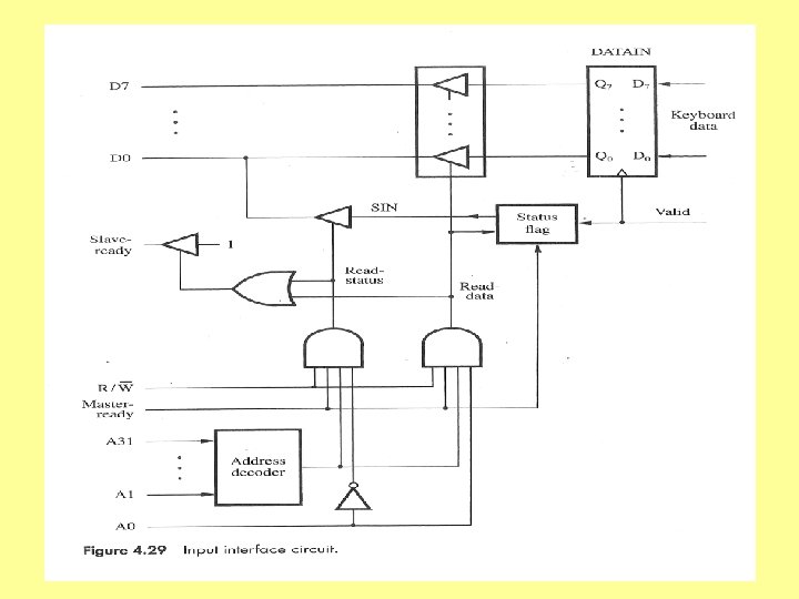
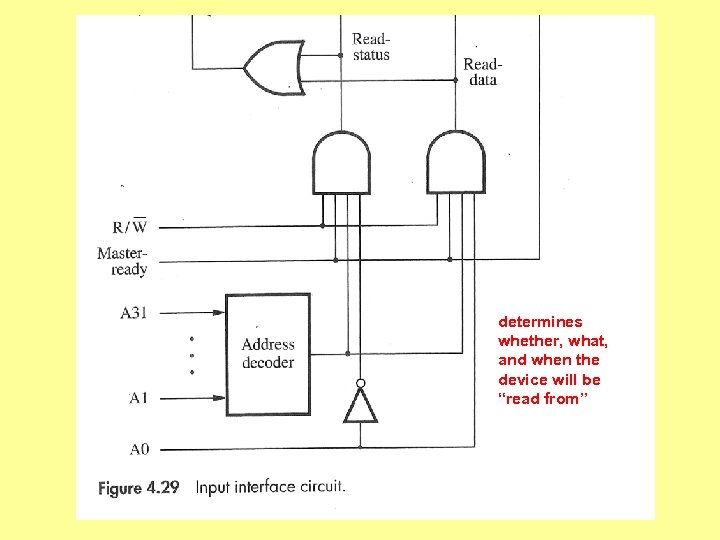
determines whether, what, and when the device will be “read from”
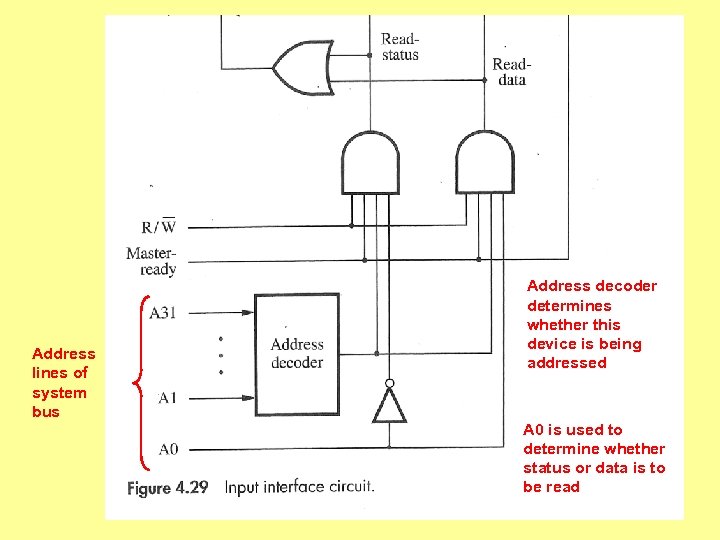
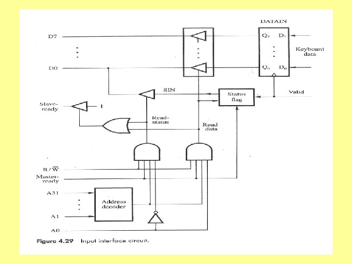
Address lines of system bus Address decoder determines whether this device is being addressed A 0 is used to determine whether status or data is to be read
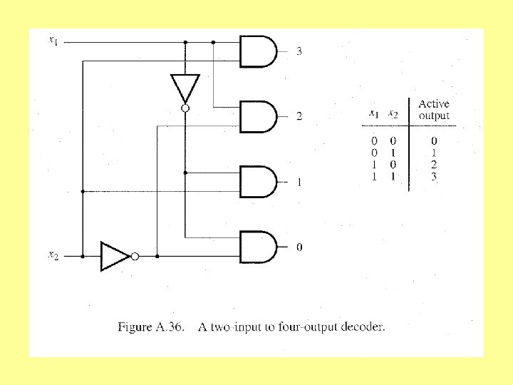
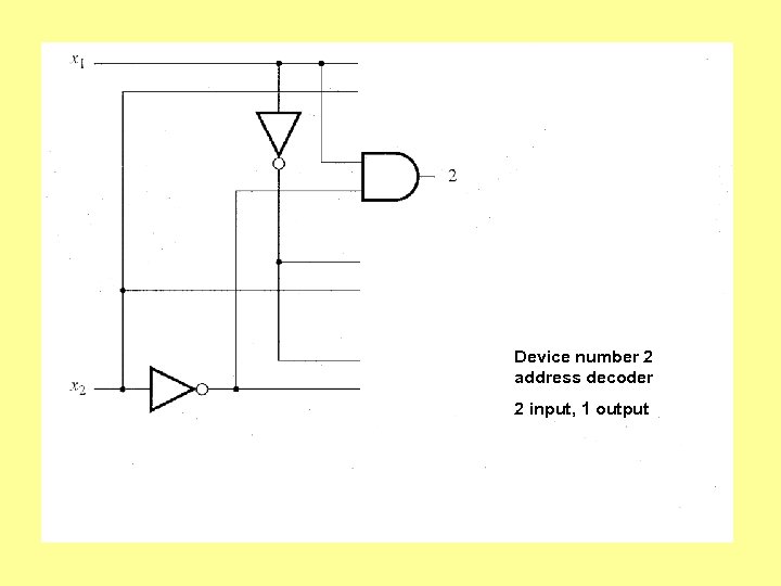
Device number 2 address decoder 2 input, 1 output
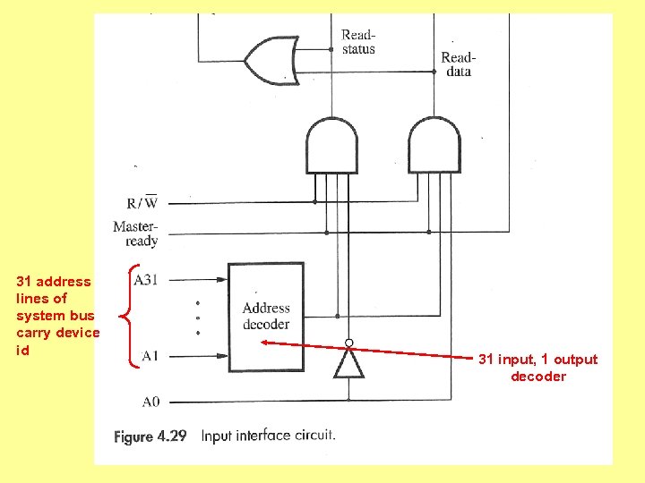
31 address lines of system bus carry device id 31 input, 1 output decoder
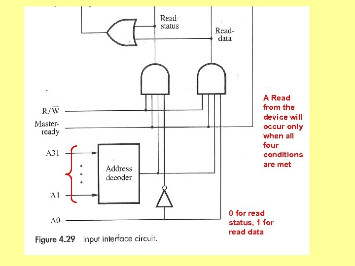
A Read from the device will occur only when all four conditions are met 0 for read status, 1 for read data
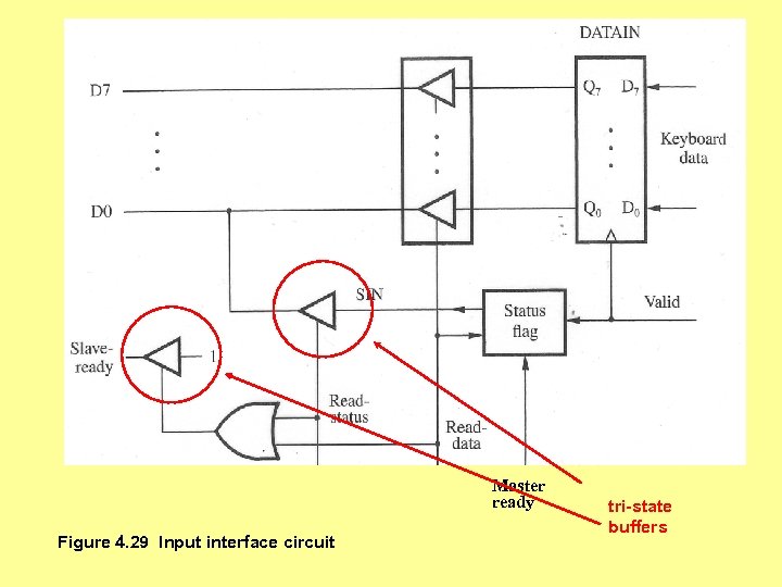
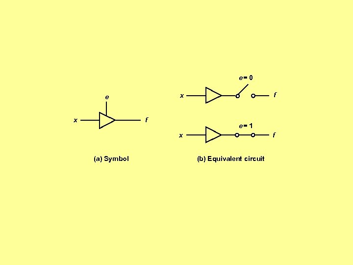
Master ready Figure 4. 29 Input interface circuit tri-state buffers
e= 0 x f x e f e= 1 x (a) Symbol f (b) Equivalent circuit
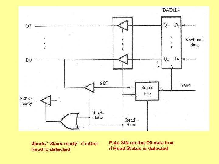
Sends “Slave-ready” if either Read is detected Puts SIN on the D 0 data line if Read Status is detected
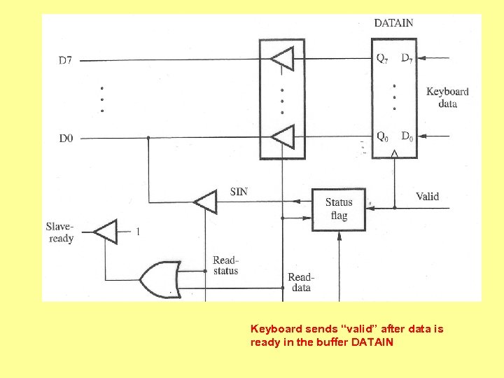
Keyboard sends “valid” after data is ready in the buffer DATAIN
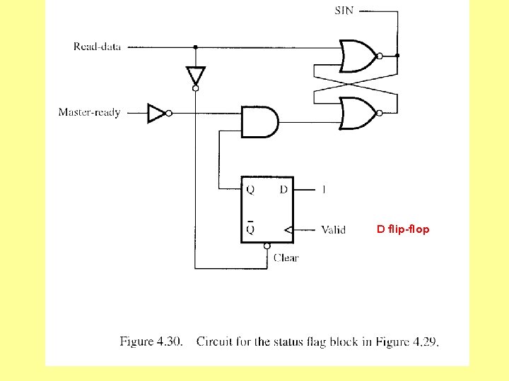
D flip-flop
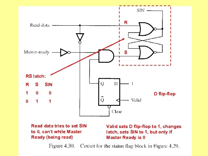
R S RS latch: R S SIN 1 0 0 0 1 1 Read data tries to set SIN to 0, can’t while Master Ready (being read) D flip-flop Valid sets D flip-flop to 1, changes latch, sets SIN to 1, but only if Master Ready is 0
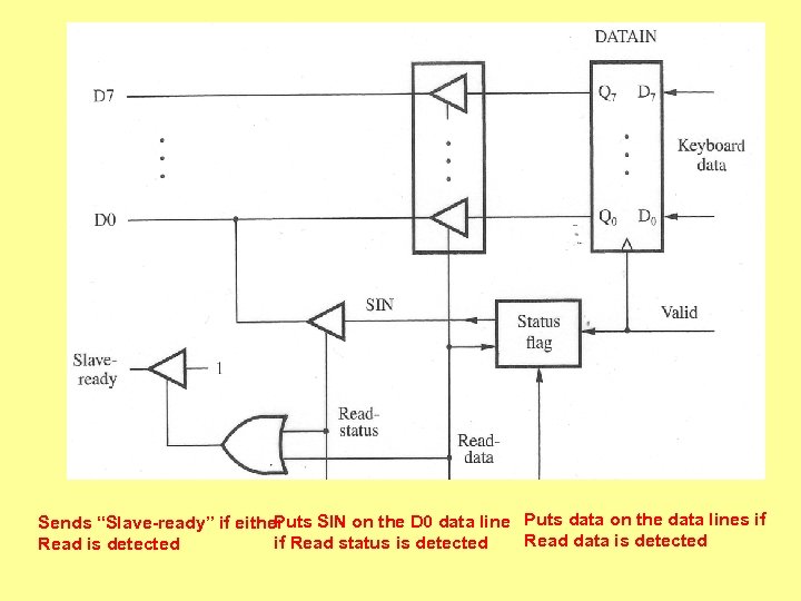
Puts SIN on the D 0 data line Puts data on the data lines if Sends “Slave-ready” if either Read data is detected if Read status is detected Read is detected
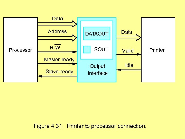
Data Address Processor CPU R-W DATAOUT Data SOUT Valid Output interface Idle Master-ready Slave-ready Figure 4. 31. Printer to processor connection. Printer


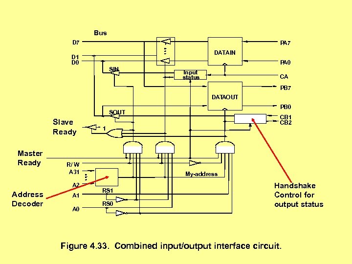
Bus D 7 PA 7 DATAIN D 1 D 0 PA 0 SIN Input status CA PB 7 DATAOUT PB 0 SOUT Slave Ready Master Ready Address Decoder 1 R/ W A 31 A 2 A 1 A 0 CB 1 CB 2 My-address RS 1 RS 0 Handshake Control for output status Figure 4. 33. Combined input/output interface circuit.
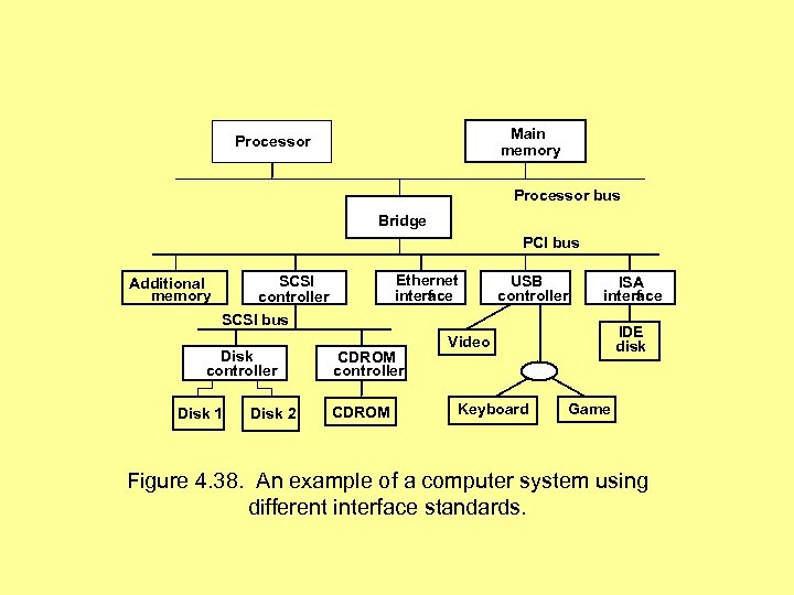
Main memory Processor bus Bridge PCI bus Ethernet interf ce a SCSI controller Additional memory USB controller ISA interf ce a SCSI bus Disk controller Disk 1 Disk 2 CDROM controller CDROM IDE disk Video Keyboard Game Figure 4. 38. An example of a computer system using different interface standards.
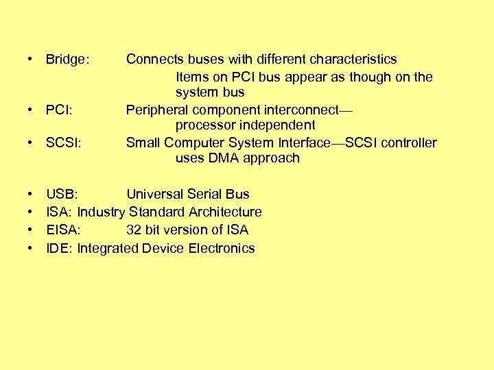
• Bridge: • PCI: • SCSI: • • Connects buses with different characteristics Items on PCI bus appear as though on the system bus Peripheral component interconnect— processor independent Small Computer System Interface—SCSI controller uses DMA approach USB: Universal Serial Bus ISA: Industry Standard Architecture EISA: 32 bit version of ISA IDE: Integrated Device Electronics
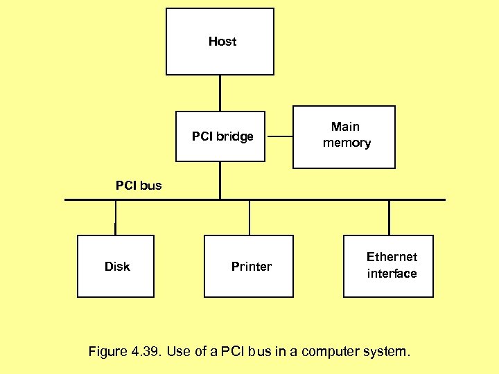
Host PCI bridge Main memory PCI bus Disk Printer Ethernet interface Figure 4. 39. Use of a PCI bus in a computer system.
USB Interface • Need for high transfer rates • Need devices at some distance • High rate wide bus? – Problem over distance because of skew • Serial transmission – Low cost and flexible – No skew, so high rates OK, distance OK
USB Interface • Hubs have multiple ports • Devices connect to a port • Hubs connect to a port • “Tree structure”
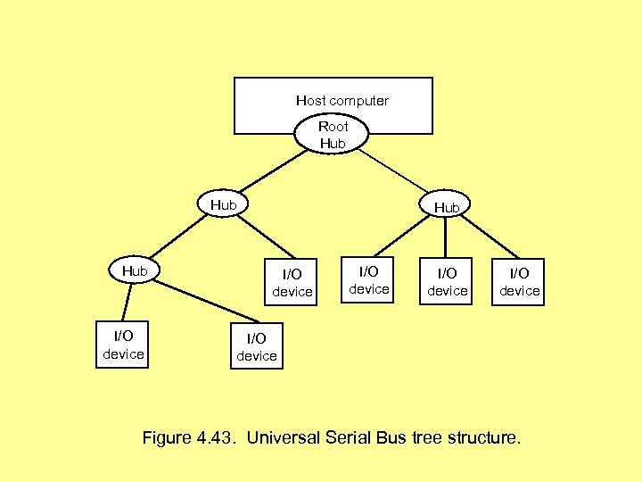
Host computer Root Hub Hub I/O device I/O device Figure 4. 43. Universal Serial Bus tree structure.
USB Interface • Message from host copied to all hubs, to all ports, to all devices • Only the addressed device responds • Message from device only goes “upstream”--up the tree • Makes possible a large number of devices through a few ports at the root hub. • High speed, long distances possible
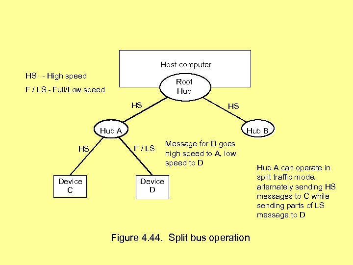
Host computer HS - High speed Root Hub F / LS - Full/Low speed HS HS Hub A HS Device C Hub B F / LS Message for D goes high speed to A, low speed to D Device D Figure 4. 44. Split bus operation Hub A can operate in split traffic mode, alternately sending HS messages to C while sending parts of LS message to D
USB • Data is transmitted in packets of one or more bytes • First field is always a PID (packet id) – A 4 bit ID plus the complement for verification – Therefore, 16 different packet types • Control packets such as ACK are PID only • Token packets used for control • Data packets
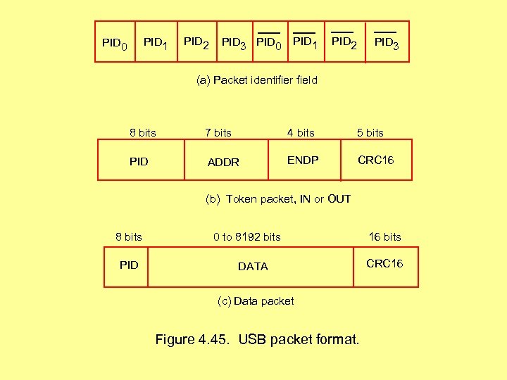
PID 1 PID 0 PID 2 PID 3 PID 0 PID 1 PID 2 PID 3 (a) Packet identifier field 8 bits 7 bits 4 bits 5 bits PID ADDR ENDP CRC 16 (b) Token packet, IN or OUT 8 bits PID 0 to 8192 bits DATA (c) Data packet Figure 4. 45. USB packet format. 16 bits CRC 16
• ADDR: The address, a 7 bit device address (address is local to the USB tree) • ENDP: The endpoint, the location within the device (status register, data register, etc. ) • Data packet follows a token packet containing the address and endpoint of the device. • Packet IDs contain bit that alternates between 0 and 1 to guard against lost packets
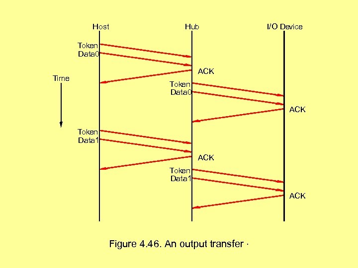
Host Hub I/O Device Token Data 0 ACK Time Token Data 0 ACK Token Data 1 ACK Figure 4. 46. An output transfer .
USB • Software (in host computer) sends packets to devices (hubs just forward them) • Host software periodically polls each hub – New device when connected has address 0 – If a new device has been added, host collects info about the device from the memory of the device and assigns it a 7 bit address • Locations within the device (registers) are identified by a 4 bit endpoint address
d097fb8c16f58f6b0d3fd061511db3c2.ppt