a8e700fd07db557a725867742ce9ef57.ppt
- Количество слайдов: 73
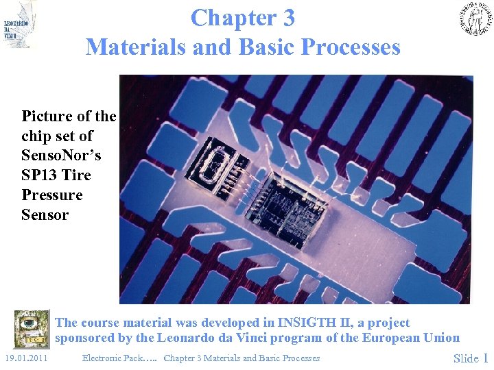
Chapter 3 Materials and Basic Processes Picture of the chip set of Senso. Nor’s SP 13 Tire Pressure Sensor The course material was developed in INSIGTH II, a project sponsored by the Leonardo da Vinci program of the European Union 19. 01. 2011 Electronic Pack…. . Chapter 3 Materials and Basic Processes Slide 1
Materials: Metals • Right choice, right use and compatibility of materials is the key to good packaging and optimal properties. – Elemental metals: • High electrical conductivity • High thermal conductivity • Higher thermal coefficient of expansion (TCE) than semiconductors and most ceramics – Alloys: taylored to many uses: • Poorer electrical and thermal conductivity than elements • Taylored TCE • Lower melting point 19. 01. 2011 Electronic Pack…. . Chapter 3 Materials and Basic Processes Slide 2
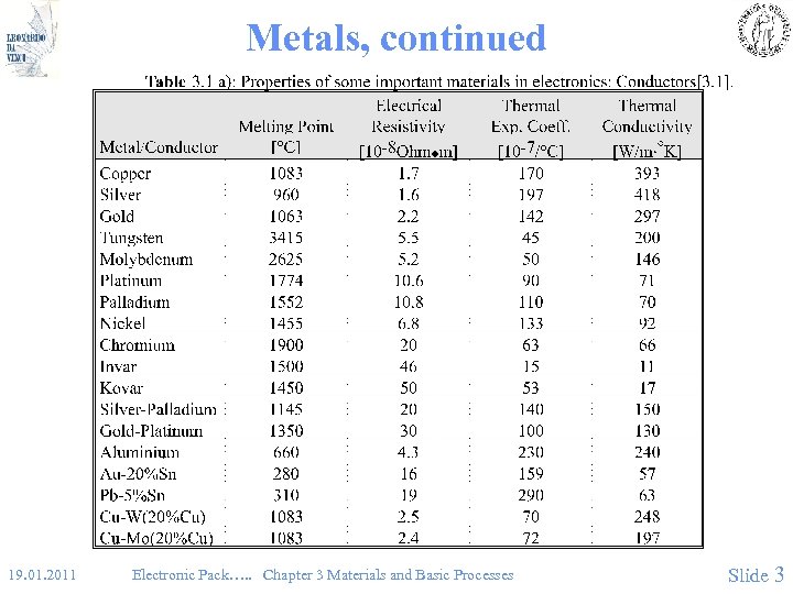
Metals, continued • (Table 3. 1) 19. 01. 2011 Electronic Pack…. . Chapter 3 Materials and Basic Processes Slide 3
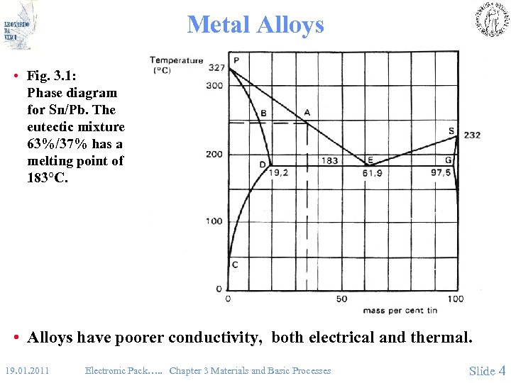
Metal Alloys • Fig. 3. 1: Phase diagram for Sn/Pb. The eutectic mixture 63%/37% has a melting point of 183°C. • Alloys have poorer conductivity, both electrical and thermal. 19. 01. 2011 Electronic Pack…. . Chapter 3 Materials and Basic Processes Slide 4
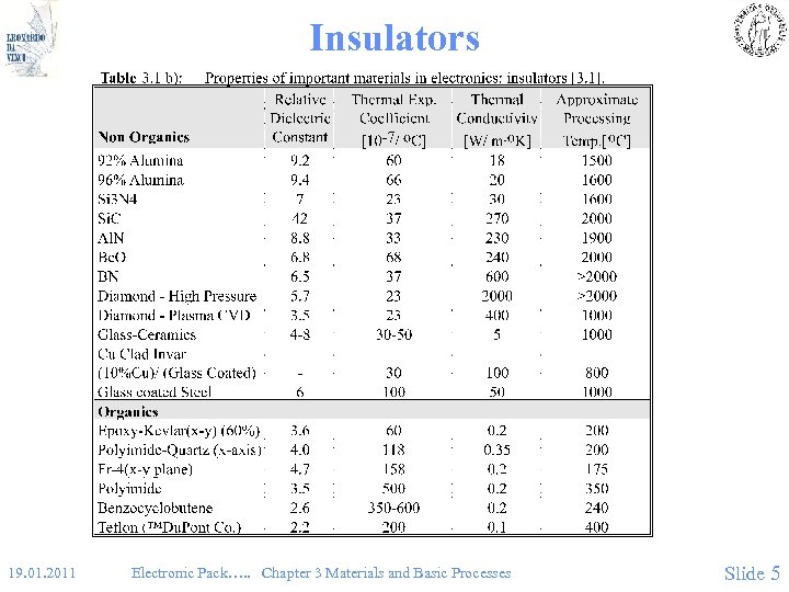
Insulators • (Fig 3. 1 b) 19. 01. 2011 Electronic Pack…. . Chapter 3 Materials and Basic Processes Slide 5
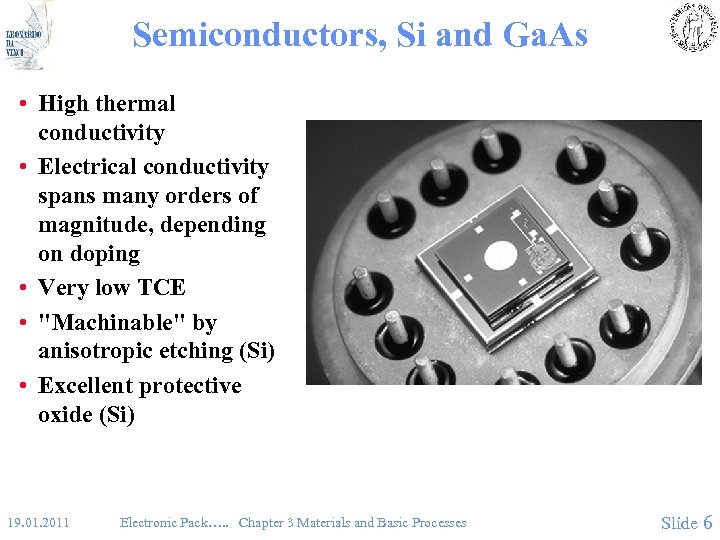
Semiconductors, Si and Ga. As • High thermal conductivity • Electrical conductivity spans many orders of magnitude, depending on doping • Very low TCE • "Machinable" by anisotropic etching (Si) • Excellent protective oxide (Si) 19. 01. 2011 Electronic Pack…. . Chapter 3 Materials and Basic Processes Slide 6
Ceramics • Inorganic, non-metallic • Made by powder, compressing or tape casting, and high temperature treatment (600 -1800 o. C) • Chemically and thermally very stable • Electrical insulators • Some ceramics are very good thermal conductors 19. 01. 2011 Electronic Pack…. . Chapter 3 Materials and Basic Processes Slide 7
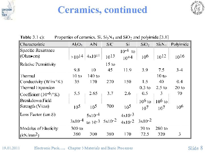
Ceramics, continued 19. 01. 2011 Electronic Pack…. . Chapter 3 Materials and Basic Processes Slide 8
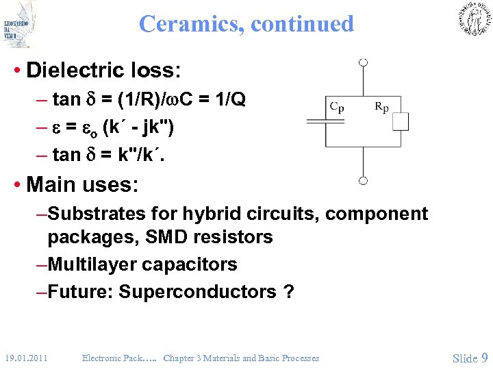
Ceramics, continued • Dielectric loss: – tan = (1/R)/w. C = 1/Q – = o (k´ - jk") – tan = k"/k´. • Main uses: –Substrates for hybrid circuits, component packages, SMD resistors –Multilayer capacitors –Future: Superconductors ? 19. 01. 2011 Electronic Pack…. . Chapter 3 Materials and Basic Processes Slide 9
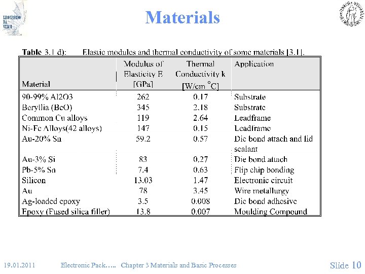
Materials • Fig 3. 1. d 19. 01. 2011 Electronic Pack…. . Chapter 3 Materials and Basic Processes Slide 10
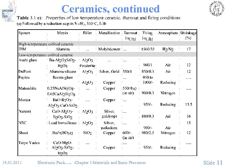
Ceramics, continued 19. 01. 2011 Electronic Pack…. . Chapter 3 Materials and Basic Processes Slide 11
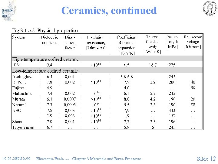
Ceramics, continued 19. 01. 2011 07. 10. 99 Electronic Pack…. . Chapter 3 Materials and Basic Processes Slide 12
Glasses: • Glasses are amorphous, supercooled liquids – Uses: • Matrix for thick film pastes • Hermetic seals • Substrates, together with ceramics 19. 01. 2011 Electronic Pack…. . Chapter 3 Materials and Basic Processes Slide 13
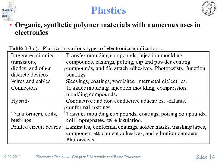
Plastics • Organic, synthetic polymer materials with numerous uses in electronics 19. 01. 2011 Electronic Pack…. . Chapter 3 Materials and Basic Processes Slide 14
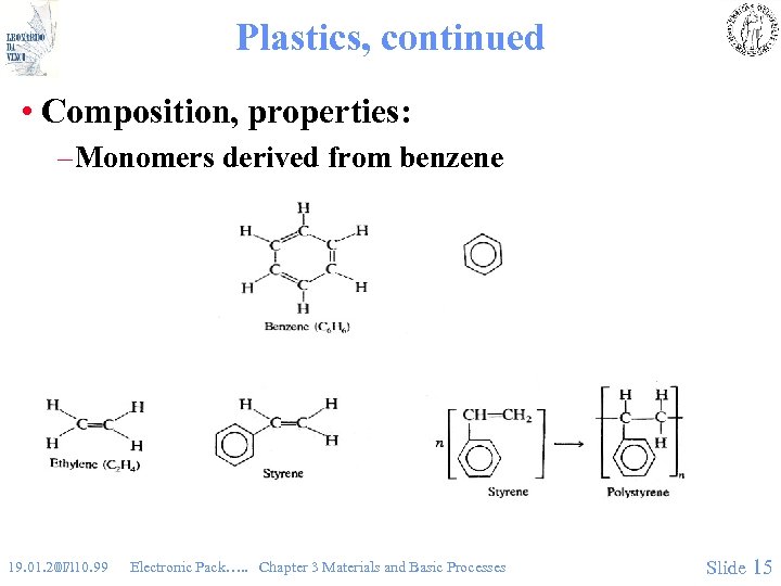
Plastics, continued • Composition, properties: – Monomers derived from benzene 19. 01. 2011 07. 10. 99 Electronic Pack…. . Chapter 3 Materials and Basic Processes Slide 15
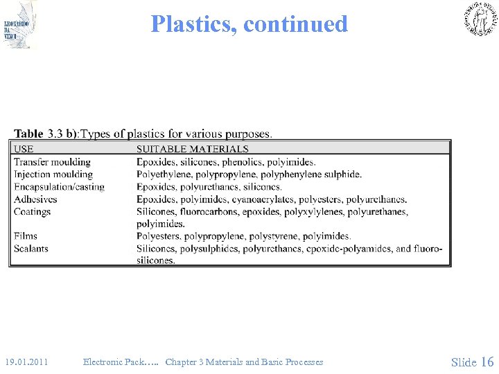
Plastics, continued 19. 01. 2011 Electronic Pack…. . Chapter 3 Materials and Basic Processes Slide 16
Plastics, continued • Requirements: – High electrical resistivity, high breakdown field, low dielectric losses, low dielectric constant – Thermal and mechanical stability – Thermal expansion compatible with Si and metals – High mechanical strength/softness and flexibility – Chemical resistance – Good adhesion to other materials – Ease of processing – Low water absorption, small changes of the properties during the effect of moisture. 19. 01. 2011 Electronic Pack…. . Chapter 3 Materials and Basic Processes Slide 17
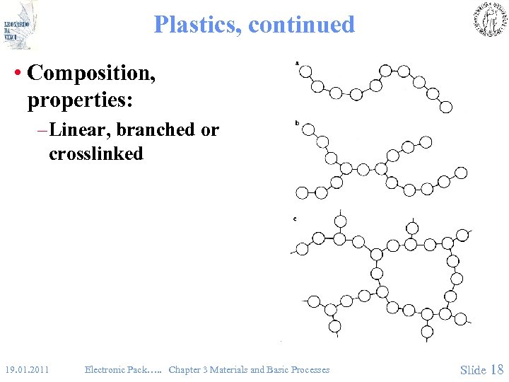
Plastics, continued • Composition, properties: – Linear, branched or crosslinked 19. 01. 2011 Electronic Pack…. . Chapter 3 Materials and Basic Processes Slide 18
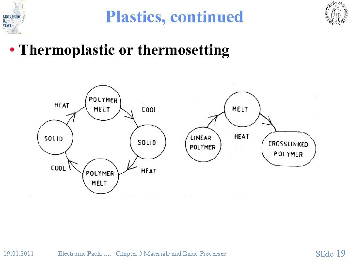
Plastics, continued • Thermoplastic or thermosetting 19. 01. 2011 Electronic Pack…. . Chapter 3 Materials and Basic Processes Slide 19
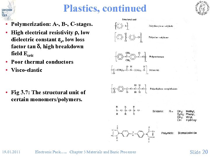
Plastics, continued • Polymerization: A-, B-, C-stages. • High electrical resistivity , low dielectric constant r, low loss factor tan , high breakdown field Ecrit • Poor thermal conductors • Visco-elastic • Fig 3. 7: The structural unit of certain monomers/polymers. 19. 01. 2011 Electronic Pack…. . Chapter 3 Materials and Basic Processes Slide 20
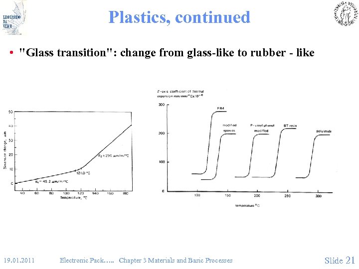
Plastics, continued • "Glass transition": change from glass-like to rubber - like 19. 01. 2011 Electronic Pack…. . Chapter 3 Materials and Basic Processes Slide 21
Plastic Materials: • • • Epoxy Phenolic Polyimide Teflon Polyester Silicone Polyurethane Parylene Acrylic Polysulphone, polyetherimide 19. 01. 2011 Electronic Pack…. . Chapter 3 Materials and Basic Processes Slide 22
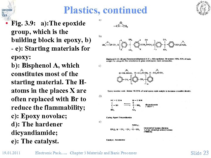
Plastics, continued • Fig. 3. 9: a): The epoxide group, which is the building block in epoxy, b) - e): Starting materials for epoxy: b): Bisphenol A, which constitutes most of the starting material. The Hatoms in the places X are often replaced with Br to reduce the flammability; c): Epoxy novolac; d): The hardener dicyandiamide; e): The catalyst. 19. 01. 2011 Electronic Pack…. . Chapter 3 Materials and Basic Processes Slide 23
Plastics, continued 19. 01. 2011 Electronic Pack…. . Chapter 3 Materials and Basic Processes Slide 24
Basic Processes • Description of some of the basic processes used in microelectronics, microsystems and electronic packaging. 19. 01. 2011 Electronic Pack…. . Chapter 3 Materials and Basic Processes Slide 25
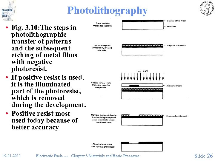
Photolithography • Fig. 3. 10: The steps in photolithographic transfer of patterns and the subsequent etching of metal films with negative photoresist. • If positive resist is used, it is the illuminated part of the photoresist, which is removed during the development. • Positive resist most used today because of better accuracy 19. 01. 2011 Electronic Pack…. . Chapter 3 Materials and Basic Processes Slide 26
Photolithography, cont • Also, please observe the concept of straight polarity masks and reverse polarity masks: – Straight polarity: In layers with straight polarity, a positive image of the layout will be transferred onto the process layer. In other words, draw the objects that need to be covered with photo-resist after development. • Openings: Mask pattern is repeated on the substrate for additive films etc. , like metal patterns. (Assuming positive resist is used) – Reverse polarity: In layers with reverse polarity, draw the areas where photoresist should be removed. The actual mask will be the negative image of the layout. • Mask pattern is oppositely repeated on the substrate for additive films etc. , like openings in oxide for later difussion of dopants. (Assuming positive resist is used) 19. 01. 2011 Electronic Pack…. . Chapter 3 Materials and Basic Processes Slide 27
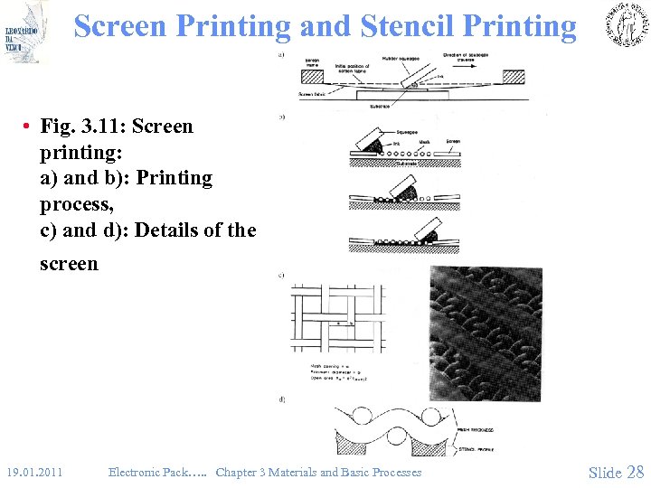
Screen Printing and Stencil Printing • Fig. 3. 11: Screen printing: a) and b): Printing process, c) and d): Details of the screen 19. 01. 2011 Electronic Pack…. . Chapter 3 Materials and Basic Processes Slide 28
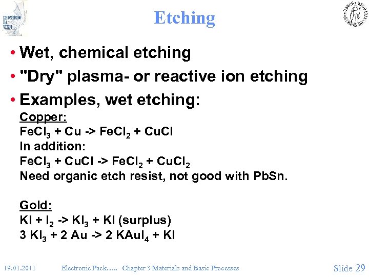
Etching • Wet, chemical etching • "Dry" plasma- or reactive ion etching • Examples, wet etching: Copper: Fe. Cl 3 + Cu -> Fe. Cl 2 + Cu. Cl In addition: Fe. Cl 3 + Cu. Cl -> Fe. Cl 2 + Cu. Cl 2 Need organic etch resist, not good with Pb. Sn. Gold: KI + I 2 -> KI 3 + KI (surplus) 3 KI 3 + 2 Au -> 2 KAu. I 4 + KI 19. 01. 2011 Electronic Pack…. . Chapter 3 Materials and Basic Processes Slide 29
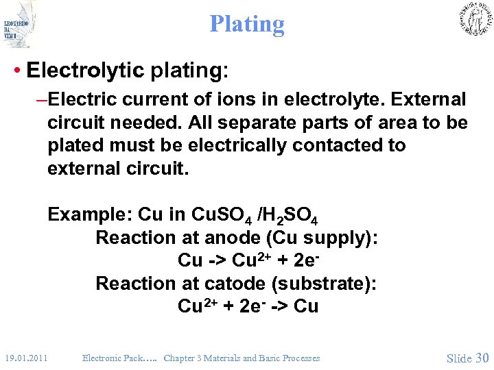
Plating • Electrolytic plating: –Electric current of ions in electrolyte. External circuit needed. All separate parts of area to be plated must be electrically contacted to external circuit. Example: Cu in Cu. SO 4 /H 2 SO 4 Reaction at anode (Cu supply): Cu -> Cu 2+ + 2 e. Reaction at catode (substrate): Cu 2+ + 2 e- -> Cu 19. 01. 2011 Electronic Pack…. . Chapter 3 Materials and Basic Processes Slide 30
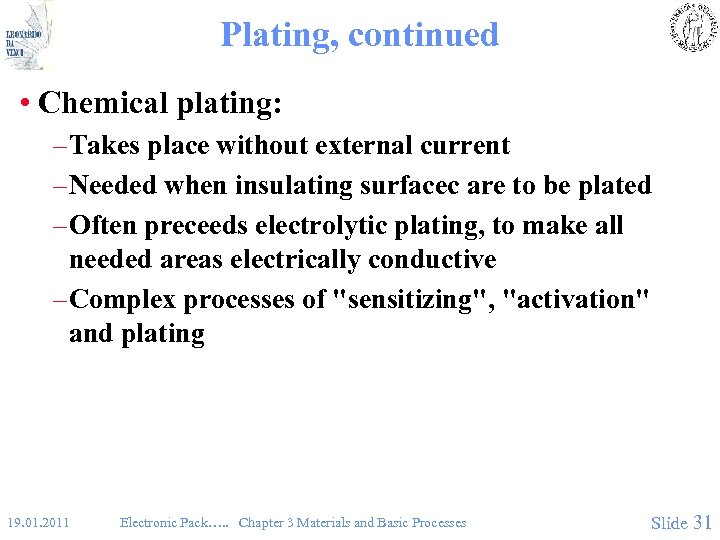
Plating, continued • Chemical plating: – Takes place without external current – Needed when insulating surfacec are to be plated – Often preceeds electrolytic plating, to make all needed areas electrically conductive – Complex processes of "sensitizing", "activation" and plating 19. 01. 2011 Electronic Pack…. . Chapter 3 Materials and Basic Processes Slide 31
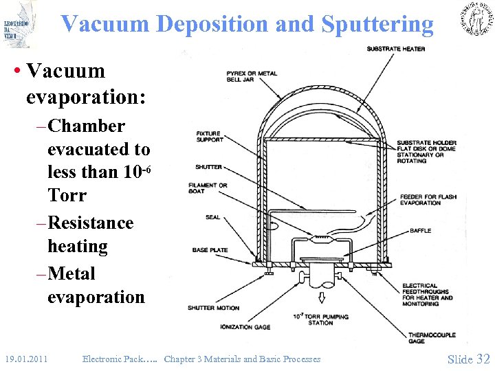
Vacuum Deposition and Sputtering • Vacuum evaporation: – Chamber evacuated to less than 10 -6 Torr – Resistance heating – Metal evaporation 19. 01. 2011 Electronic Pack…. . Chapter 3 Materials and Basic Processes Slide 32
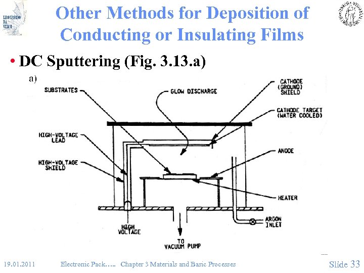
Other Methods for Deposition of Conducting or Insulating Films • DC Sputtering (Fig. 3. 13. a) 19. 01. 2011 Electronic Pack…. . Chapter 3 Materials and Basic Processes Slide 33
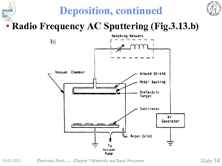
Deposition, continued • Radio Frequency AC Sputtering (Fig. 3. 13. b) 19. 01. 2011 Electronic Pack…. . Chapter 3 Materials and Basic Processes Slide 34
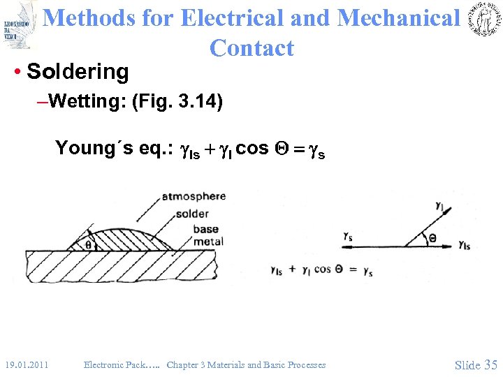
Methods for Electrical and Mechanical Contact • Soldering –Wetting: (Fig. 3. 14) Young´s eq. : gls + gl cos Q = gs 19. 01. 2011 Electronic Pack…. . Chapter 3 Materials and Basic Processes Slide 35
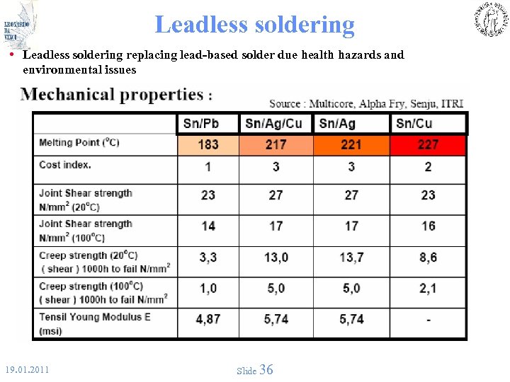
Leadless soldering • Leadless soldering replacing lead-based solder due health hazards and environmental issues 19. 01. 2011 Slide 36
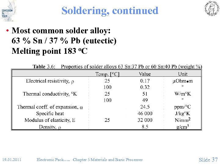
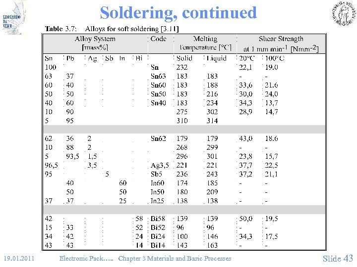
Soldering, continued • Most common solder alloy: 63 % Sn / 37 % Pb (eutectic) Melting point 183 o. C 19. 01. 2011 Electronic Pack…. . Chapter 3 Materials and Basic Processes Slide 37
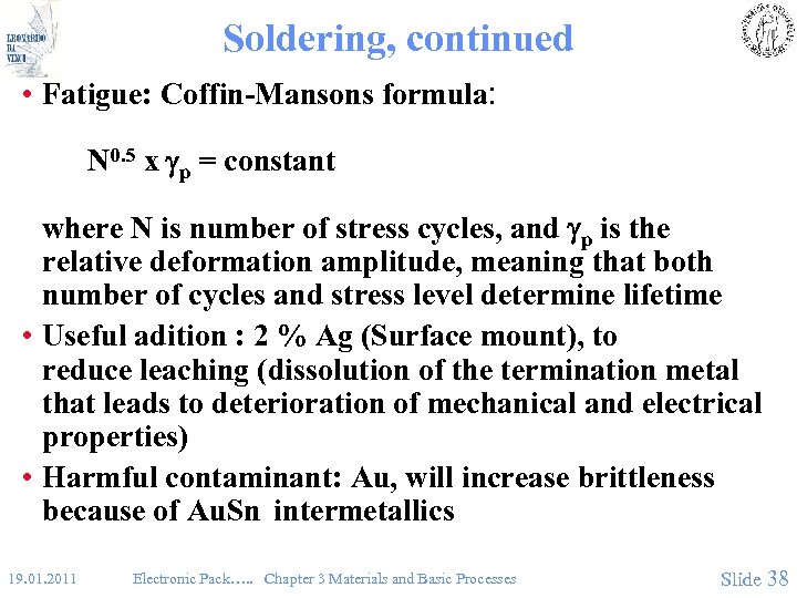
Soldering, continued • Fatigue: Coffin-Mansons formula: N 0. 5 x gp = constant where N is number of stress cycles, and gp is the relative deformation amplitude, meaning that both number of cycles and stress level determine lifetime • Useful adition : 2 % Ag (Surface mount), to reduce leaching (dissolution of the termination metal that leads to deterioration of mechanical and electrical properties) • Harmful contaminant: Au, will increase brittleness because of Au. Sn intermetallics 19. 01. 2011 Electronic Pack…. . Chapter 3 Materials and Basic Processes Slide 38
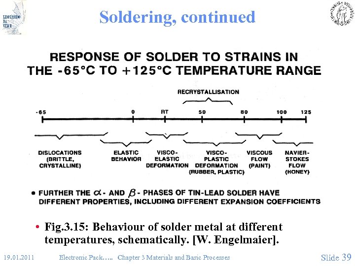
Soldering, continued • Fig. 3. 15: Behaviour of solder metal at different temperatures, schematically. [W. Engelmaier]. 19. 01. 2011 Electronic Pack…. . Chapter 3 Materials and Basic Processes Slide 39
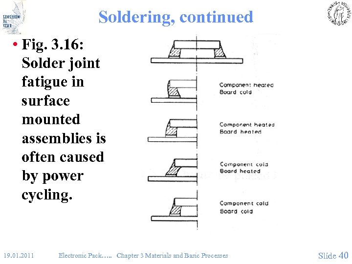
Soldering, continued • Fig. 3. 16: Solder joint fatigue in surface mounted assemblies is often caused by power cycling. 19. 01. 2011 Electronic Pack…. . Chapter 3 Materials and Basic Processes Slide 40
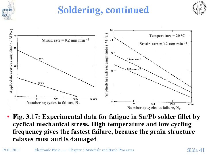
Soldering, continued • Fig. 3. 17: Experimental data for fatigue in Sn/Pb solder fillet by cyclical mechanical stress. High temperature and low cycling frequency gives the fastest failure, because the grain structure relaxes most and is damaged 19. 01. 2011 Electronic Pack…. . Chapter 3 Materials and Basic Processes Slide 41
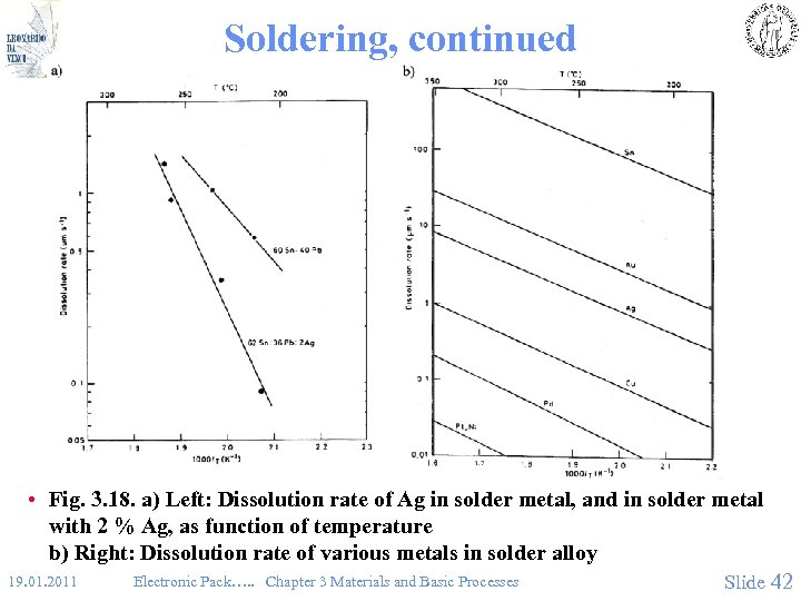
Soldering, continued • Fig. 3. 18. a) Left: Dissolution rate of Ag in solder metal, and in solder metal with 2 % Ag, as function of temperature b) Right: Dissolution rate of various metals in solder alloy 19. 01. 2011 Electronic Pack…. . Chapter 3 Materials and Basic Processes Slide 42
Soldering, continued 19. 01. 2011 Electronic Pack…. . Chapter 3 Materials and Basic Processes Slide 43
Soldering, continued • Flux and cleaning – Purpose of flux: • Dissolve and remove oxides etc. • Protect surface • Improve wetting – Categories: • Soluble in organic liquids • Water soluble – Types: • Organic resin fluxes ("rosin") • Organic non resin based fluxes • Inorganic fluxes 19. 01. 2011 Electronic Pack…. . Chapter 3 Materials and Basic Processes Slide 44
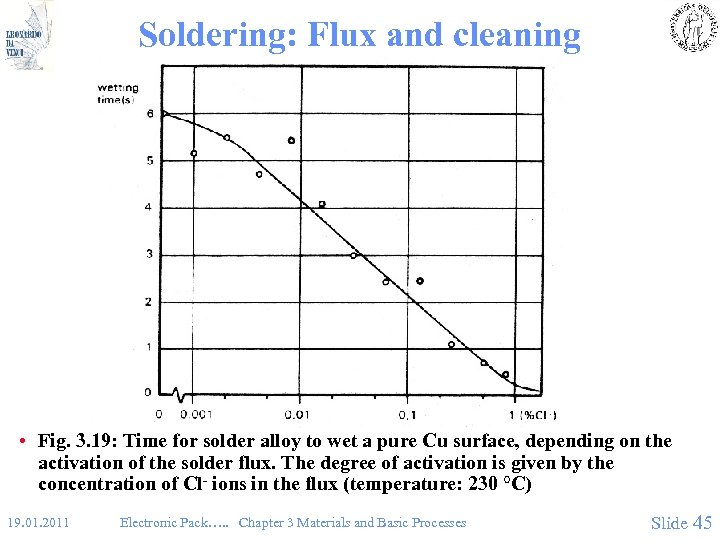
Soldering: Flux and cleaning • Fig. 3. 19: Time for solder alloy to wet a pure Cu surface, depending on the activation of the solder flux. The degree of activation is given by the concentration of Cl- ions in the flux (temperature: 230 °C) 19. 01. 2011 Electronic Pack…. . Chapter 3 Materials and Basic Processes Slide 45
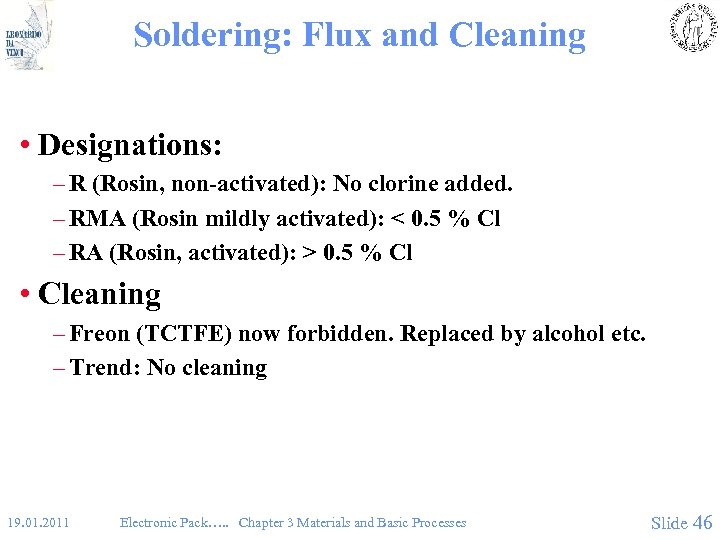
Soldering: Flux and Cleaning • Designations: – R (Rosin, non-activated): No clorine added. – RMA (Rosin mildly activated): < 0. 5 % Cl – RA (Rosin, activated): > 0. 5 % Cl • Cleaning – Freon (TCTFE) now forbidden. Replaced by alcohol etc. – Trend: No cleaning 19. 01. 2011 Electronic Pack…. . Chapter 3 Materials and Basic Processes Slide 46
Gluing • Purposes: – Mechanical assembly – Electrical contact – Thermal contact • Materials: polymers: – Epoxy, acrylic, phenolic, polyimide – Metal particles for electrical conductivity: r = 1 - 10 x 10 -6 ohm m – Metal or ceramic particles for thermal conductivity: K ≈ 1 - 3 W /m x o. C 19. 01. 2011 Electronic Pack…. . Chapter 3 Materials and Basic Processes Slide 47
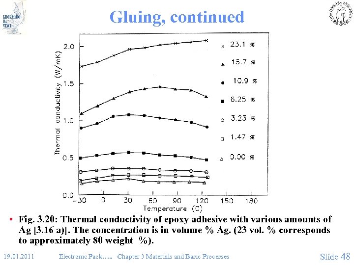
Gluing, continued • Fig. 3. 20: Thermal conductivity of epoxy adhesive with various amounts of Ag [3. 16 a)]. The concentration is in volume % Ag. (23 vol. % corresponds to approximately 80 weight %). 19. 01. 2011 Electronic Pack…. . Chapter 3 Materials and Basic Processes Slide 48
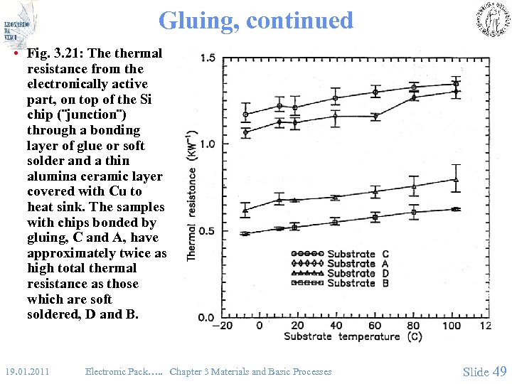
Gluing, continued • Fig. 3. 21: The thermal resistance from the electronically active part, on top of the Si chip (¨junction¨) through a bonding layer of glue or soft solder and a thin alumina ceramic layer covered with Cu to heat sink. The samples with chips bonded by gluing, C and A, have approximately twice as high total thermal resistance as those which are soft soldered, D and B. 19. 01. 2011 Electronic Pack…. . Chapter 3 Materials and Basic Processes Slide 49
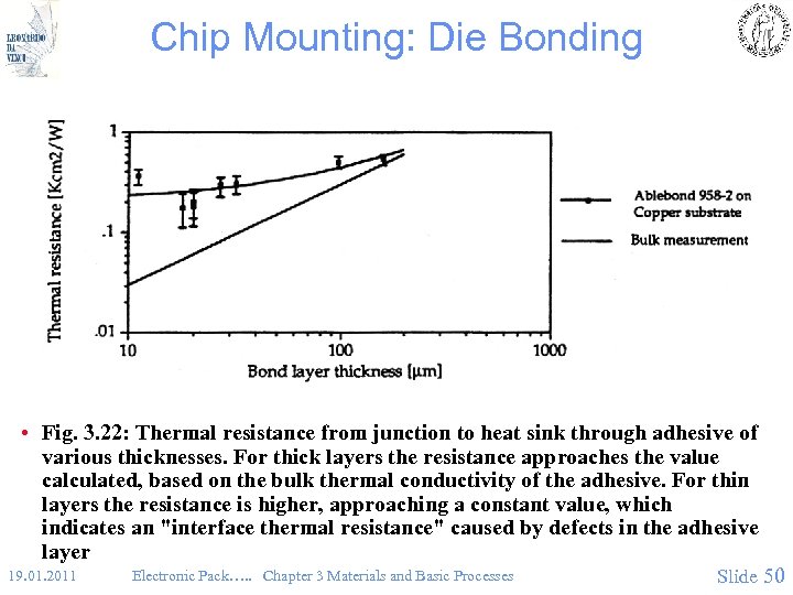
Chip Mounting: Die Bonding • Fig. 3. 22: Thermal resistance from junction to heat sink through adhesive of various thicknesses. For thick layers the resistance approaches the value calculated, based on the bulk thermal conductivity of the adhesive. For thin layers the resistance is higher, approaching a constant value, which indicates an "interface thermal resistance" caused by defects in the adhesive layer 19. 01. 2011 Electronic Pack…. . Chapter 3 Materials and Basic Processes Slide 50
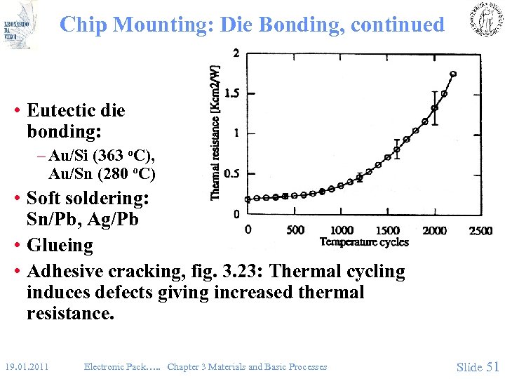
Chip Mounting: Die Bonding, continued • Eutectic die bonding: – Au/Si (363 o. C), Au/Sn (280 o. C) • Soft soldering: Sn/Pb, Ag/Pb • Glueing • Adhesive cracking, fig. 3. 23: Thermal cycling induces defects giving increased thermal resistance. 19. 01. 2011 Electronic Pack…. . Chapter 3 Materials and Basic Processes Slide 51
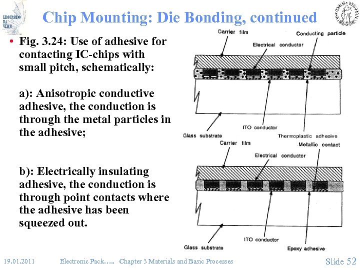
Chip Mounting: Die Bonding, continued • Fig. 3. 24: Use of adhesive for contacting IC-chips with small pitch, schematically: a): Anisotropic conductive adhesive, the conduction is through the metal particles in the adhesive; b): Electrically insulating adhesive, the conduction is through point contacts where the adhesive has been squeezed out. 19. 01. 2011 Electronic Pack…. . Chapter 3 Materials and Basic Processes Slide 52
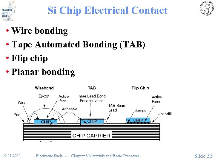
Si Chip Electrical Contact • Wire bonding • Tape Automated Bonding (TAB) • Flip chip • Planar bonding 19. 01. 2011 Electronic Pack…. . Chapter 3 Materials and Basic Processes Slide 53
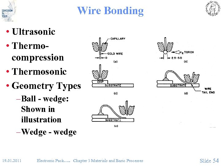
Wire Bonding • Ultrasonic • Thermocompression • Thermosonic • Geometry Types – Ball - wedge: Shown in illustration – Wedge - wedge 19. 01. 2011 Electronic Pack…. . Chapter 3 Materials and Basic Processes Slide 54
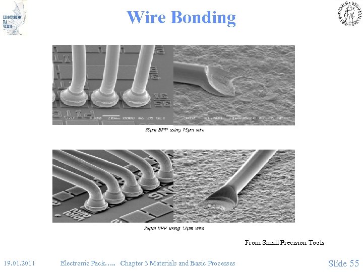
Wire Bonding From Small Precision Tools 19. 01. 2011 Electronic Pack…. . Chapter 3 Materials and Basic Processes Slide 55
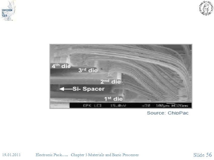
19. 01. 2011 Electronic Pack…. . Chapter 3 Materials and Basic Processes Slide 56
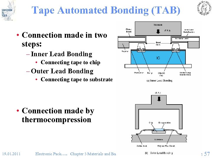
Tape Automated Bonding (TAB) • Connection made in two steps: – Inner Lead Bonding • Connecting tape to chip – Outer Lead Bonding • Connecting tape to substrate • Connection made by thermocompression 19. 01. 2011 Electronic Pack…. . Chapter 3 Materials and Basic Processes Slide 57
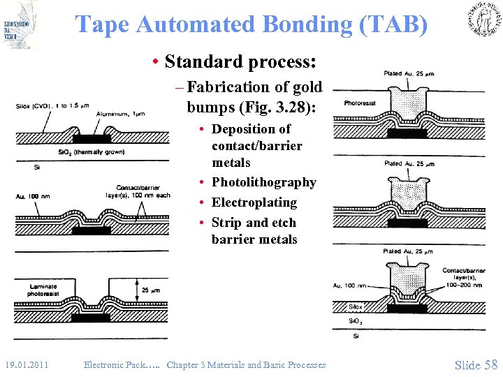
Tape Automated Bonding (TAB) • Standard process: – Fabrication of gold bumps (Fig. 3. 28): • Deposition of contact/barrier metals • Photolithography • Electroplating • Strip and etch barrier metals 19. 01. 2011 Electronic Pack…. . Chapter 3 Materials and Basic Processes Slide 58
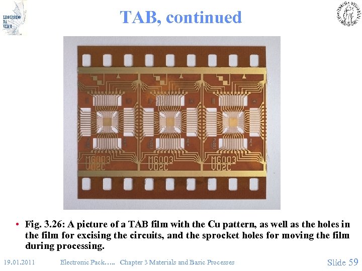
TAB, continued • Fig. 3. 26: A picture of a TAB film with the Cu pattern, as well as the holes in the film for excising the circuits, and the sprocket holes for moving the film during processing. 19. 01. 2011 Electronic Pack…. . Chapter 3 Materials and Basic Processes Slide 59
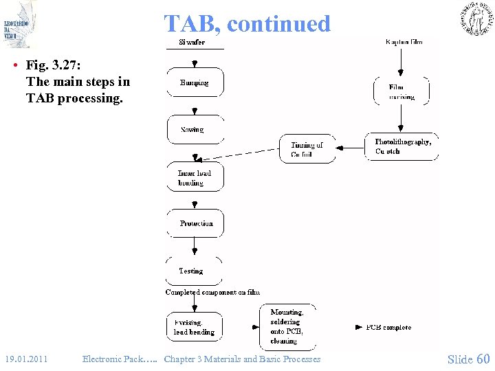
TAB, continued • Fig. 3. 27: The main steps in TAB processing. 19. 01. 2011 Electronic Pack…. . Chapter 3 Materials and Basic Processes Slide 60
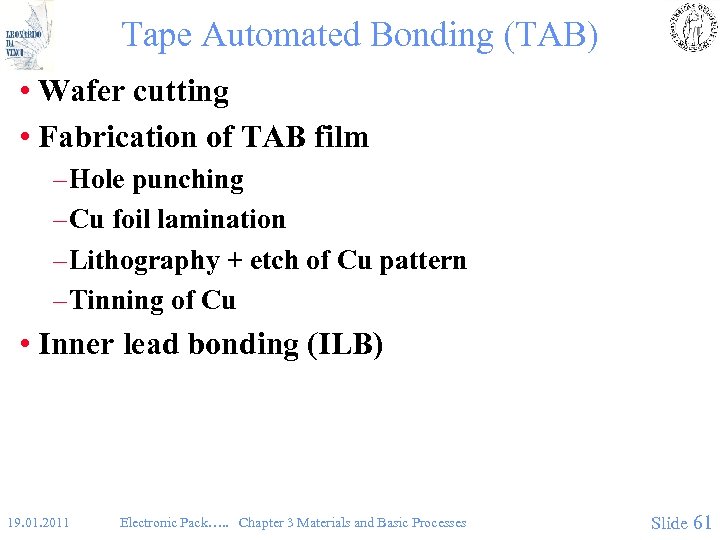
Tape Automated Bonding (TAB) • Wafer cutting • Fabrication of TAB film – Hole punching – Cu foil lamination – Lithography + etch of Cu pattern – Tinning of Cu • Inner lead bonding (ILB) 19. 01. 2011 Electronic Pack…. . Chapter 3 Materials and Basic Processes Slide 61
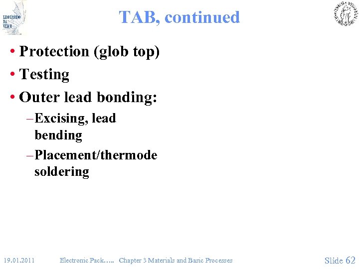
TAB, continued • Protection (glob top) • Testing • Outer lead bonding: – Excising, lead bending – Placement/thermode soldering 19. 01. 2011 Electronic Pack…. . Chapter 3 Materials and Basic Processes Slide 62
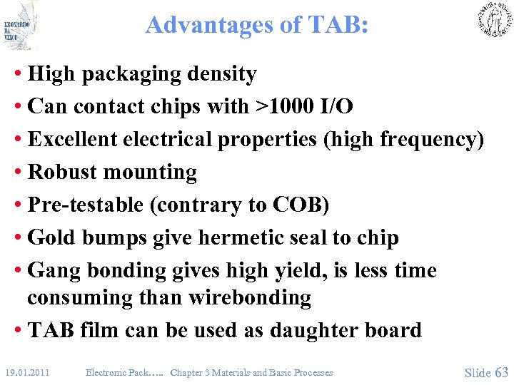
Advantages of TAB: • High packaging density • Can contact chips with >1000 I/O • Excellent electrical properties (high frequency) • Robust mounting • Pre-testable (contrary to COB) • Gold bumps give hermetic seal to chip • Gang bonding gives high yield, is less time consuming than wirebonding • TAB film can be used as daughter board 19. 01. 2011 Electronic Pack…. . Chapter 3 Materials and Basic Processes Slide 63
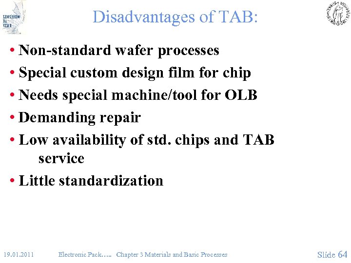
Disadvantages of TAB: • Non-standard wafer processes • Special custom design film for chip • Needs special machine/tool for OLB • Demanding repair • Low availability of std. chips and TAB service • Little standardization 19. 01. 2011 Electronic Pack…. . Chapter 3 Materials and Basic Processes Slide 64
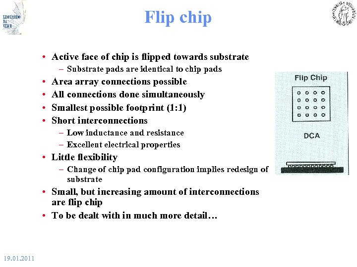
Flip chip • Active face of chip is flipped towards substrate – Substrate pads are identical to chip pads • • Area array connections possible All connections done simultaneously Smallest possible footprint (1: 1) Short interconnections – Low inductance and resistance – Excellent electrical properties • Little flexibility – Change of chip pad configuration implies redesign of substrate • Small, but increasing amount of interconnections are flip chip • To be dealt with in much more detail… 19. 01. 2011
Flip Chip • Process: – Deposit barrier metals – Deposit solder bump metals (solder) by photolithography/metal mask and sputter or plating – Reflow – Cut wafer – Turn chip and mount on substrate – Heat substrate to reflow solder 19. 01. 2011 Electronic Pack…. . Chapter 3 Materials and Basic Processes Slide 66
Flip Chip, history • Introduced by IBM 1962 • Flip chip has been used for decades, but with little impact – Wire bonding is far more common – Flip chip technology has not been considered mature – The industrial infrastructure has been small • The market share of flip chip connections is believed to increase significantly – Wire bonding will remain dominating for many years • Flip chip especially for ”advanced packaging” 19. 01. 2011
Flip Chip, continued • Advantages: – Highest packing density – Excellent hi freq. properties – Up to 10 000 I/O • Disadvantages: – Very difficult placement and reliable solder/cleaning – Lack of thermal flexibility 19. 01. 2011 Electronic Pack…. . Chapter 3 Materials and Basic Processes Slide 68
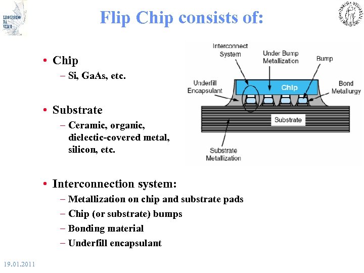
Flip Chip consists of: • Chip – Si, Ga. As, etc. • Substrate – Ceramic, organic, dielectic-covered metal, silicon, etc. • Interconnection system: – Metallization on chip and substrate pads – Chip (or substrate) bumps – Bonding material – Underfill encapsulant 19. 01. 2011
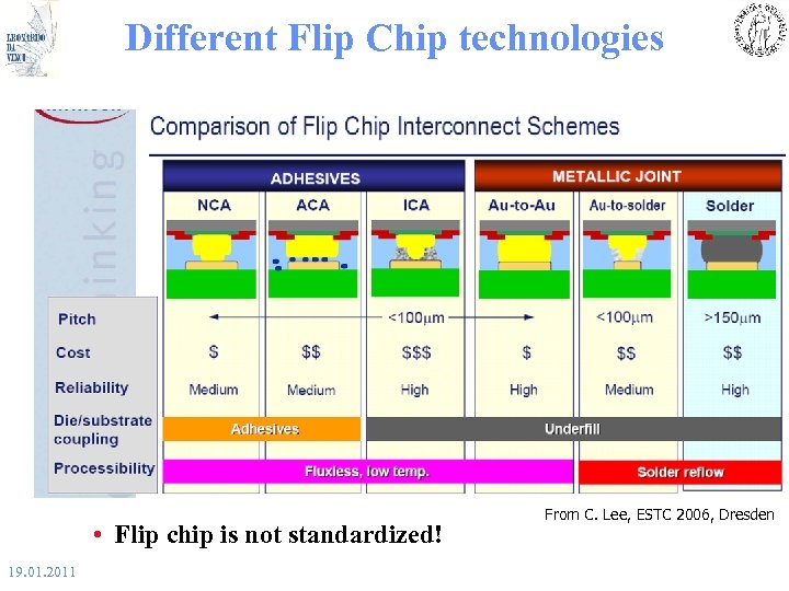
Different Flip Chip technologies • Flip chip is not standardized! 19. 01. 2011 From C. Lee, ESTC 2006, Dresden
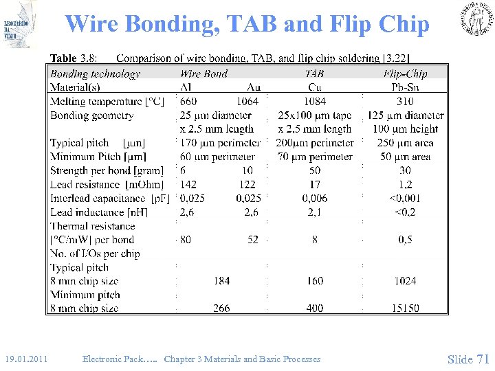
Wire Bonding, TAB and Flip Chip 19. 01. 2011 Electronic Pack…. . Chapter 3 Materials and Basic Processes Slide 71
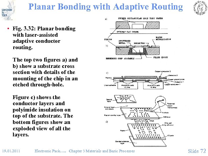
Planar Bonding with Adaptive Routing • Fig. 3. 32: Planar bonding with laser-assisted adaptive conductor routing. The top two figures a) and b) show a substrate cross section with details of the mounting of the chip in an etched through-hole. Figure c) shows the conductor layers and polyimide insulation on top of the substrate. The bottom figures show an exploded view of all the layers. 19. 01. 2011 Electronic Pack…. . Chapter 3 Materials and Basic Processes Slide 72
End of Chapter 3 Materials and Basic Processes • Important issues: – Materials: • Distinguish between metals, ceramics, glasses and plastics – Important mechanical and thermal parameters like modulus of eleasticity, thermal expansion coefficient and thermal conductivity. – Important electrical parameters like dielectric constant and resistivity or conductivity – Have a basic understand of the importance and value of the most important materials parameter, and why they are important for the use of the specific material in specific applications. – For instance knowing the electrical conductivity of copper or thermal conductivity of epoxy within an accuracy of 25% – Basic processes • Lithographics, screen and stencil printing, etching, plating, vacuum deposition, sputtering, soldering, gluing, wire bonding, TAB, and flip chip – Other basic processes described in other chapters, like surface mount technology • Questions and discussions? 19. 01. 2011 Electronic Pack…. . Chapter 3 Materials and Basic Processes Slide 73
a8e700fd07db557a725867742ce9ef57.ppt