88917afdd7553827e3bc6ae7ce119fa3.ppt
- Количество слайдов: 60
 Chapter 3 – Diodes Introduction http: //jas 2. eng. buffalo. edu/applets/education/pn/biased. PN/index. html http: //jas 2. eng. buffalo. edu/applets/education/pn/cv/index. html Textbook CD
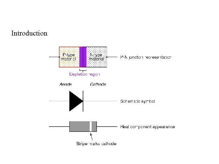 Introduction
 The Ideal Diode The ideal diode: (a) diode circuit symbol; (b) i-v characteristic; (c) equivalent circuit in the reverse direction; (d) equivalent circuit in the forward direction.
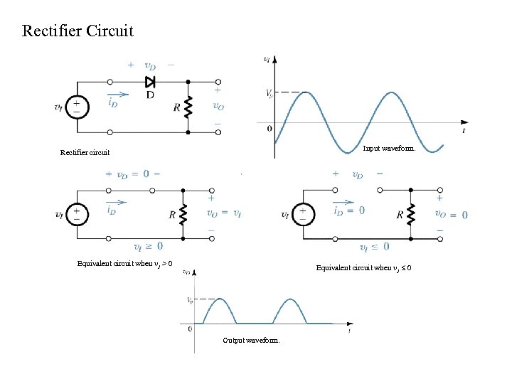 Rectifier Circuit Input waveform. Rectifier circuit Equivalent circuit when v 1 > 0 Equivalent circuit when v 1 0 Output waveform.
 Rectifier Circuit Example 3. 1
 Rectifier Circuit Example 3. 2
 Terminal Characteristics of Junction Diodes – Forward Region Example 3. 3
 Terminal Characteristics of Junction Diodes – Reverse-Bias Region Exercise 3. 9
 Rectifier Circuit Exercises 3. 4 and 3. 5
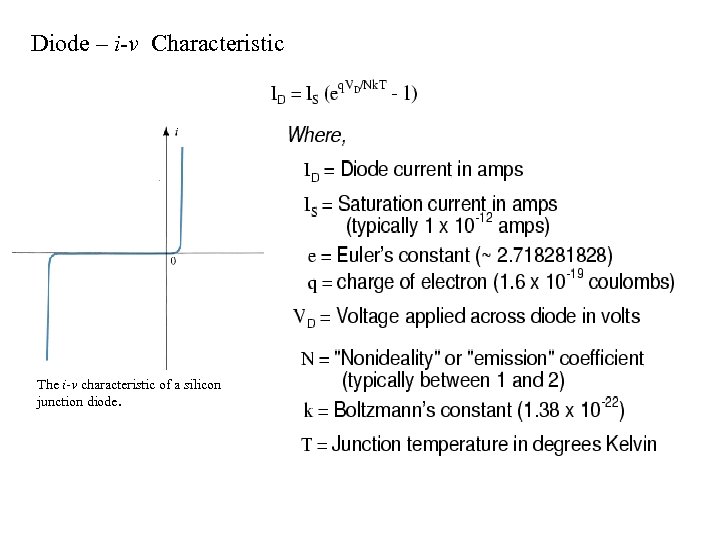 Diode – i-v Characteristic The i-v characteristic of a silicon junction diode.
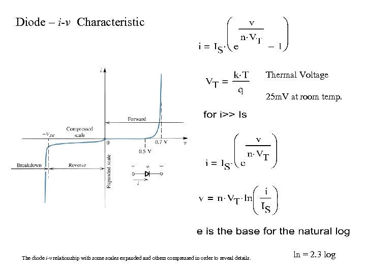 Diode – i-v Characteristic Thermal Voltage 25 m. V at room temp. The diode i-v relationship with some scales expanded and others compressed in order to reveal details. ln = 2. 3 log
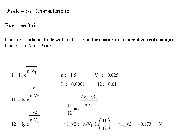 Diode – i-v Characteristic Exercise 3. 6 Consider a silicon diode with n=1. 5. Find the change in voltage if current changes from 0. 1 m. A to 10 m. A.
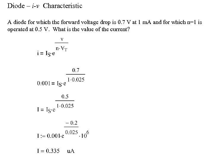 Diode – i-v Characteristic A diode for which the forward voltage drop is 0. 7 V at 1 m. A and for which n=1 is operated at 0. 5 V. What is the value of the current?
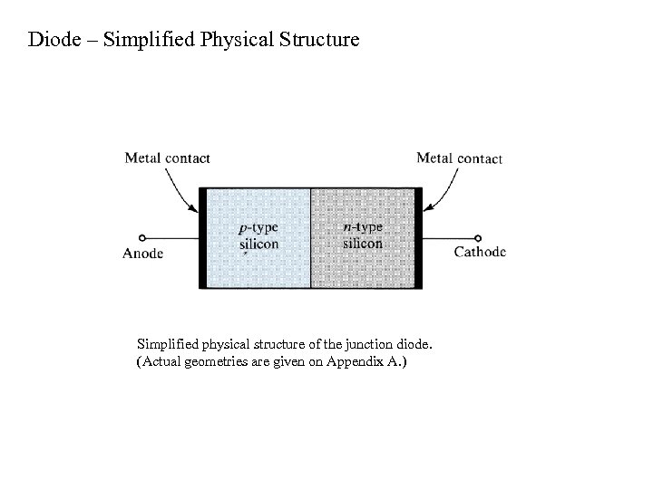 Diode – Simplified Physical Structure Simplified physical structure of the junction diode. (Actual geometries are given on Appendix A. )
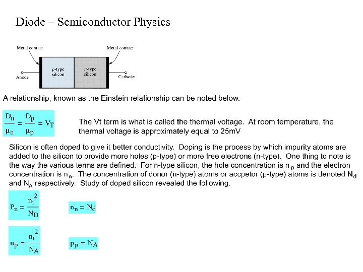
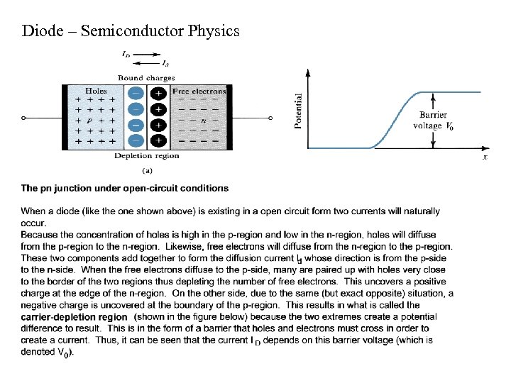
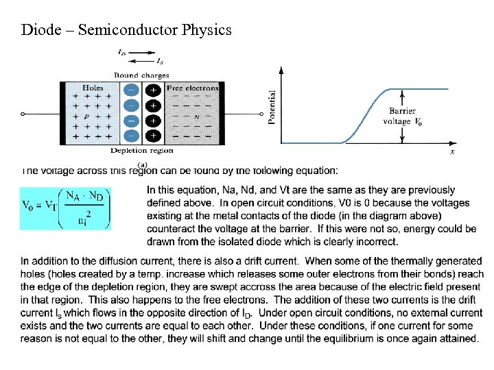
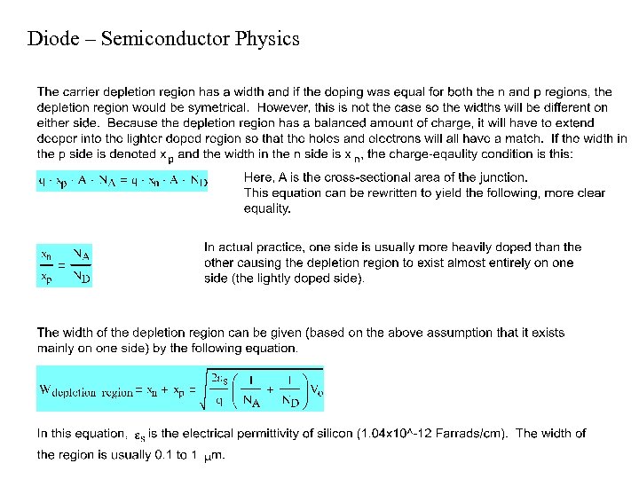
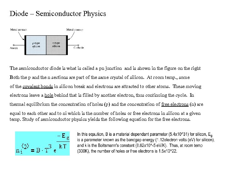 Diode – Semiconductor Physics The semiconductor diode is what is called a pn junction and is shown in the figure on the right Both the p and the n sections are part of the same crystal of silicon. At room temp. , some of the covalent bonds in silicon break and electrons are attracted to other atoms. These moving electrons leave a hole behind that is filled by another electron, thus continuing the cycle. In thermal equilibrium the concentration of holes (p) and the concentration of free electrons (n) are equal to each other and to ni which is the number of holes or free electrons in silicon at a given temp. Study of semiconductor physics yields the following equation for the free electrons.
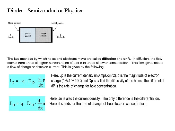 Diode – Semiconductor Physics
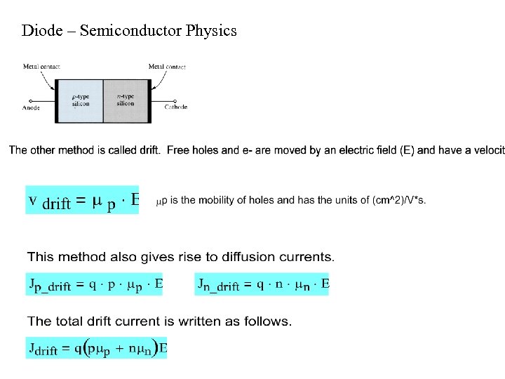 Diode – Semiconductor Physics
 Diode – Semiconductor Physics
 Diode – Semiconductor Physics
 Diode – Semiconductor Physics
 Diode – Semiconductor Physics
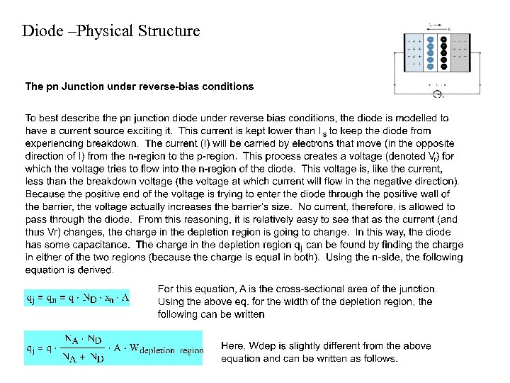 Diode –Physical Structure
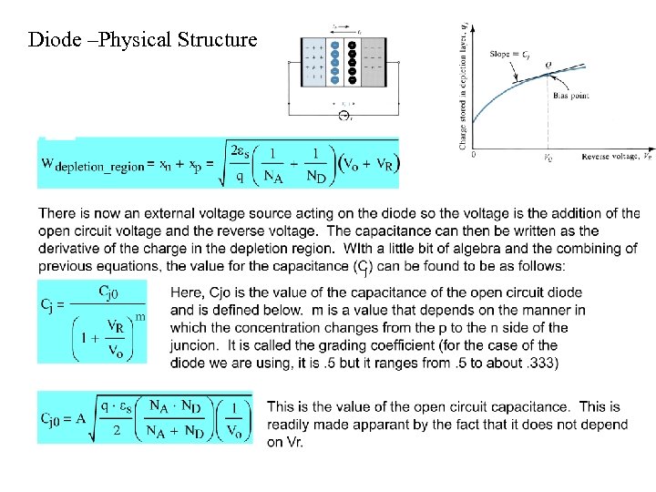 Diode –Physical Structure
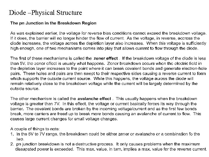 Diode –Physical Structure
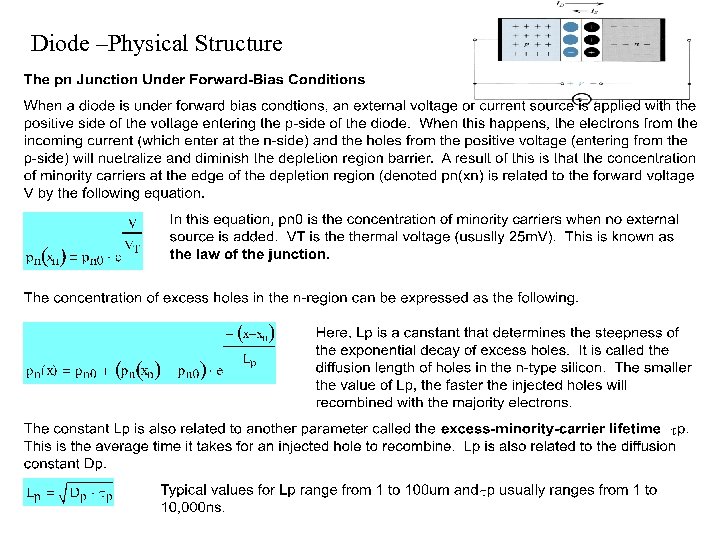 Diode –Physical Structure
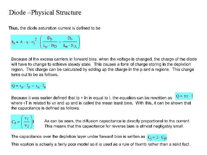
 Diode –Physical Structure Minority-carrier distribution in a forward-biased pn junction. It is assumed that the p region is more heavily doped than the n region; NA ND.
 Diode –Physical Structure
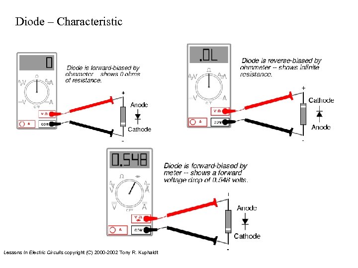 Diode – Characteristic Lessons In Electric Circuits copyright (C) 2000 -2002 Tony R. Kuphaldt
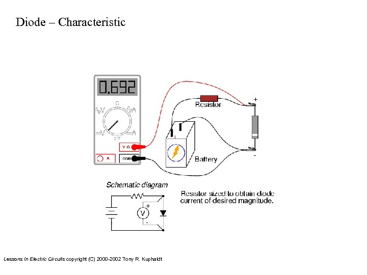 Diode – Characteristic Lessons In Electric Circuits copyright (C) 2000 -2002 Tony R. Kuphaldt
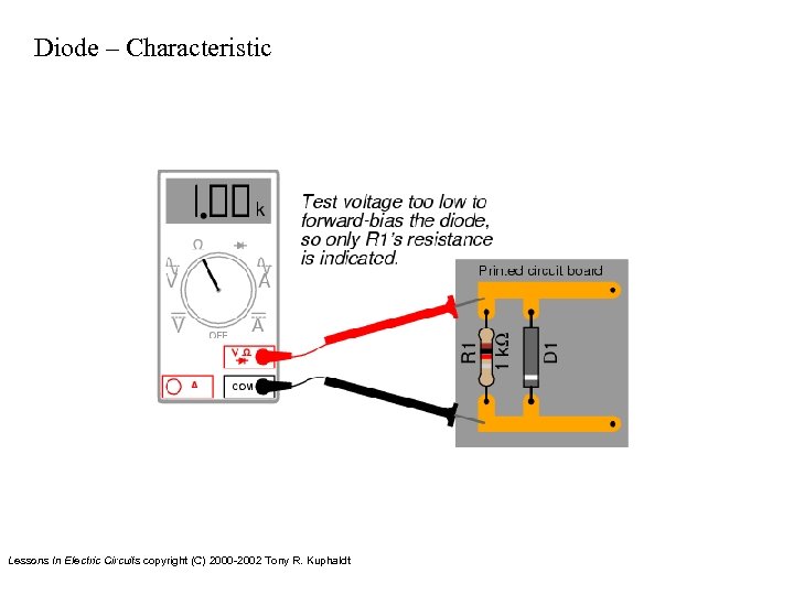 Diode – Characteristic Lessons In Electric Circuits copyright (C) 2000 -2002 Tony R. Kuphaldt
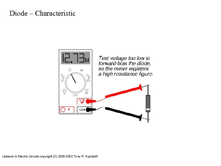 Diode – Characteristic Lessons In Electric Circuits copyright (C) 2000 -2002 Tony R. Kuphaldt
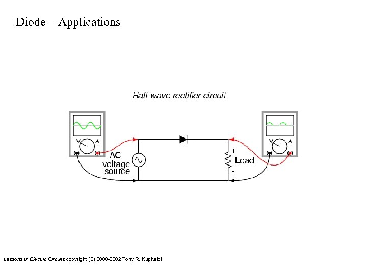 Diode – Applications Lessons In Electric Circuits copyright (C) 2000 -2002 Tony R. Kuphaldt
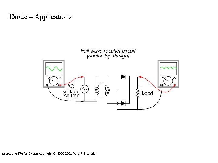 Diode – Applications Lessons In Electric Circuits copyright (C) 2000 -2002 Tony R. Kuphaldt
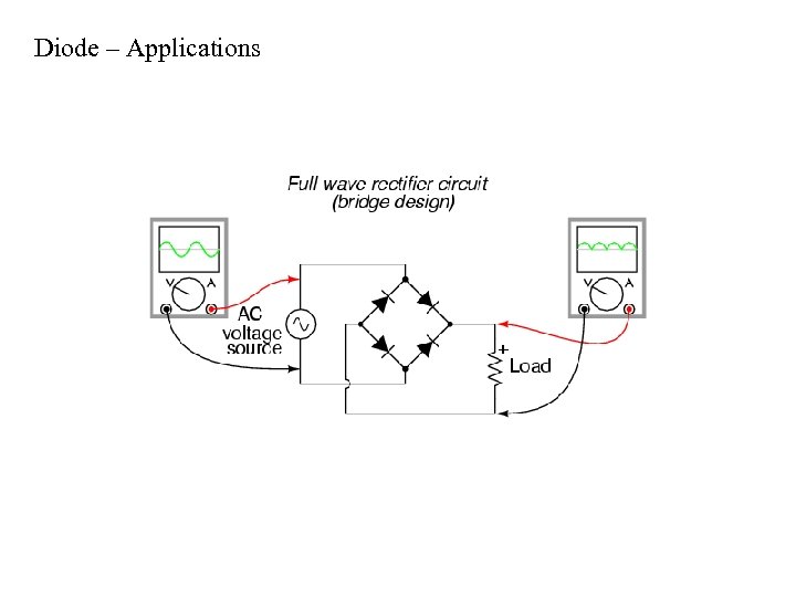 Diode – Applications
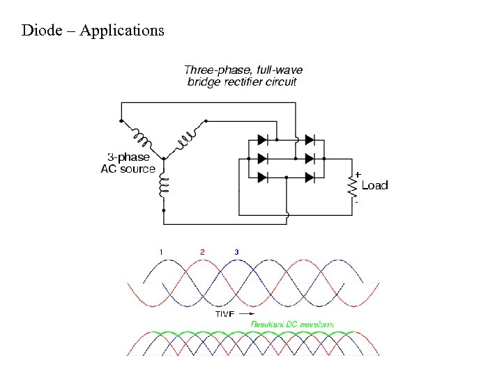 Diode – Applications
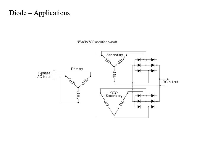 Diode – Applications
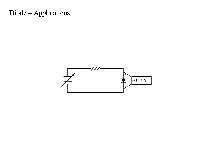 Diode – Applications
 Analysis of Diode Circuits A simple diode circuit.
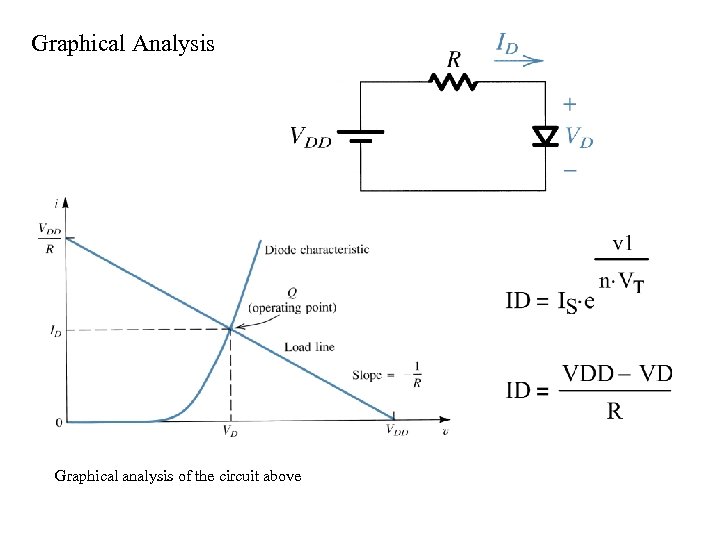 Graphical Analysis Graphical analysis of the circuit above
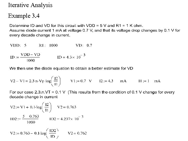 Iterative Analysis Example 3. 4
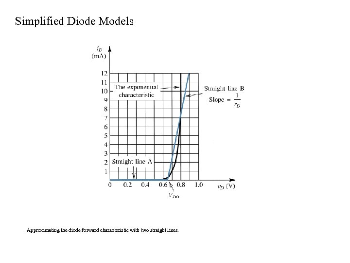 Simplified Diode Models Approximating the diode forward characteristic with two straight lines.
 Simplified Diode Models Example 3. 5 Piecewise-linear model of the diode forward characteristic and its equivalent circuit representation.
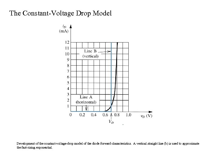 The Constant-Voltage Drop Model Development of the constant-voltage-drop model of the diode forward characteristics. A vertical straight line (b) is used to approximate the fast-rising exponential.
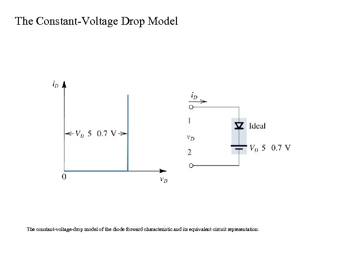 The Constant-Voltage Drop Model The constant-voltage-drop model of the diode forward characteristic and its equivalent circuit representation.
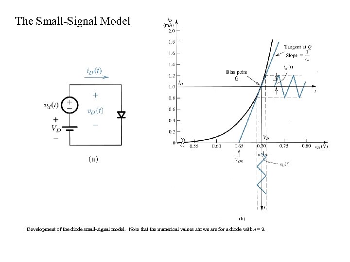 The Small-Signal Model Development of the diode small-signal model. Note that the numerical values shown are for a diode with n = 2.
 The Small-Signal Model Example 3. 6 Equivalent circuit model for the diode for small changes around bias point Q. The incremental resistance rd is the inverse of the slope of the tangent at Q, and VD 0 is the intercept of the tangent on the v. D axis.
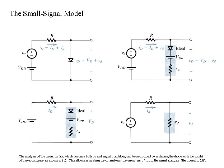 The Small-Signal Model The analysis of the circuit in (a), which contains both dc and signal quantities, can be performed by replacing the diode with the model of previous figure, as shown in (b). This allows separating the dc analysis [the circuit in (c)] from the signal analysis [the circuit in (d)].
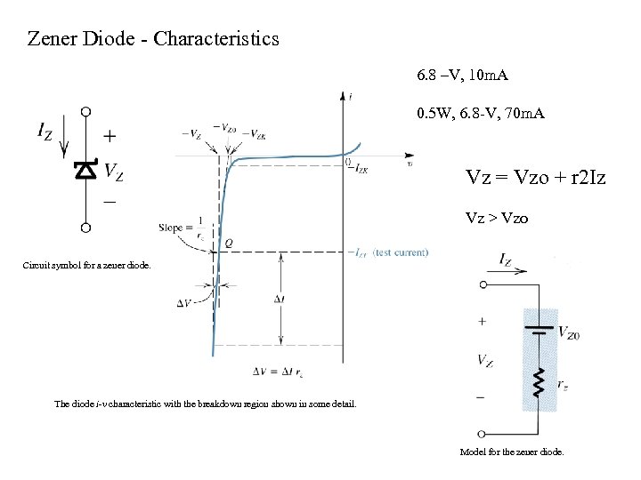 Zener Diode - Characteristics 6. 8 –V, 10 m. A 0. 5 W, 6. 8 -V, 70 m. A Vz = Vzo + r 2 Iz Vz > Vzo Circuit symbol for a zener diode. The diode i-v characteristic with the breakdown region shown in some detail. Model for the zener diode.
 Rectifier Circuits Block diagram of a dc power supply.
 Rectifier Circuits (a) Half-wave rectifier. (b) Equivalent circuit of the half-wave rectifier with the diode replaced with its battery-plusresistance model. (c) transfer characteristic of the rectifier circuit. (d) Input and output waveforms, assuming that r. D R.
 Rectifier Circuits Full-wave rectifier utilizing a transformer with a center-tapped secondary winding. (a) Circuit. (b) Transfer characteristic assuming a constant-voltage-drop model for the diodes. (c) Input and output waveforms.
 Rectifier Circuits The bridge rectifier: (a) circuit and (b) input and output waveforms. PIV Vs - VDO
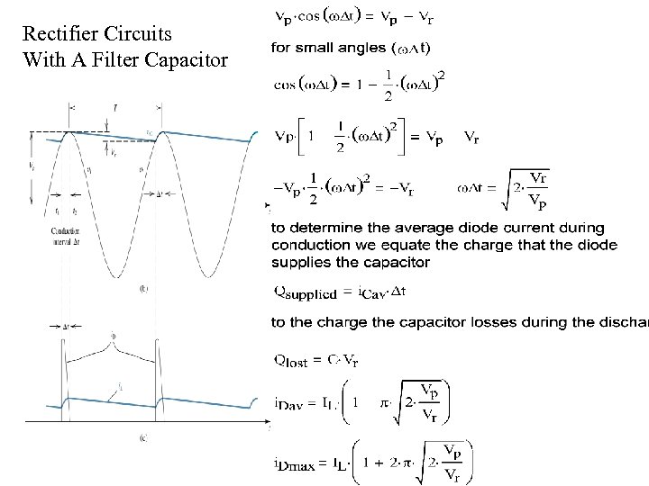
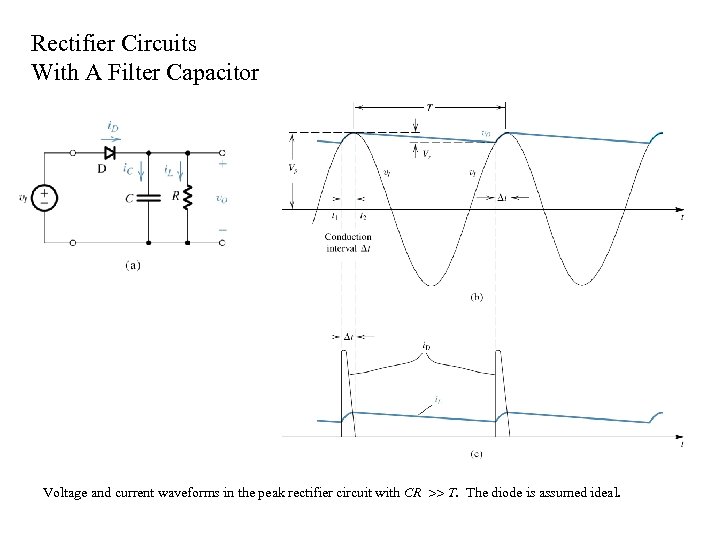 Rectifier Circuits With A Filter Capacitor Voltage and current waveforms in the peak rectifier circuit with CR T. The diode is assumed ideal.
 Rectifier Circuits With A Filter Capacitor
 Rectifier Circuits With A Filter Capacitor
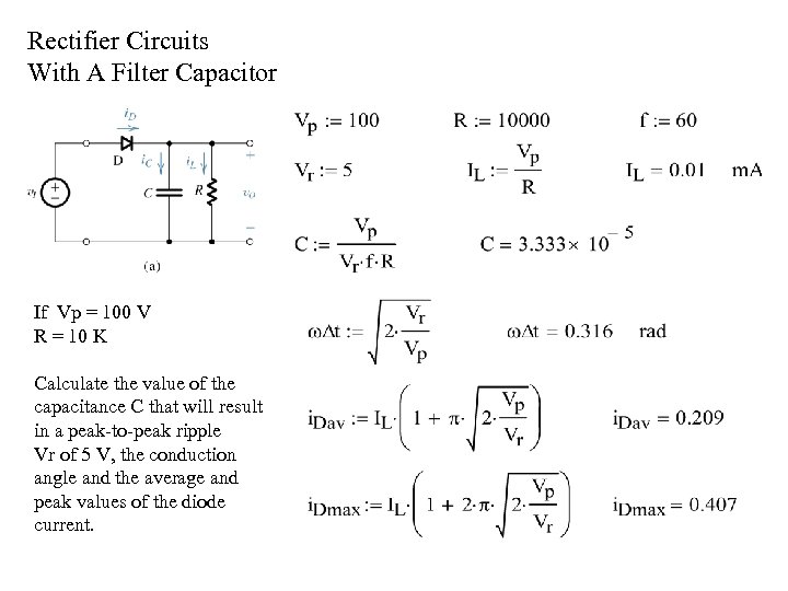 Rectifier Circuits With A Filter Capacitor If Vp = 100 V R = 10 K Calculate the value of the capacitance C that will result in a peak-to-peak ripple Vr of 5 V, the conduction angle and the average and peak values of the diode current.
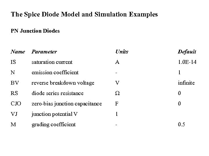
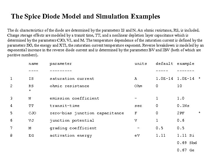 The Spice Diode Model and Simulation Examples The dc characteristics of the diode are determined by the parameters IS and N. An ohmic resistance, RS, is included. Charge storage effects are modeled by a transit time, TT, and a nonlinear depletion layer capacitance which is determined by the parameters CJO, VJ, and M. The temperature dependence of the saturation current is defined by the parameters EG, the energy and XTI, the saturation current temperature exponent. Reverse breakdown is modeled by an exponential increase in the reverse diode current and is determined by the parameters BV and IBV (both of which are positive numbers). name parameter units default example --------- 1 IS saturation current A 1. 0 E-14 * 2 RS * ohmic resistance Ohm 0 10 3 N emission coefficient - 1 1. 0 4 TT transit-time sec 0 0. 1 Ns 5 CJO zero-bias junction capacitance F 0 2 PF 6 VJ junction potential V 1 0. 6 7 M grading coefficient - 0. 5 8 EG activation energy e. V 1. 11 Si ------- 0. 69 Sbd 0. 67 Ge *
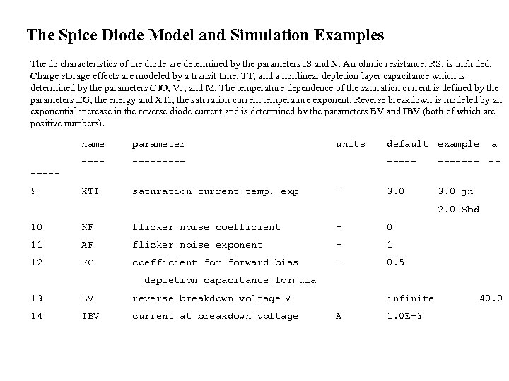 The Spice Diode Model and Simulation Examples The dc characteristics of the diode are determined by the parameters IS and N. An ohmic resistance, RS, is included. Charge storage effects are modeled by a transit time, TT, and a nonlinear depletion layer capacitance which is determined by the parameters CJO, VJ, and M. The temperature dependence of the saturation current is defined by the parameters EG, the energy and XTI, the saturation current temperature exponent. Reverse breakdown is modeled by an exponential increase in the reverse diode current and is determined by the parameters BV and IBV (both of which are positive numbers). name parameter --------- XTI saturation-current temp. exp units default example a ------- -- 3. 0 jn ----9 - 2. 0 Sbd 10 KF flicker noise coefficient - 0 11 AF flicker noise exponent - 1 12 FC coefficient forward-bias - 0. 5 depletion capacitance formula 13 BV reverse breakdown voltage V 14 IBV current at breakdown voltage infinite A 1. 0 E-3 40. 0
 The Spice Diode Model and Simulation Examples PN Junction Diodes Name Parameter Units Default IS saturation current A 1. 0 E-14 N emission coefficient - 1 BV reverse breakdown voltage V infinite RS diode series resistance 0 CJO zero-bias junction capacitance F 0 VJ junction potential V 1 M grading coefficient - 0. 5
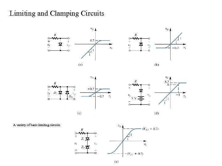 Limiting and Clamping Circuits A variety of basic limiting circuits.


