551c6877910bf6163130b7115879e1df.ppt
- Количество слайдов: 173
Chapter 11 Basic I/O Interface Ch. 11 Basic I/O Interface
Introduction µ : is great at solving problems but if can’t communicate with outside, it is of little worth outline some of basic methods of communications : both serial & parallel, between humans or machines and µ 1. introduce basic I/O interface, discuss decoding for I/O devices 2. provide detail on parallel and serial interfacing, both of which have a variety of applications 3. connect analog-to-digital and digital-to-analog converters, as well as both DC and stepper motors to µ Ch. 11 Basic I/O Interface 2
11 -1 Introduction to I/O interface explain : 1. operation of I/O instruction(IN, INS, OUTS) 2. concept of isolated(direct or I/O mapped I/O) and memory-mapped I/O 3. basic input and output interface 4. handshaking I/O instructions : Table 11 -1 IN, OUT : transfer data between I/O device and µ’s accumulator(AL, AX, EAX) variable address : 16 -bit I/O address in DX fixed address: 8 -bit form(p 8) immediately following opcode I/O address : port, port no, port address Ch. 11 Basic I/O Interface 3
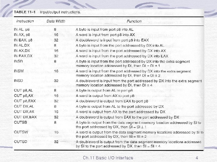
Table 11 -1 Ch. 11 Basic I/O Interface 4
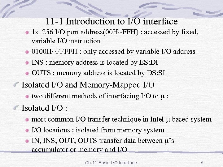
11 -1 Introduction to I/O interface 1 st 256 I/O port address(00 H~FFH) : accessed by fixed, variable I/O instruction 0100 H~FFFFH : only accessed by variable I/O address INS : memory address is located by ES: DI OUTS : memory address is located by DS: SI Isolated I/O and Memory-Mapped I/O two different methods of interfacing I/O to µ : Isolated I/O : most common I/O transfer technique in Intel µ based system I/O locations : isolated from memory system IN, INS, OUTS transfer data between µ’s accumulator or memory and I/O Ch. 11 Basic I/O Interface 5
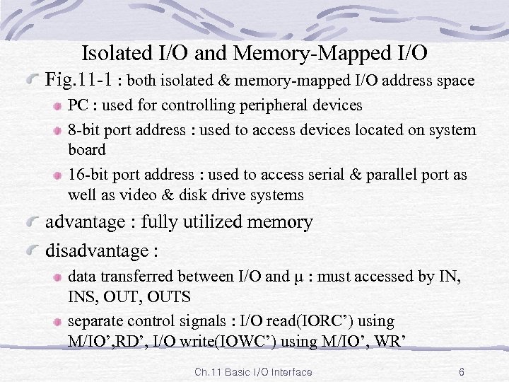
Isolated I/O and Memory-Mapped I/O Fig. 11 -1 : both isolated & memory-mapped I/O address space PC : used for controlling peripheral devices 8 -bit port address : used to access devices located on system board 16 -bit port address : used to access serial & parallel port as well as video & disk drive systems advantage : fully utilized memory disadvantage : data transferred between I/O and µ : must accessed by IN, INS, OUTS separate control signals : I/O read(IORC’) using M/IO’, RD’, I/O write(IOWC’) using M/IO’, WR’ Ch. 11 Basic I/O Interface 6
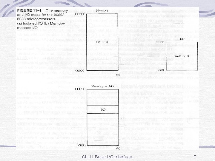
Fig. 11 -1 Ch. 11 Basic I/O Interface 7
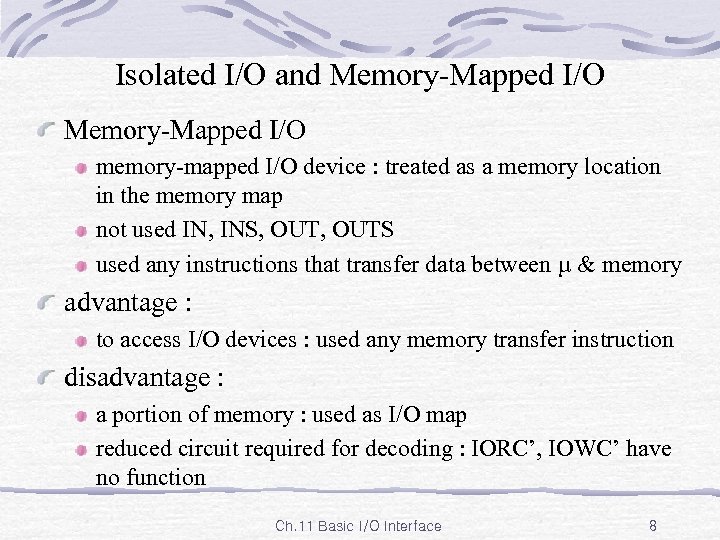
Isolated I/O and Memory-Mapped I/O memory-mapped I/O device : treated as a memory location in the memory map not used IN, INS, OUTS used any instructions that transfer data between µ & memory advantage : to access I/O devices : used any memory transfer instruction disadvantage : a portion of memory : used as I/O map reduced circuit required for decoding : IORC’, IOWC’ have no function Ch. 11 Basic I/O Interface 8
Personal Computer I/O Map Fig. 11 -2 : I/O map for PC 0000 H ~ 03 FFH : reserved for computer system and ISA bus 0400 H ~ FFFFH : for user applications, main-board functions, and PCI bus 00 F 8 H~00 FFH : for communications to coprocessor Basic Input Interface : Fig. 11 -3 3 -state buffers : used to construct 8 -bit input port µ : read contents of 8 switches that connect to any 8 -bit section of data bus when select signal SEL’ = 0 when µ execute IN : I/O port address is decoded to generate the logic 0 on SEL’ Ch. 11 Basic I/O Interface 9
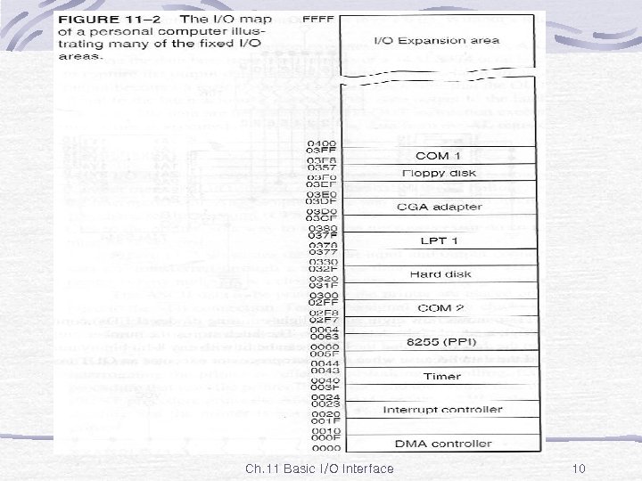
Fig. 11 -2 Ch. 11 Basic I/O Interface 10
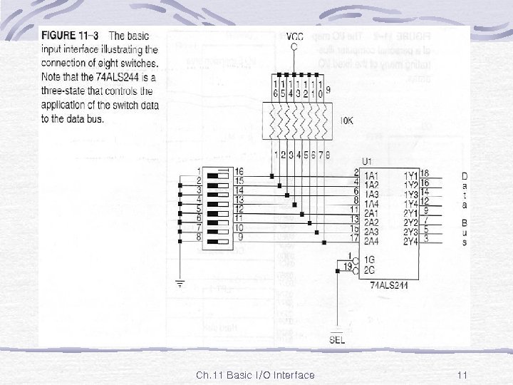
Fig. 11 -3 Ch. 11 Basic I/O Interface 11
Basic Output Interface : Fig. 11 -4 data latches : used to construct 8 -bit output port basic output interface : received data from µ and must usually hold it for some external device when OUT execute : data from accumulator are transferred to latch via data bus Hand Shaking : many I/O : accept or release at a much slower rate than µ another method of I/O control : handshaking(polling) synchronize I/O device with µ parallel printer : print 100 characters per second(CPS) Ch. 11 Basic I/O Interface 12
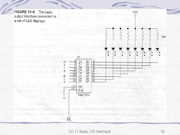
Fig. 11 -4 Ch. 11 Basic I/O Interface 13
Handshaking Fig. 11 -5 : typical input and output of printer D 7~D 0 : data connection BUSY : indicate that printer is busy STB’ : a clock pulse used to send data into printer handshaking(polling) µ poll and test BUSY pin. if busy, µ wait if not busy, ASCII data is placed on D 7~D 0, and pulse is applied to STB’ connection printer received data, placed a logic 1 on BUSY pin Ex. 11 -1 : simple procedure that test printer BUSY flag & send data to printer if not busy Ch. 11 Basic I/O Interface 14
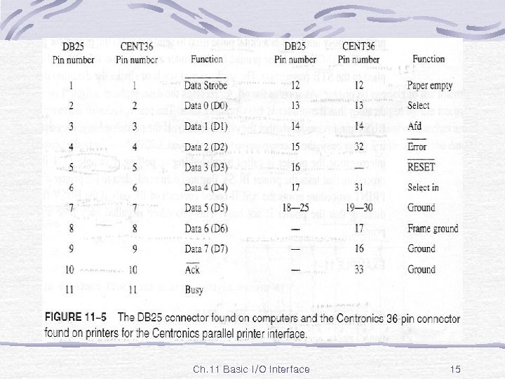
Fig. 11 -5 Ch. 11 Basic I/O Interface 15
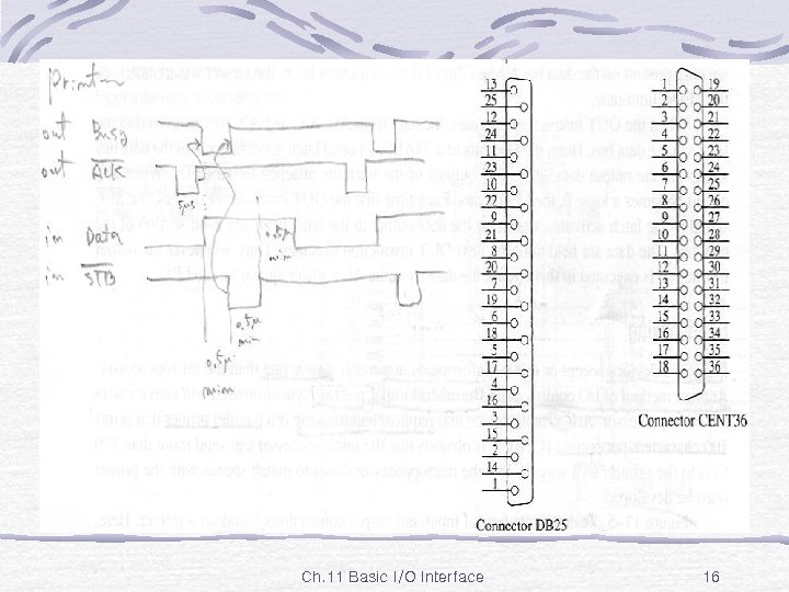
Fig. 11 -5 Ch. 11 Basic I/O Interface 16
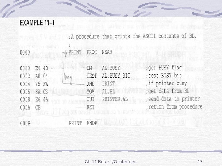
Ex. 11 -1 Ch. 11 Basic I/O Interface 17
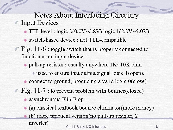
Notes About Interfacing Circuitry Input Devices TTL level : logic 0(0. 0 V~0. 8 V) logic 1(2. 0 V~5. 0 V) switch-based device : not TTL-compatible Fig. 11 -6 : toggle switch that is properly connected to function as an input device pull-up resister : usually anywhere 1 K~10 K ohm used to ensure that output signal logic 1(open), connect to ground, producing a valid logic 0(close) Fig. 11 -7 : to prevent problem with bounce(closed) asynchronous Flip-Flop (a) classical textbook bounce eliminator(more money) (b) more practical version(no pull-up resister, 2 inverter) Ch. 11 Basic I/O Interface 18
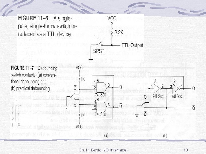
Fig. 11 -6 Ch. 11 Basic I/O Interface 19
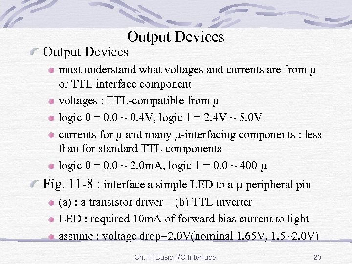
Output Devices must understand what voltages and currents are from µ or TTL interface component voltages : TTL-compatible from µ logic 0 = 0. 0 ~ 0. 4 V, logic 1 = 2. 4 V ~ 5. 0 V currents for µ and many µ-interfacing components : less than for standard TTL components logic 0 = 0. 0 ~ 2. 0 m. A, logic 1 = 0. 0 ~ 400 µ Fig. 11 -8 : interface a simple LED to a µ peripheral pin (a) : a transistor driver (b) TTL inverter LED : required 10 m. A of forward bias current to light assume : voltage drop=2. 0 V(nominal 1. 65 V, 1. 5~2. 0 V) Ch. 11 Basic I/O Interface 20
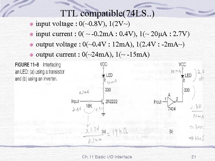
TTL compatible(74 LS. . ) input voltage : 0(~0. 8 V), 1(2 V~) input current : 0( ~ -0. 2 m. A : 0. 4 V), 1(~ 20 A : 2. 7 V) output voltage : 0(~0. 4 V : 12 m. A), 1(2. 4 V : -2 m. A~) output current : 0(~24 m. A), 1(~ -15 m. A) Ch. 11 Basic I/O Interface 21
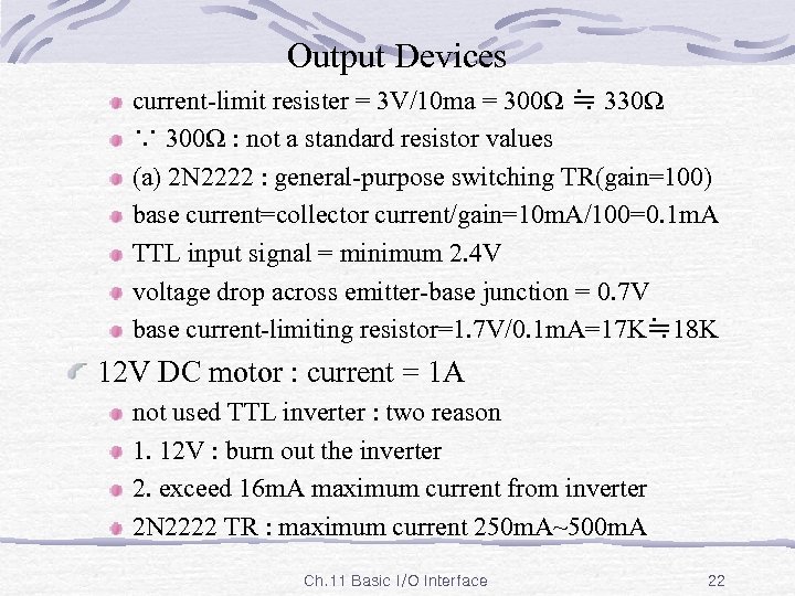
Output Devices current-limit resister = 3 V/10 ma = 300Ω ≒ 330Ω ∵ 300Ω : not a standard resistor values (a) 2 N 2222 : general-purpose switching TR(gain=100) base current=collector current/gain=10 m. A/100=0. 1 m. A TTL input signal = minimum 2. 4 V voltage drop across emitter-base junction = 0. 7 V base current-limiting resistor=1. 7 V/0. 1 m. A=17 K≒ 18 K 12 V DC motor : current = 1 A not used TTL inverter : two reason 1. 12 V : burn out the inverter 2. exceed 16 m. A maximum current from inverter 2 N 2222 TR : maximum current 250 m. A~500 m. A Ch. 11 Basic I/O Interface 22
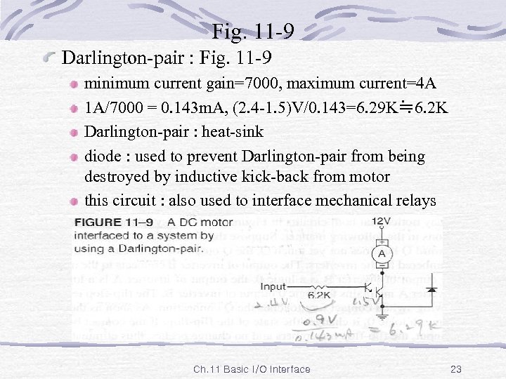
Fig. 11 -9 Darlington-pair : Fig. 11 -9 minimum current gain=7000, maximum current=4 A 1 A/7000 = 0. 143 m. A, (2. 4 -1. 5)V/0. 143=6. 29 K≒ 6. 2 K Darlington-pair : heat-sink diode : used to prevent Darlington-pair from being destroyed by inductive kick-back from motor this circuit : also used to interface mechanical relays Ch. 11 Basic I/O Interface 23
11 -2 I/O Port Address Decoding similar to memory address decoding, especially for memory-mapped I/O main difference : between memory decoding & isolated I/O decoding no of address pins connected to the decoder memory(A 31~, A 23~, A 19~A 0), isolated I/O(A 15~A 0) used only fixed I/O addressing : decode only A 7~A 0 another difference : use IORC’, IOWC’(M/IO’, RD’, WR’) Decoding 8 -bit I/O addresses fixed I/O instruction : used 8 -bit I/O port address that appear on A 15~A 0 as 0000 H~00 FFH Ch. 11 Basic I/O Interface 24
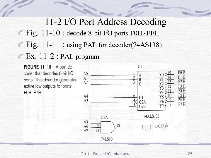
11 -2 I/O Port Address Decoding Fig. 11 -10 : decode 8 -bit I/O ports F 0 H~FFH Fig. 11 -11 : using PAL for decoder(74 AS 138) Ex. 11 -2 : PAL program Ch. 11 Basic I/O Interface 25
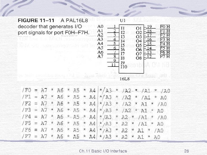
Fig. 11 -11 Ch. 11 Basic I/O Interface 26
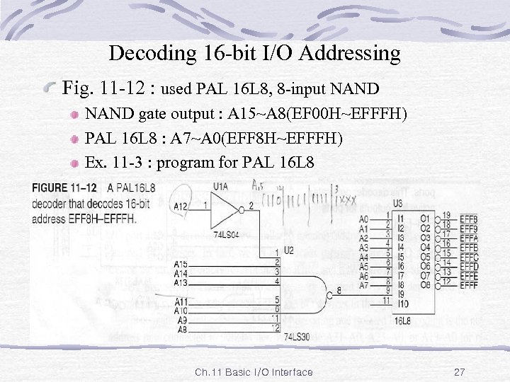
Decoding 16 -bit I/O Addressing Fig. 11 -12 : used PAL 16 L 8, 8 -input NAND gate output : A 15~A 8(EF 00 H~EFFFH) PAL 16 L 8 : A 7~A 0(EFF 8 H~EFFFH) Ex. 11 -3 : program for PAL 16 L 8 Ch. 11 Basic I/O Interface 27
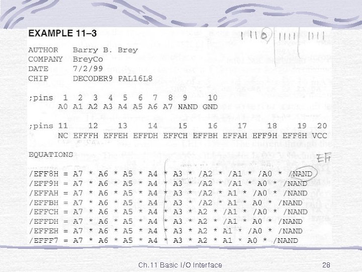
Ex. 11 -3 Ch. 11 Basic I/O Interface 28
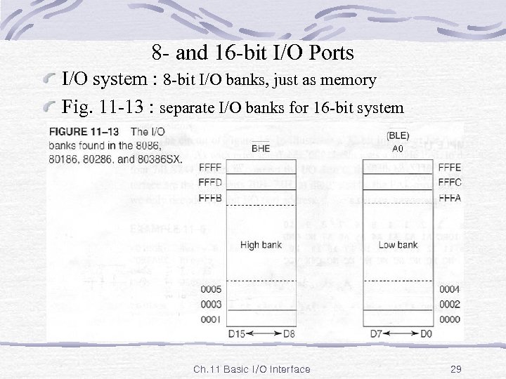
8 - and 16 -bit I/O Ports I/O system : 8 -bit I/O banks, just as memory Fig. 11 -13 : separate I/O banks for 16 -bit system Ch. 11 Basic I/O Interface 29
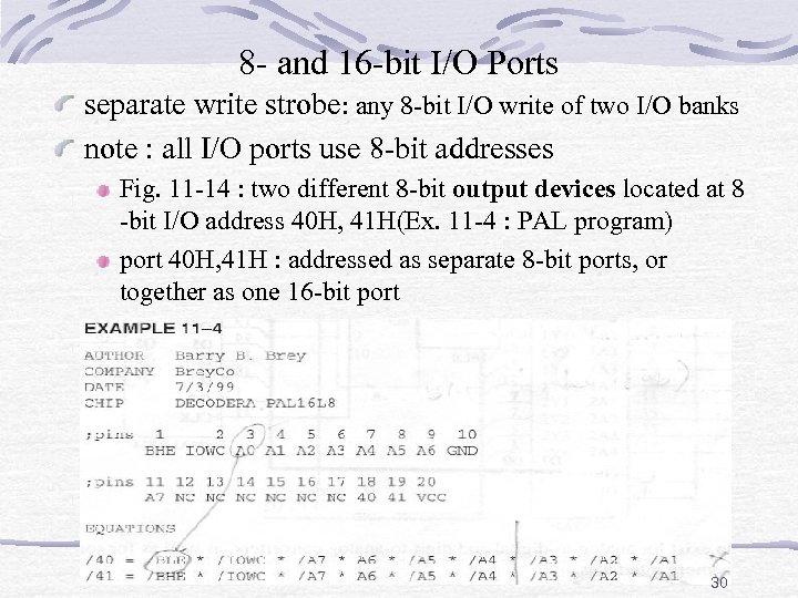
8 - and 16 -bit I/O Ports separate write strobe: any 8 -bit I/O write of two I/O banks note : all I/O ports use 8 -bit addresses Fig. 11 -14 : two different 8 -bit output devices located at 8 -bit I/O address 40 H, 41 H(Ex. 11 -4 : PAL program) port 40 H, 41 H : addressed as separate 8 -bit ports, or together as one 16 -bit port 30
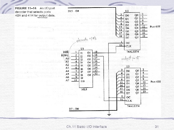
Fig. 11 -14 Ch. 11 Basic I/O Interface 31
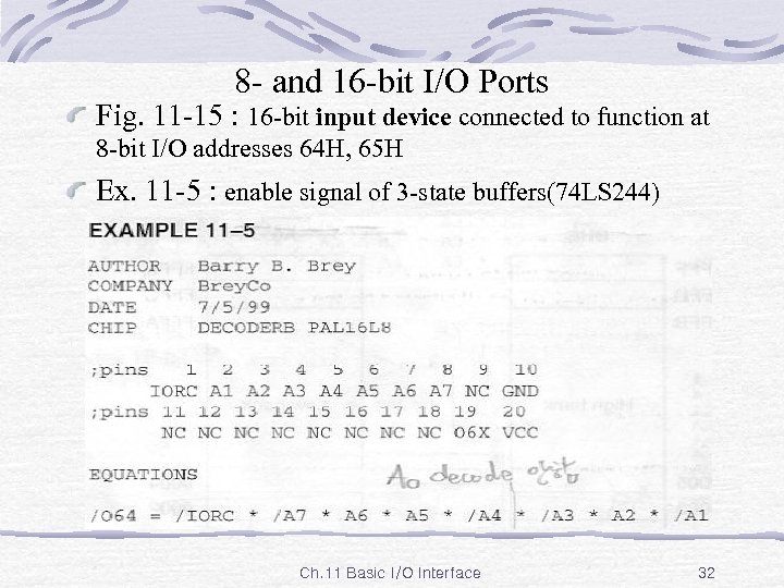
8 - and 16 -bit I/O Ports Fig. 11 -15 : 16 -bit input device connected to function at 8 -bit I/O addresses 64 H, 65 H Ex. 11 -5 : enable signal of 3 -state buffers(74 LS 244) Ch. 11 Basic I/O Interface 32
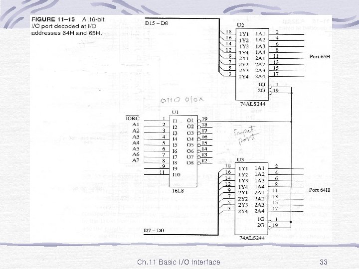
Fig. 11 -15 Ch. 11 Basic I/O Interface 33
32 -bit Wide I/O Ports 32 -bit wide I/O port : not common eventually become commonplace because newer buses EISA system bus, VESA local, current PCI bus Fig. 11 -16: 32 -bit input port for 32 -bit µ(8 -bit port 70~73 H) Ex. 11 -6 : PAL program /SEL=/IORC*/A 7*A 6*A 5*A 4*/A 3*/A 2=0111 00 xx 64 -bit Pentium µ : 8 -bit I/O port 0034 H : Pentium I/O bank 5 16 -bit I/O port 0034 H~0035 H : I/O bank 5, 6 32 -bit I/O port 0100 H~0103 H : I/O bank 0~3 widest I/O transfer : 32 bits, no 64 -bit I/O instructions Ch. 11 Basic I/O Interface 34
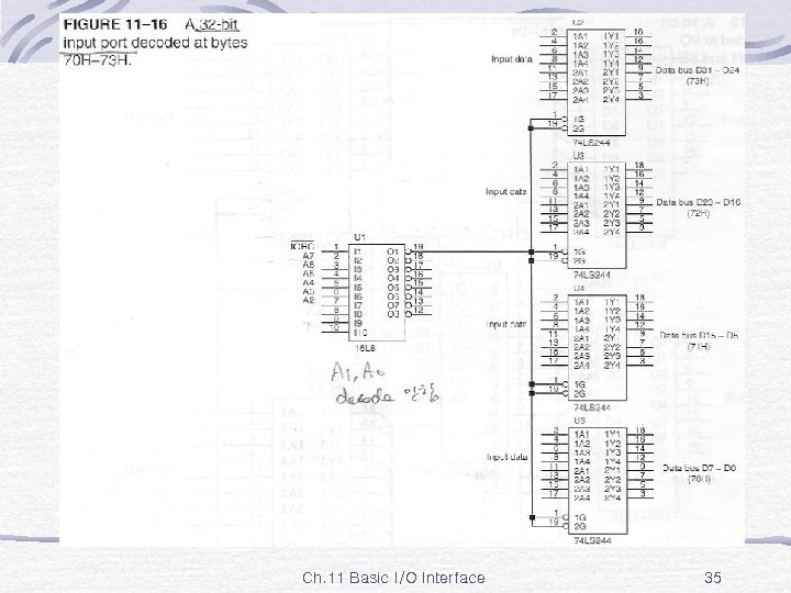
Fig. 11 -16 Ch. 11 Basic I/O Interface 35
11 -3 The Programmable Peripheral Interface 82 C 55 PPI : programmable peripheral interface very popular, low-cost interfacing component 24 pins for I/O : programmable in groups of 12 pins groups that operate in three distinct modes of operation interface any TTL-compatible I/O device to µ require wait states if operated with µ higher than 8 MHz provided at least 2. 5 m. A of sink current at each output, with a maximum of 4. 0 m. A Fig. 11 -17 : pin-out diagram three I/O ports A, B, C : programmed as group A : port A(PA 7~PA 0), PC 7~PC 4 of port C group B : port B(PB 7~PB 0), PC 3~PC 0 of port C Ch. 11 Basic I/O Interface 36
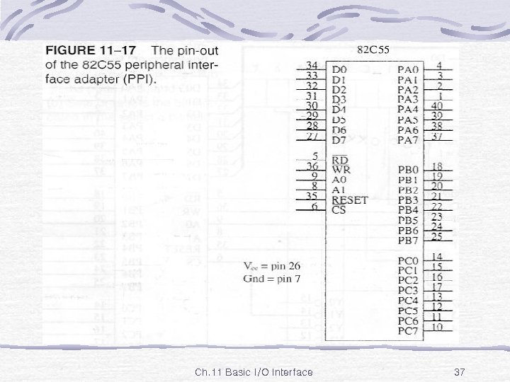
Fig. 11 -17 Ch. 11 Basic I/O Interface 37
11 -3 The Programmable Peripheral Interface A 1~A 0 : select an internal register for programming or operation(Table 11 -2) PC system : 82 C 55 is decoded at I/O ports 60 H~63 H for keyboard control, for controlling speaker, timer Fig. 11 -18 : 82 C 55 connected to 80386 SX 8 -bit I/O port addresses C 0 H(port A), C 2 H(port B), C 4 H(port C), C 6 H(command register) interfaced low bank of 80386 SX I/O map RESET : initialized 82 C 55 whenever µ is reset all ports : set up as simple input ports using mode 0 internally programmed input pins after RESET damage: prevented when power is 1 st applied to system Ch. 11 Basic I/O Interface 38
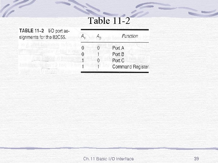
Table 11 -2 Ch. 11 Basic I/O Interface 39
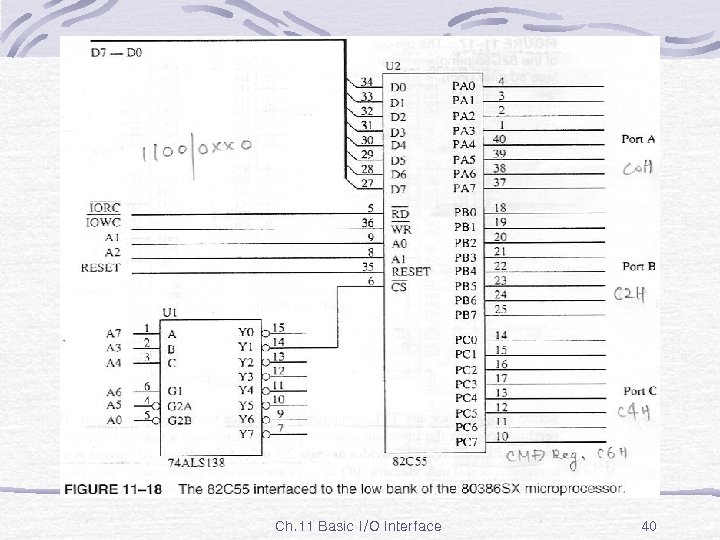
Fig. 11 -18 Ch. 11 Basic I/O Interface 40
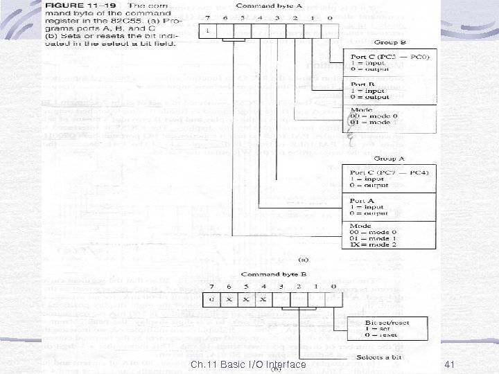
Fig. 11 -19 Ch. 11 Basic I/O Interface 41
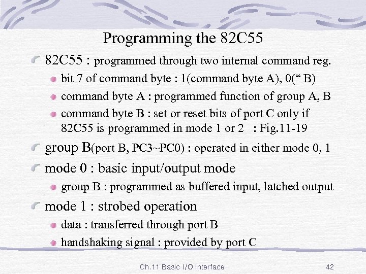
Programming the 82 C 55 : programmed through two internal command reg. bit 7 of command byte : 1(command byte A), 0(“ B) command byte A : programmed function of group A, B command byte B : set or reset bits of port C only if 82 C 55 is programmed in mode 1 or 2 : Fig. 11 -19 group B(port B, PC 3~PC 0) : operated in either mode 0, 1 mode 0 : basic input/output mode group B : programmed as buffered input, latched output mode 1 : strobed operation data : transferred through port B handshaking signal : provided by port C Ch. 11 Basic I/O Interface 42
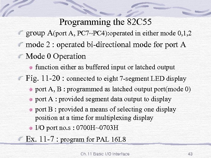
Programming the 82 C 55 group A(port A, PC 7~PC 4): operated in either mode 0, 1, 2 mode 2 : operated bi-directional mode for port A Mode 0 Operation function either as buffered input or latched output Fig. 11 -20 : connected to eight 7 -segment LED display port A, B : programmed as latched output port(mode 0) port A : provided segment data output to display port B : provided a means of selecting one display position at a time for multiplexing display I/O port no. s : 0700 H~0703 H Ex. 11 -7 : program for PAL 16 L 8 Ch. 11 Basic I/O Interface 43
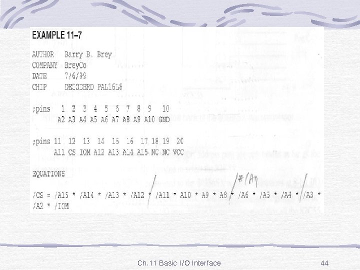
Ex. 11 -7 Ch. 11 Basic I/O Interface 44
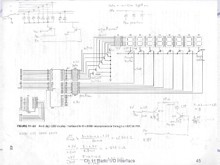
Fig. 11 -20 Ch. 11 Basic I/O Interface 45
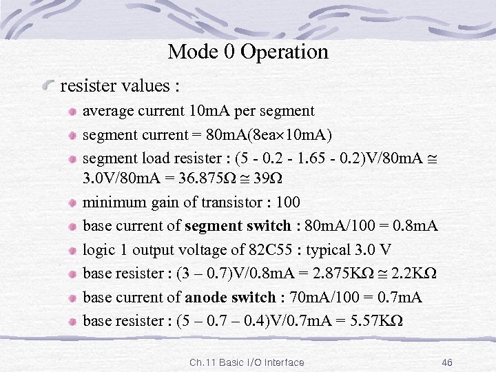
Mode 0 Operation resister values : average current 10 m. A per segment current = 80 m. A(8 ea 10 m. A) segment load resister : (5 - 0. 2 - 1. 65 - 0. 2)V/80 m. A 3. 0 V/80 m. A = 36. 875Ω 39Ω minimum gain of transistor : 100 base current of segment switch : 80 m. A/100 = 0. 8 m. A logic 1 output voltage of 82 C 55 : typical 3. 0 V base resister : (3 – 0. 7)V/0. 8 m. A = 2. 875 KΩ 2. 2 KΩ base current of anode switch : 70 m. A/100 = 0. 7 m. A base resister : (5 – 0. 7 – 0. 4)V/0. 7 m. A = 5. 57 KΩ Ch. 11 Basic I/O Interface 46
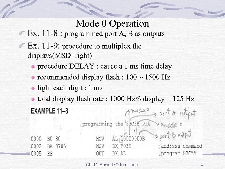
Mode 0 Operation Ex. 11 -8 : programmed port A, B as outputs Ex. 11 -9: procedure to multiplex the displays(MSD=right) procedure DELAY : cause a 1 ms time delay recommended display flash : 100 ~ 1500 Hz light each digit : 1 ms total display flash rate : 1000 Hz/8 display = 125 Hz eight 7 -segment code : stored at MEM ~ MEM+7(MSD) Ch. 11 Basic I/O Interface 47
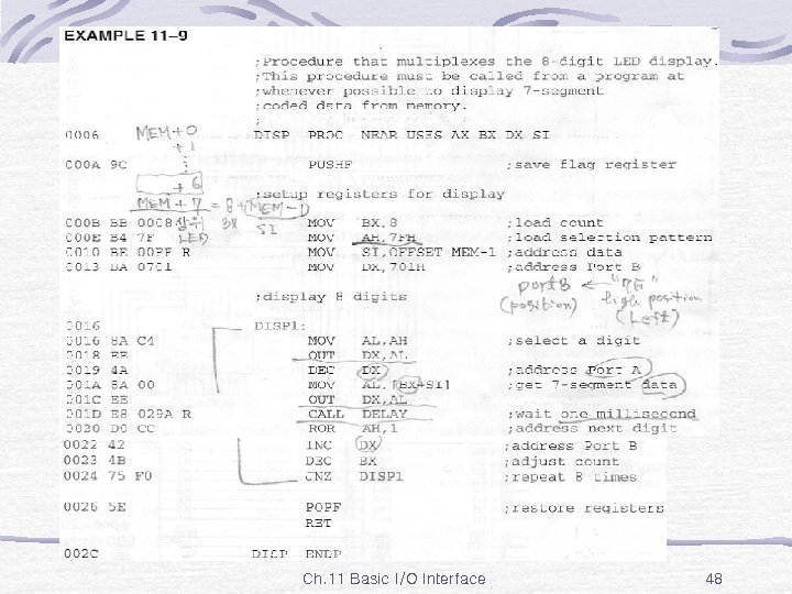
Ex. 11 -9 Ch. 11 Basic I/O Interface 48
An LCD Display Interfaced to the 82 C 55 LCD(liquid crystal display) : quickly replacing LED disadvantage : difficult to see in low-light situations Fig. 11 -21 : Optrex DMC-20481(4 line 20 ch. ) LCD accept ASCII code as input data also accept command to initialize, control its application data connections : attached to 82 C 55 port A used to input display data and to output information from display four control pins : VEE, RS, E, R/W’ VEE : to adjust the contrast of LCD normally connected to 10 K potentiometer Ch. 11 Basic I/O Interface 49
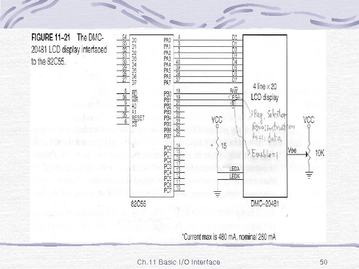
Fig. 11 -21 Ch. 11 Basic I/O Interface 50
An LCD Display Interfaced to the 82 C 55 RS(resister select) : data(RS=1) or instructions(RS=0) E(enable) : logic 1 to read or write information R/W’ : select a read or a write operation two inputs for back-lighting LED, which not shown normally, RS(1 or 0), R/W’(1 or 0), data input pins(data) and then E pin is pulsed to access the LCD initialization : accomplished via following steps 1. wait at least 15 ms after Vcc rise to 5. 0 V 2. output function set command(30 H), wait at least 4. 1 ms 3. output function set command(30 H) a second time, wait at least 100 ㎲ Ch. 11 Basic I/O Interface 51
An LCD Display Interfaced to the 82 C 55 4. output function set command(30 H) a third time, wait at least 40 ㎲ 5. output function set command(38 H) a fourth time, wait at least 40 ㎲ 6. output a 08 H to disable display, wait at least 40 ㎲ 7. output a 01 H to home cursor and clear display, wait at least 1. 64 ms 8. output the enable display cursor off(0 CH), wait at least 40 ㎲ 9. output a 06 H to select auto-increment, shift cursor, wait at least 40 ㎲ Ch. 11 Basic I/O Interface 52
An LCD Display Interfaced to the 82 C 55 Ex. 11 -10 : initialization three time delays : DELAY 15, DELAY 41, DELAY 100 clock tick : used for all timing NOP(in OUTCMD procedure) : to ensure that E bit remain a logic 1 long enough to activate LCD display Table 11 -3 : command used in initialization dialog to display information and control the display : needed a few procedure no longer needed time delay : test busy flag bit Ex. 11 -11 : BUSY procedure test LCD and only return when display has completely a prior instruction Ch. 11 Basic I/O Interface 53
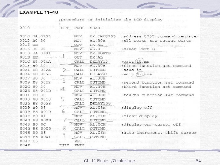
Ex. 11 -10 Ch. 11 Basic I/O Interface 54
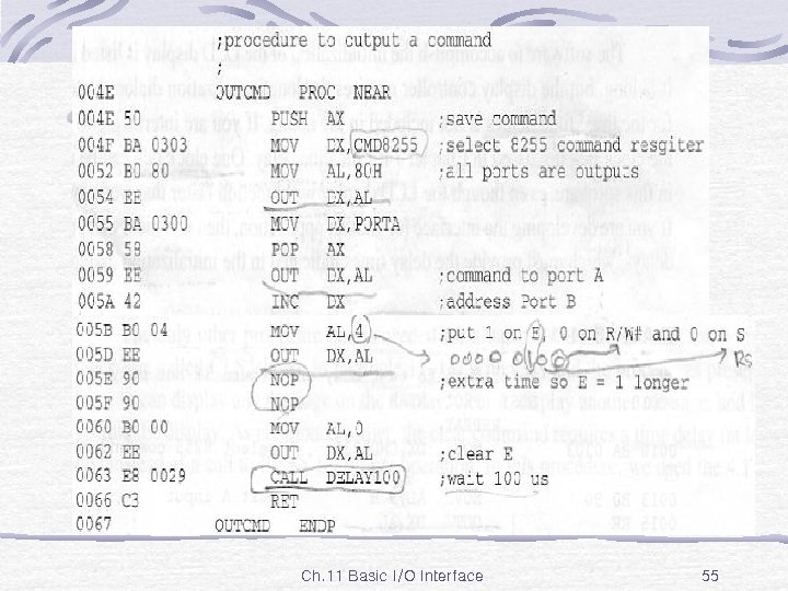
Ex. 11 -10 Ch. 11 Basic I/O Interface 55
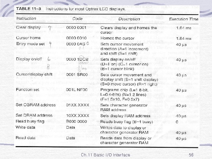
Table 11 -3 Ch. 11 Basic I/O Interface 56
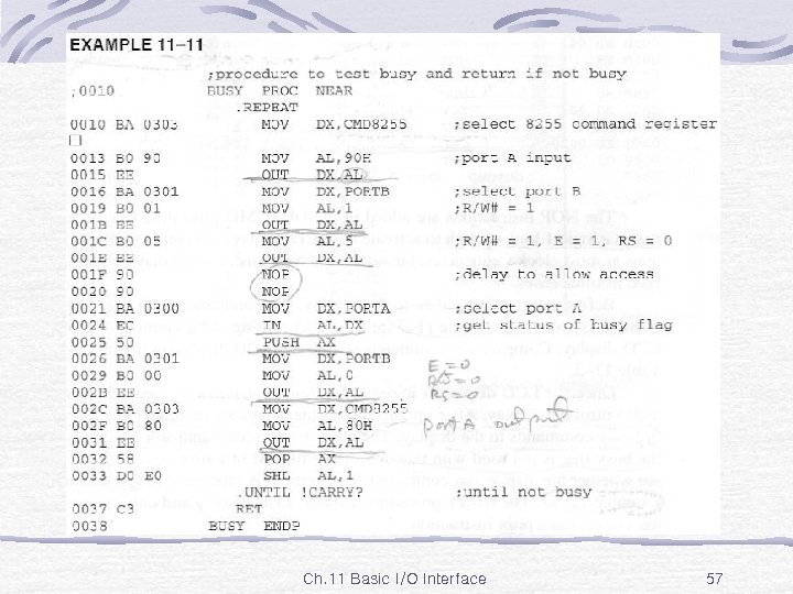
Ex. 11 -11 Ch. 11 Basic I/O Interface 57
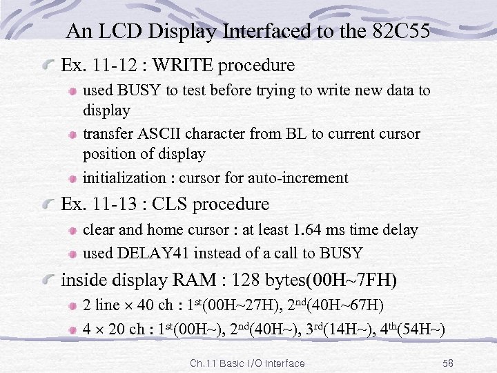
An LCD Display Interfaced to the 82 C 55 Ex. 11 -12 : WRITE procedure used BUSY to test before trying to write new data to display transfer ASCII character from BL to current cursor position of display initialization : cursor for auto-increment Ex. 11 -13 : CLS procedure clear and home cursor : at least 1. 64 ms time delay used DELAY 41 instead of a call to BUSY inside display RAM : 128 bytes(00 H~7 FH) 2 line 40 ch : 1 st(00 H~27 H), 2 nd(40 H~67 H) 4 20 ch : 1 st(00 H~), 2 nd(40 H~), 3 rd(14 H~), 4 th(54 H~) Ch. 11 Basic I/O Interface 58
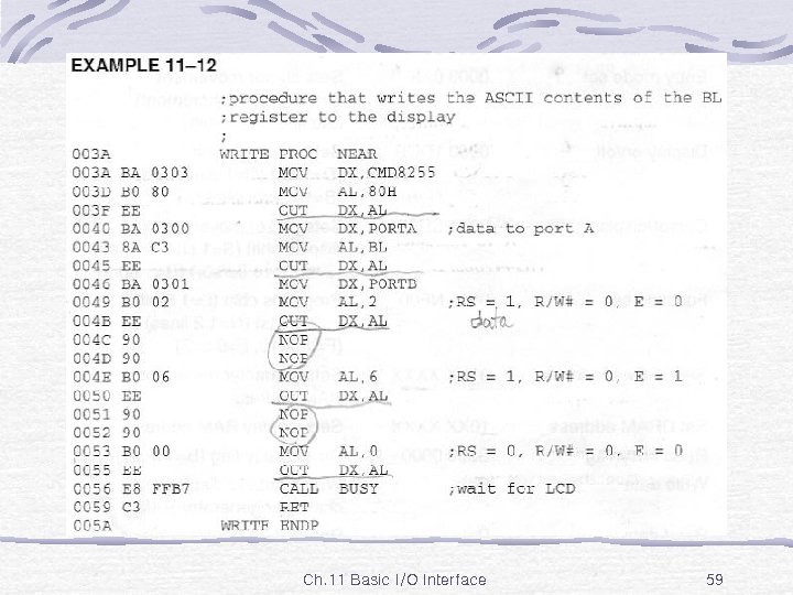
Ex. 11 -12 Ch. 11 Basic I/O Interface 59
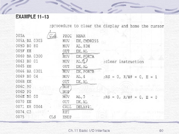
Ex. 11 -13 Ch. 11 Basic I/O Interface 60
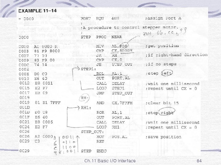
A Stepper Motor Interfaced to the 82 C 55 stepper motor : digital motor because it is moved in discrete steps as it traverse through 360° geared to move 15°(common)~1° per step(high-precision) steps: gained through many magnetic poles and/or gearing Fig. 11 -22 : four-coil step motor that use an armature with a single pole(energized two coils : 45°, 135°, 225°, 315°) Fig. 11 -23 : stepper motor interfaced to 82 C 55 driven by using NPN Darlington amplifier pairs to provide a large current to each coil Ex. 11 -14 : procedure(port A : programmed in mode 0) CX : hold no of steps and direction of rotation Ch. 11 Basic I/O Interface 61
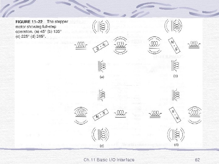
Fig. 11 -22 Ch. 11 Basic I/O Interface 62
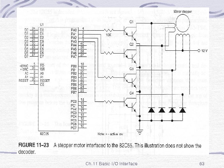
Fig. 11 -23 Ch. 11 Basic I/O Interface 63
Ex. 11 -14 Ch. 11 Basic I/O Interface 64
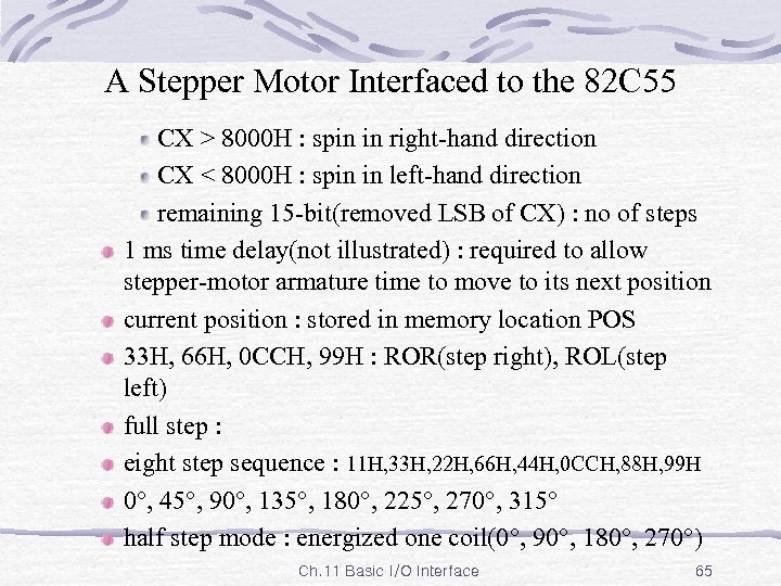
A Stepper Motor Interfaced to the 82 C 55 CX > 8000 H : spin in right-hand direction CX < 8000 H : spin in left-hand direction remaining 15 -bit(removed LSB of CX) : no of steps 1 ms time delay(not illustrated) : required to allow stepper-motor armature time to move to its next position current position : stored in memory location POS 33 H, 66 H, 0 CCH, 99 H : ROR(step right), ROL(step left) full step : eight step sequence : 11 H, 33 H, 22 H, 66 H, 44 H, 0 CCH, 88 H, 99 H 0°, 45°, 90°, 135°, 180°, 225°, 270°, 315° half step mode : energized one coil(0°, 90°, 180°, 270°) Ch. 11 Basic I/O Interface 65
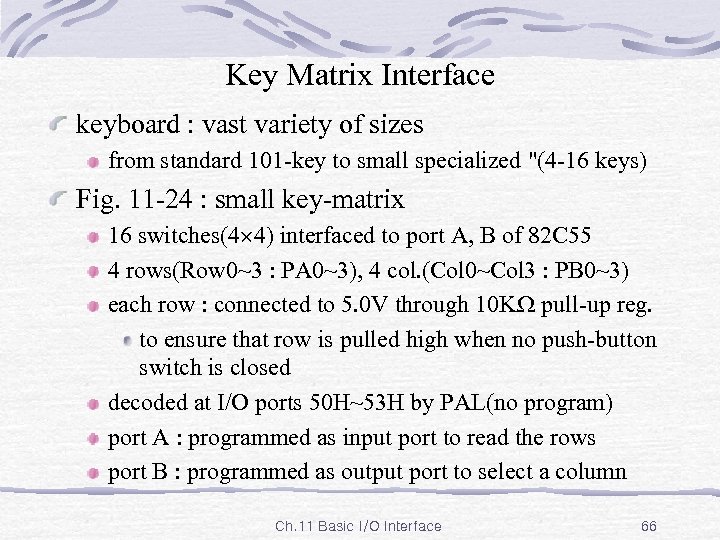
Key Matrix Interface keyboard : vast variety of sizes from standard 101 -key to small specialized "(4 -16 keys) Fig. 11 -24 : small key-matrix 16 switches(4 4) interfaced to port A, B of 82 C 55 4 rows(Row 0~3 : PA 0~3), 4 col. (Col 0~Col 3 : PB 0~3) each row : connected to 5. 0 V through 10 K pull-up reg. to ensure that row is pulled high when no push-button switch is closed decoded at I/O ports 50 H~53 H by PAL(no program) port A : programmed as input port to read the rows port B : programmed as output port to select a column Ch. 11 Basic I/O Interface 66
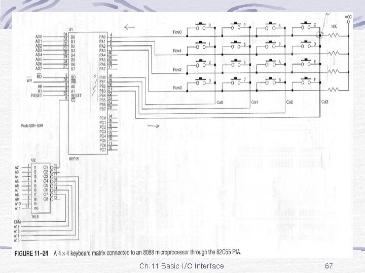
Fig. 11 -24 Ch. 11 Basic I/O Interface 67
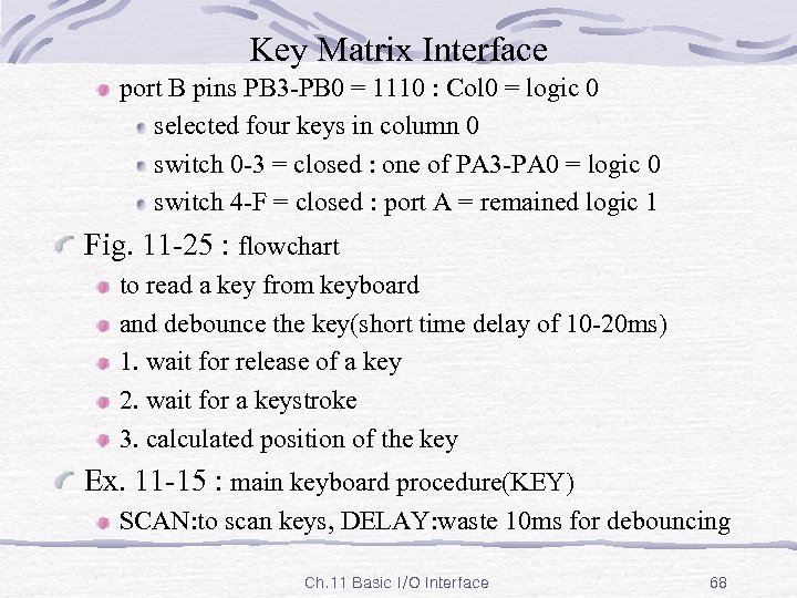
Key Matrix Interface port B pins PB 3 -PB 0 = 1110 : Col 0 = logic 0 selected four keys in column 0 switch 0 -3 = closed : one of PA 3 -PA 0 = logic 0 switch 4 -F = closed : port A = remained logic 1 Fig. 11 -25 : flowchart to read a key from keyboard and debounce the key(short time delay of 10 -20 ms) 1. wait for release of a key 2. wait for a keystroke 3. calculated position of the key Ex. 11 -15 : main keyboard procedure(KEY) SCAN: to scan keys, DELAY: waste 10 ms for debouncing Ch. 11 Basic I/O Interface 68
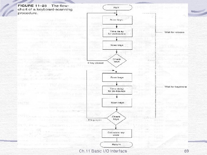
Fig. 11 -25 Ch. 11 Basic I/O Interface 69
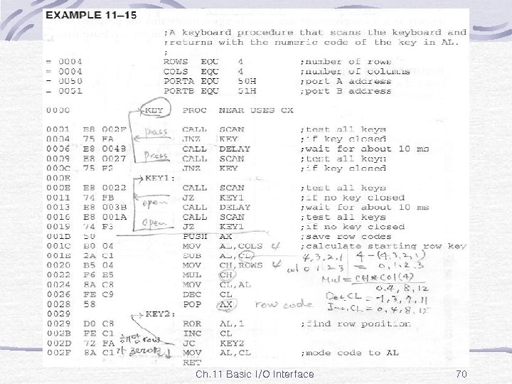
Ex. 11 -15 Ch. 11 Basic I/O Interface 70
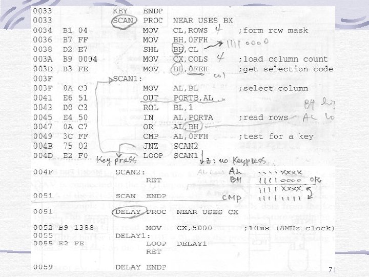
Ex. 11 -15 71
Mode 1 Strobed Input Mode 1 : Fig. 11 -26 port A and/or port B to function as latching input devices port C : used for control or handshaking signal definition for mode 1 strobed input : STB’(strobe) input : capture external data into port latch on 0 -to-1 transition activate IBF(input buffer full), INTR(interrupt request) port latch : hold data until µ read it via IN instruction µ : notice through software(IBF) or hardware(INTR) IBF output : indicated that input latch contain information INTR output : requested an interrupt =1: when STB’ return to 1, =0: when µ read data via IN Ch. 11 Basic I/O Interface 72
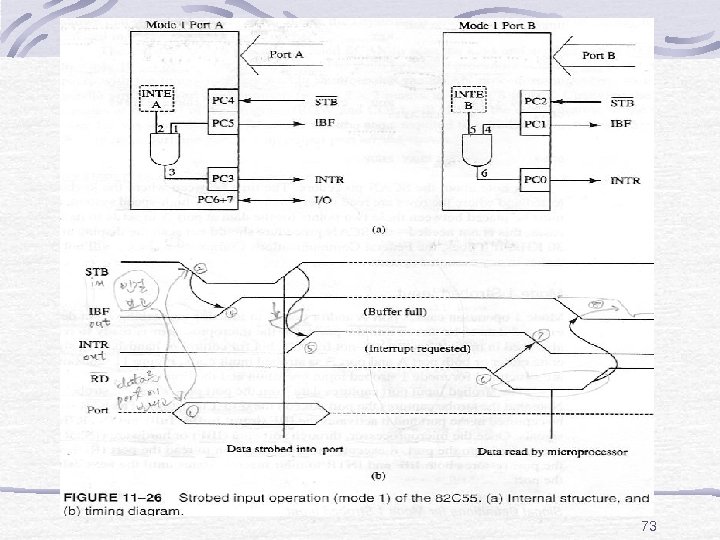
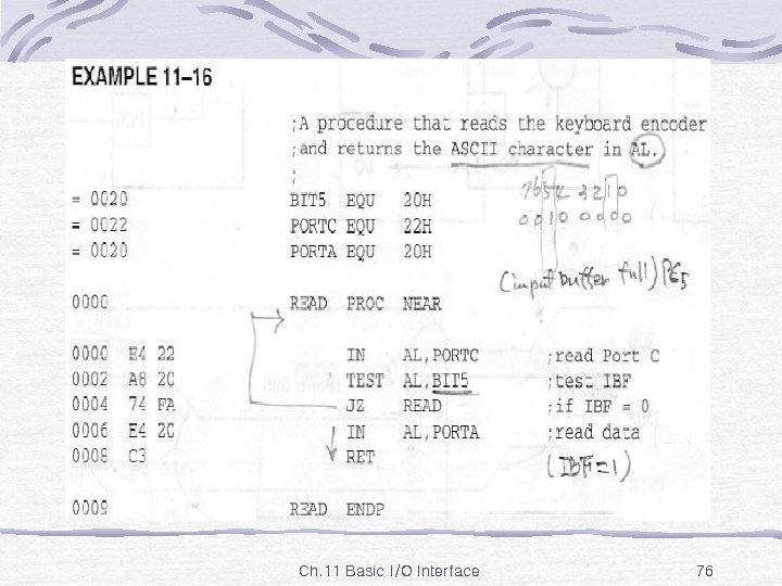
Fig. 11 -26 73
Mode 1 Strobed Input INTE(interrupt enable) signal : neither input nor output internal bit programmed via PC 4(port A), PC 2(port B) PC 7, PC 6 : available for any general-purpose I/O keyboard : excellent example of strobed input device debounced a key-switches provided strobed signal whenever a key is depressed data output contained the ASCII-coded key code Fig. 11 -27 : keyboard connected to strobed input port A DAV’(data available) : connected to STB’ activated for 1. 0µs each time that a key is typed each time a key is typed : data is stored into port A Ex. 11 -16 : procedure Ch. 11 Basic I/O Interface 74
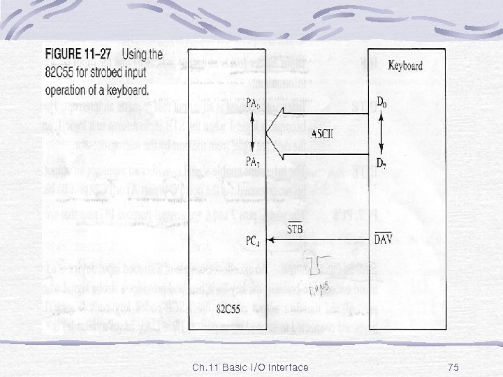
Fig. 11 -27 Ch. 11 Basic I/O Interface 75
Ex. 11 -16 Ch. 11 Basic I/O Interface 76
Mode 1 Strobed Output Fig. 11 -28 : signal definition for mode 1 strobed output : OBF’(output buffer full) output : 0: whenever data are output(OUT) to port A, B latch 1: whenever ACK’ pulse return from external device ACK’(acknowledge) input : indicate that external device has received the data from 82 C 55 port INTR output : often requested an interrupt when external devices receive data via ACK’ qualified by internal INTE’ bit INTE’ : neither input nor output internal programmed bit via PC 6(port A), PC 2(port B) Ch. 11 Basic I/O Interface 77
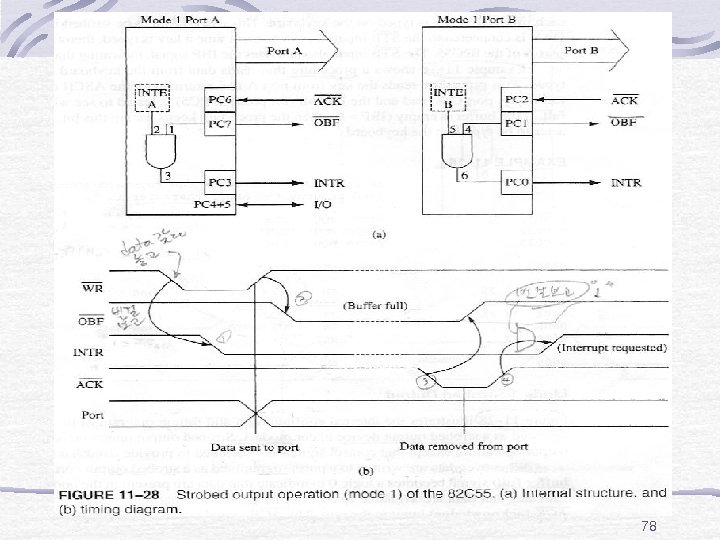
Fig. 11 -28 78
Mode 1 Strobed Output PC 5, PC 4 : general-purpose I/O pins printerface(Fig. 11 -29) : strobed output example port B : connected to parallel printer PC 2 : ACK’ to acknowledge the receipt of ASCII ch. DS’(data strobe) to strobe data into printer PC 4 : used with software that generate DS’ signal Ex. 11 -17 : software that send ASCII-coded character in AH to printer 1. test OBF’, if not wait if OBF’=1 : send AH to printer through port B and also send DS’ signal Ch. 11 Basic I/O Interface 79
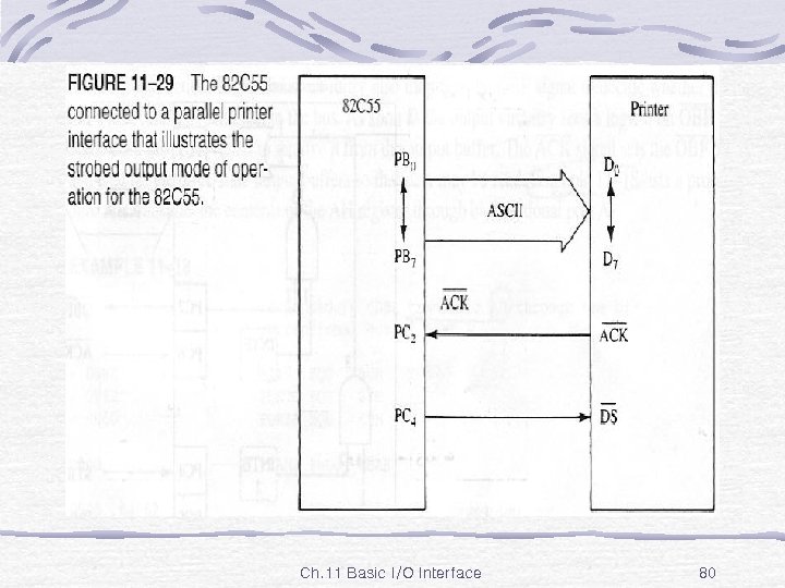
Fig. 11 -29 Ch. 11 Basic I/O Interface 80
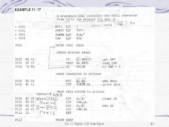
Ex. 11 -17 Ch. 11 Basic I/O Interface 81
Mode 2 Bi-directional Operation port A only : bi-directional mode 1 strobed input and output useful when interfacing two computers used for IEEE-488 parallel high-speed GPIB(general purpose instrumentation bus) interface standard Fig. 11 -30 : the bi-directional bus used by referencing port A with IN, OUT instructions Ex. 11 -18 : to transmit data through bi-directional bus Ex. 11 -19 : to receive data through bi-directional bus INTR : activated from both directions of data flow Ch. 11 Basic I/O Interface 82
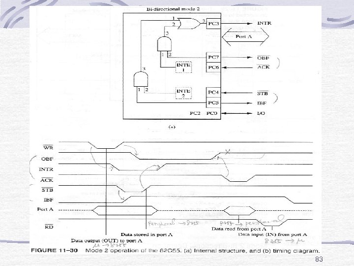
Fig. 11 -30 83
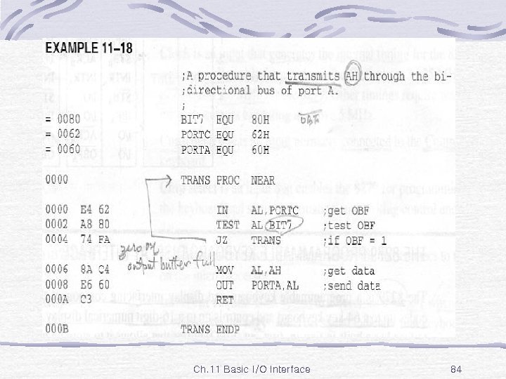
Ex. 11 -18 Ch. 11 Basic I/O Interface 84
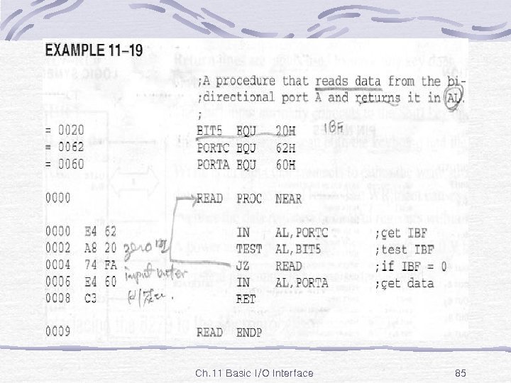
Ex. 11 -19 Ch. 11 Basic I/O Interface 85
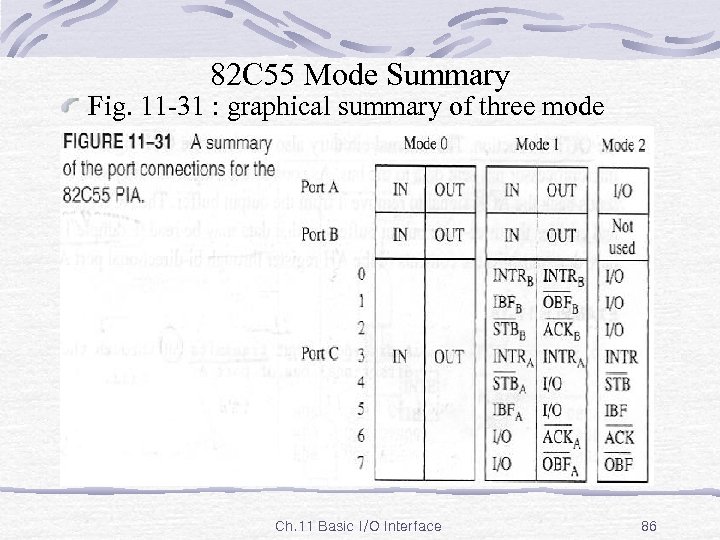
82 C 55 Mode Summary Fig. 11 -31 : graphical summary of three mode Ch. 11 Basic I/O Interface 86
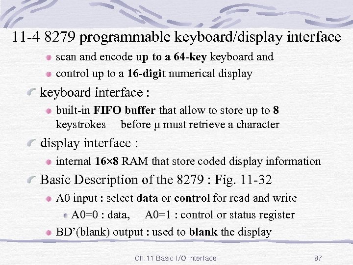
11 -4 8279 programmable keyboard/display interface scan and encode up to a 64 -key keyboard and control up to a 16 -digit numerical display keyboard interface : built-in FIFO buffer that allow to store up to 8 keystrokes before µ must retrieve a character display interface : internal 16 8 RAM that store coded display information Basic Description of the 8279 : Fig. 11 -32 A 0 input : select data or control for read and write A 0=0 : data, A 0=1 : control or status register BD’(blank) output : used to blank the display Ch. 11 Basic I/O Interface 87
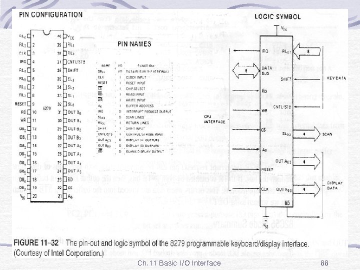
Fig. 11 -32 Ch. 11 Basic I/O Interface 88
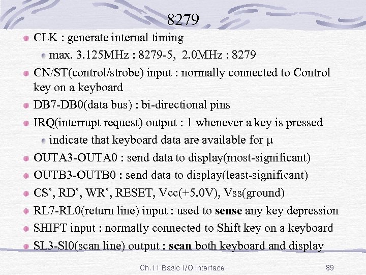
8279 CLK : generate internal timing max. 3. 125 MHz : 8279 -5, 2. 0 MHz : 8279 CN/ST(control/strobe) input : normally connected to Control key on a keyboard DB 7 -DB 0(data bus) : bi-directional pins IRQ(interrupt request) output : 1 whenever a key is pressed indicate that keyboard data are available for µ OUTA 3 -OUTA 0 : send data to display(most-significant) OUTB 3 -OUTB 0 : send data to display(least-significant) CS’, RD’, WR’, RESET, Vcc(+5. 0 V), Vss(ground) RL 7 -RL 0(return line) input : used to sense any key depression SHIFT input : normally connected to Shift key on a keyboard SL 3 -Sl 0(scan line) output : scan both keyboard and display Ch. 11 Basic I/O Interface 89
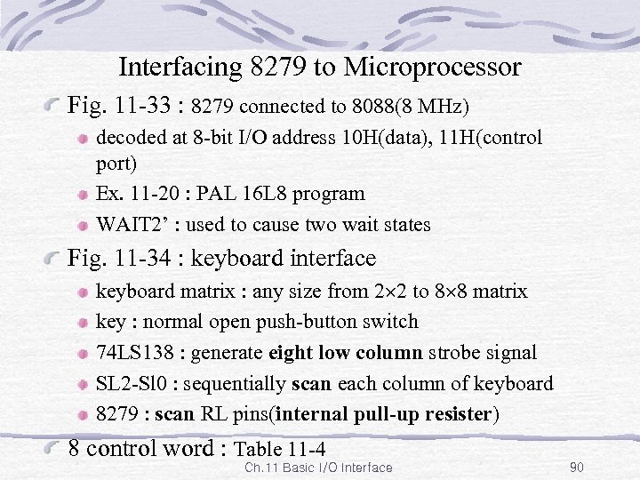
Interfacing 8279 to Microprocessor Fig. 11 -33 : 8279 connected to 8088(8 MHz) decoded at 8 -bit I/O address 10 H(data), 11 H(control port) Ex. 11 -20 : PAL 16 L 8 program WAIT 2’ : used to cause two wait states Fig. 11 -34 : keyboard interface keyboard matrix : any size from 2 2 to 8 8 matrix key : normal open push-button switch 74 LS 138 : generate eight low column strobe signal SL 2 -Sl 0 : sequentially scan each column of keyboard 8279 : scan RL pins(internal pull-up resister) 8 control word : Table 11 -4 Ch. 11 Basic I/O Interface 90
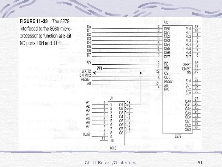
Fig. 11 -33 Ch. 11 Basic I/O Interface 91
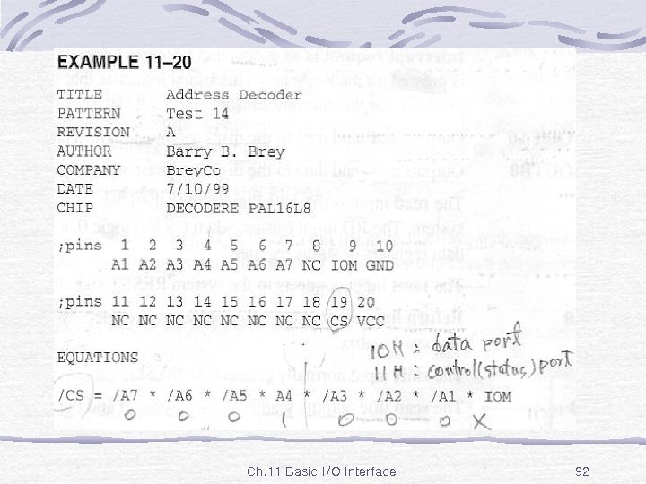
Ex. 11 -20 Ch. 11 Basic I/O Interface 92
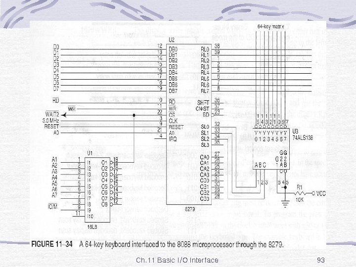
Fig. 11 -34 Ch. 11 Basic I/O Interface 93
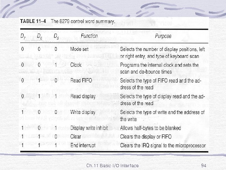
Table 11 -4 Ch. 11 Basic I/O Interface 94
8279 Control Word 000 DD MMM : mode set DD : select mode of operation for display(Table 11 -5) select 8 - or 16 -digit display determine whether new data are entered to rightmost or leftmost display position MMM : select mode of operation for keyboard(T. 11 -6) encoded mode : SL output = active high, and follow binary bit pattern 0 through 7, or 0 through 15, depending whether 8 - or 16 -digit displays are selected decoded mode : SL output repeat pattern 1110, 1101, 1011, 0111 strobed mode : active high pulse on CN/ST input pin strobe data from RL into internal FIFO Ch. 11 Basic I/O Interface 95
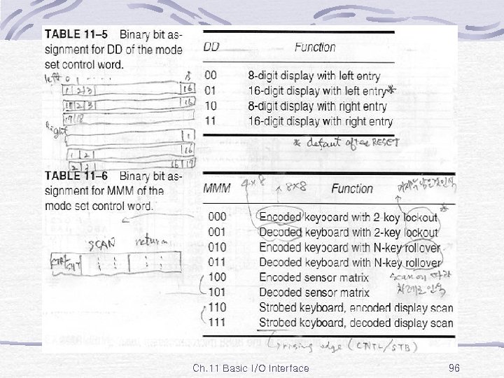
Table 11 -5 Ch. 11 Basic I/O Interface 96
8279 Control Word 2 -key lock-out : prevent two keys from being recognized if pressed simultaneously N-key rollover : accept all keys pressed simultaneously, from 1 st to last 001 PPPPP : clock command programmed internal clock divider PPPPP : prescaler that divide clock input pin(CLK) to achieve the desired operating frequency of approximately 100 KHz CLK=1 MHz : PPPPP=1010=010102, CLK=3 MHz : 30=111102 010 Z 0 AAA : read FIFO select address of a keystroke from internal FIFO buffer AAA : select desired FIFO location from 000 to 111 Ch. 11 Basic I/O Interface 97
8279 Control Word Z : auto-increment for address 011 Z AAAA : display read select read address of one of display RAM position AAAA : address of position to be read Z : auto-increment for address 100 Z AAAA : write display select write address of one of display A… : address position to be written to through data port 101 0 WW BB : display write inhibit writing to either half of each display RAM location left W : inhibit writing to leftmost 4 bits BB : blank(turn off) either half of output pins Ch. 11 Basic I/O Interface 98
8279 Control Word 110 0 CCFA : clear display, FIFO, or both display and FIFO(All) F : clear FIFO and display RAM status, set address pointer to 000 CC = 00 or 01 : all of display RAM ⇒ 00 H(0000) CC = 10 : 20 H(space, 0010 0000) CC = 11 : FFH(1111) 111 E 000 : end of interrupt to clear IRQ pin to zero in sensor matrix mode E=1 : used special error mode status reg. indicate if multiple key closure have occur Ch. 11 Basic I/O Interface 99
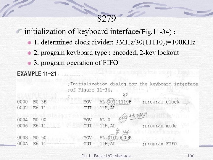
8279 initialization of keyboard interface(Fig. 11 -34) : 1. determined clock divider: 3 MHz/30(111102)=100 KHz 2. program keyboard type : encoded, 2 -key lockout 3. program operation of FIFO Ex. 11 -21 Ch. 11 Basic I/O Interface 100
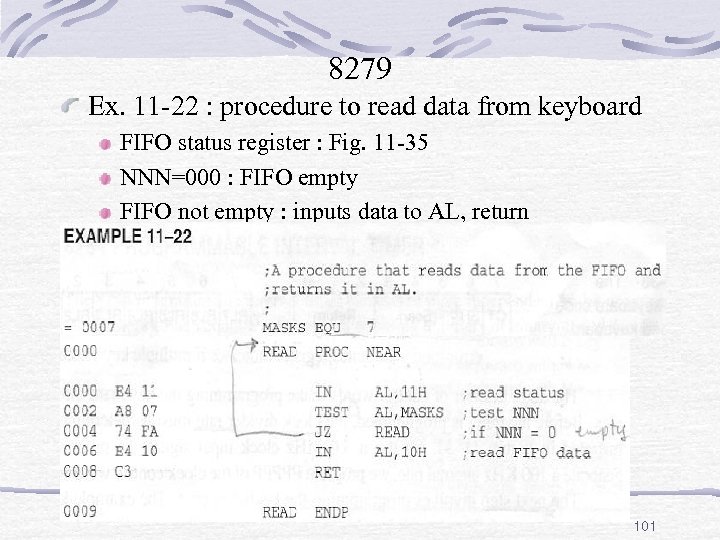
8279 Ex. 11 -22 : procedure to read data from keyboard FIFO status register : Fig. 11 -35 NNN=000 : FIFO empty FIFO not empty : inputs data to AL, return 101
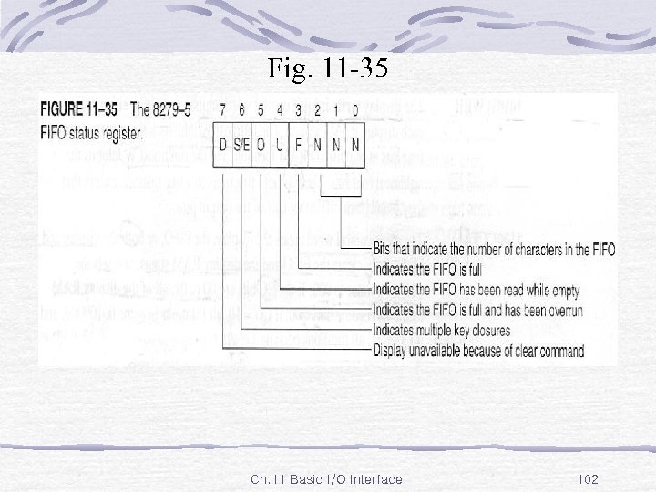
Fig. 11 -35 Ch. 11 Basic I/O Interface 102
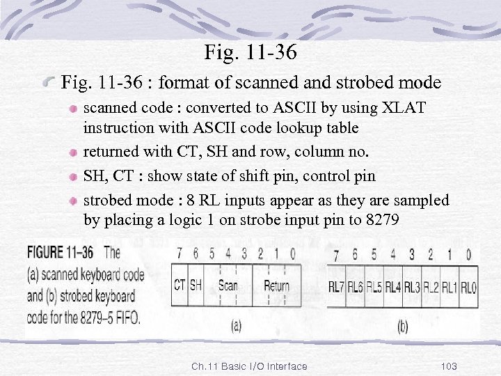
Fig. 11 -36 : format of scanned and strobed mode scanned code : converted to ASCII by using XLAT instruction with ASCII code lookup table returned with CT, SH and row, column no. SH, CT : show state of shift pin, control pin strobed mode : 8 RL inputs appear as they are sampled by placing a logic 1 on strobe input pin to 8279 Ch. 11 Basic I/O Interface 103
Six-Digit Display Interface Fig. 11 -37 : interfaced 6 -digit numeric display to 8088 PAL 16 L 8 : decoded 8279 at I/O port 20 H, 21 H segment data : supplied displays through OUTA, OUTB buffered by segment driver(ULN 2003 A) 3 -to-8 decoder(74 ALS 138) : enable anode switch (5 -0. 2 -1. 65 -0. 4)/60 m. A=2. 75/0. 06=45. 8 47Ω (5 -0. 7 -0. 4)/80 m. A/100=3. 9/0. 8 m. A=4. 875 K=4. 8 K Ex. 11 -23 : initialization Ex. 11 -24 : procedure for displaying data : transferred to procedure through AX AH : 7 -segment display code AL : address of displayed digit Ch. 11 Basic I/O Interface 104
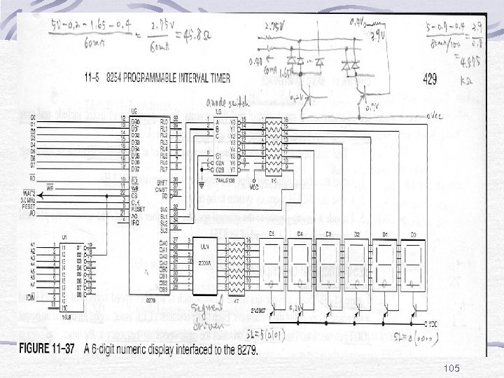
Fig. 11 -37 105
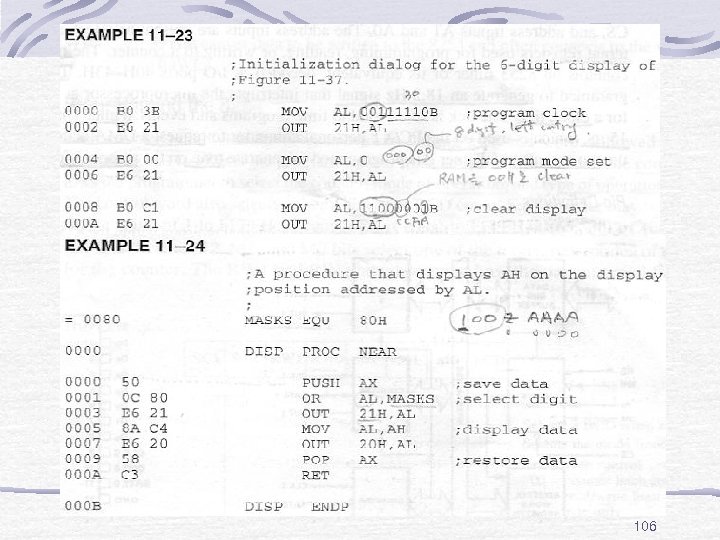
Ex. 11 -23, 24 106
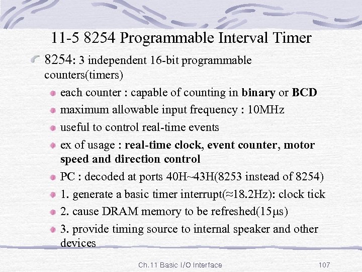
11 -5 8254 Programmable Interval Timer 8254: 3 independent 16 -bit programmable counters(timers) each counter : capable of counting in binary or BCD maximum allowable input frequency : 10 MHz useful to control real-time events ex of usage : real-time clock, event counter, motor speed and direction control PC : decoded at ports 40 H~43 H(8253 instead of 8254) 1. generate a basic timer interrupt(≈18. 2 Hz): clock tick 2. cause DRAM memory to be refreshed(15µs) 3. provide timing source to internal speaker and other devices Ch. 11 Basic I/O Interface 107
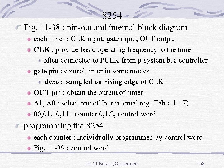
8254 Fig. 11 -38 : pin-out and internal block diagram each timer : CLK input, gate input, OUT output CLK : provide basic operating frequency to the timer often connected to PCLK from µ system bus controller gate pin : control timer in some modes always sampled on rising edge of CLK OUT pin : obtain the output of timer A 1, A 0 : select one of four internal reg. (Table 11 -7) 00, 01, 10, 11 : counter 0, 1, 2, control word programming the 8254 each counter : individually programmed by control word Fig. 11 -39 : control word Ch. 11 Basic I/O Interface 108
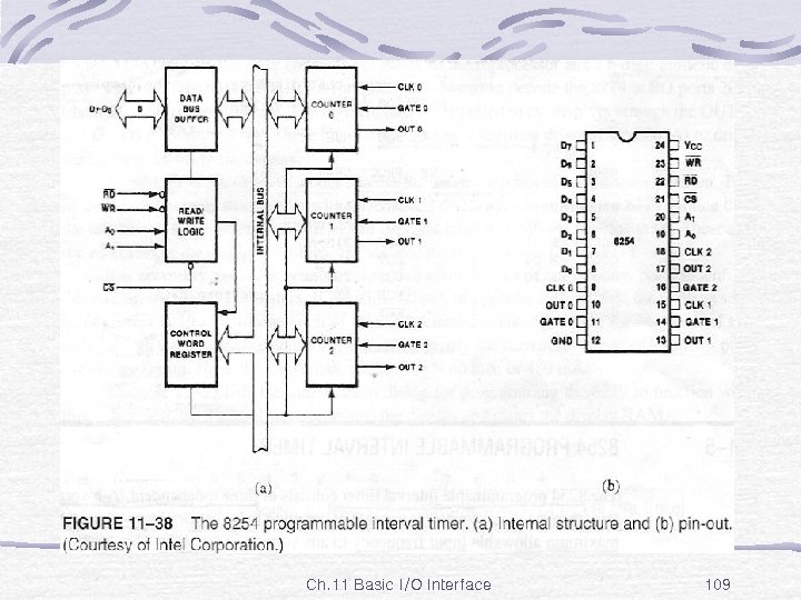
Fig. 11 -38 Ch. 11 Basic I/O Interface 109
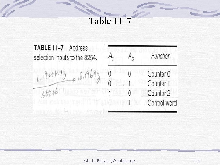
Table 11 -7 Ch. 11 Basic I/O Interface 110
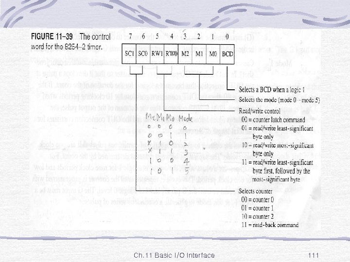
Fig. 11 -39 Ch. 11 Basic I/O Interface 111
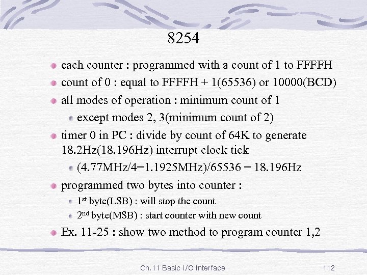
8254 each counter : programmed with a count of 1 to FFFFH count of 0 : equal to FFFFH + 1(65536) or 10000(BCD) all modes of operation : minimum count of 1 except modes 2, 3(minimum count of 2) timer 0 in PC : divide by count of 64 K to generate 18. 2 Hz(18. 196 Hz) interrupt clock tick (4. 77 MHz/4=1. 1925 MHz)/65536 = 18. 196 Hz programmed two bytes into counter : 1 st byte(LSB) : will stop the count 2 nd byte(MSB) : start counter with new count Ex. 11 -25 : show two method to program counter 1, 2 Ch. 11 Basic I/O Interface 112
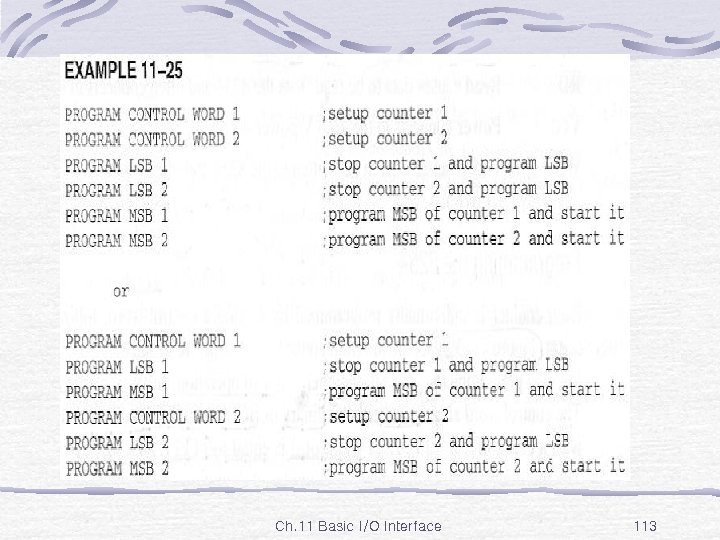
Ex. 11 -25 Ch. 11 Basic I/O Interface 113
Modes of operation Fig. 11 -40 : functions six modes with CLK, gate, OUT mode 0 : interrupt on terminal count typically used for event counting OUT = 0 : when control word is written and until counter reach zero G : no effected on OUT, =1: enable counting, =0: disable mode 1 : hardware retriggerable one-shot monostable multivibrator : one-shot pulse G : trigger, retrigger counter mode 2 : rate generator functions like a divide-by-N counter Ch. 11 Basic I/O Interface 114
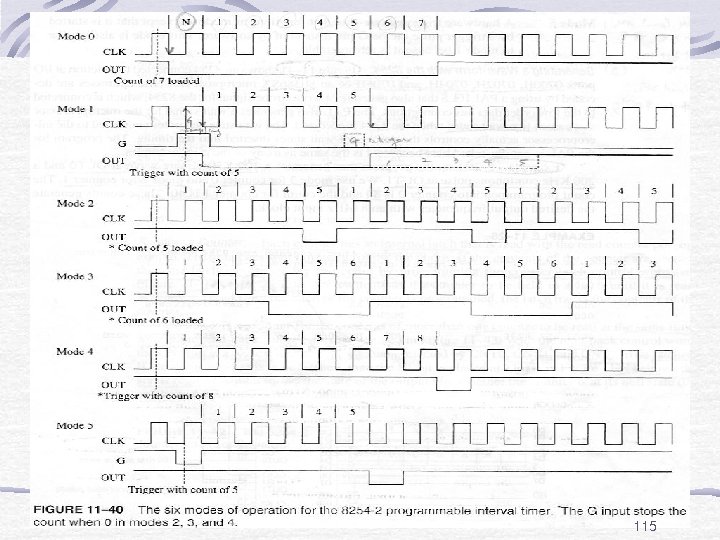
Fig. 11 -40 115
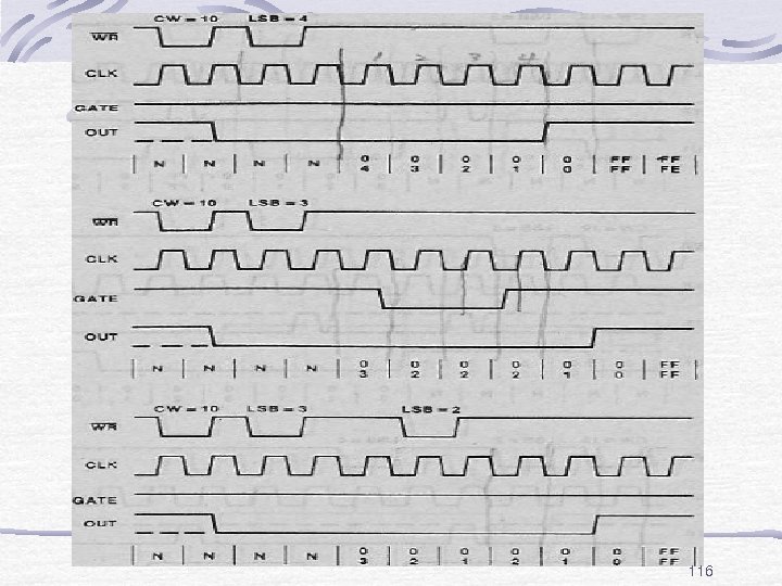
Fig. mode 0 116
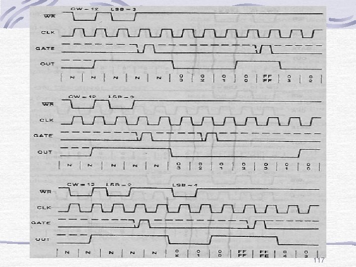
Fig. mode 1 117
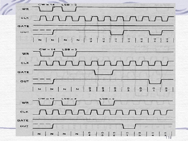
Fig. mode 2 118
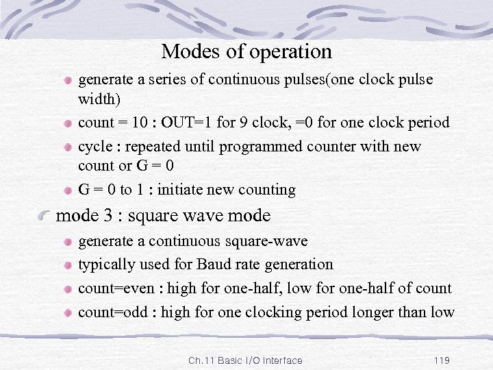
Modes of operation generate a series of continuous pulses(one clock pulse width) count = 10 : OUT=1 for 9 clock, =0 for one clock period cycle : repeated until programmed counter with new count or G = 0 to 1 : initiate new counting mode 3 : square wave mode generate a continuous square-wave typically used for Baud rate generation count=even : high for one-half, low for one-half of count=odd : high for one clocking period longer than low Ch. 11 Basic I/O Interface 119
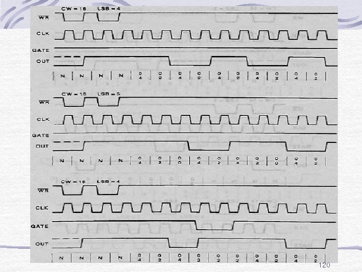
Fig. mode 3 120
Modes of operation mode 4 : software triggered strobe produce a single pulse at OUT count= 10 : OUT=1 for 10 clock, =0 for one clock period OUT : initially high G : no effected on OUT, =1: enable counting, =0: disable cycle : not begin until counter loaded new count mode 5 : hardware triggered strobe(retriggerable) like as mode 4, except that started by trigger pulse on G similar to mode 1 : retriggerable GATE operation : minimum, maximum initial count : Ch. 11 Basic I/O Interface 121
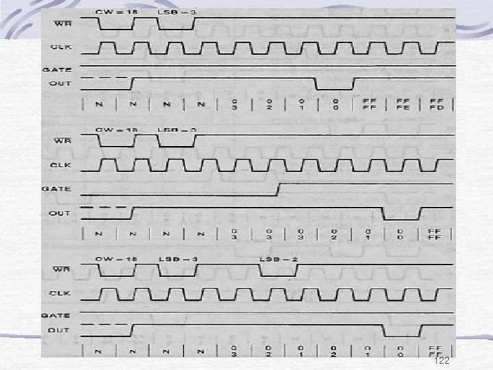
Fig. mode 4 122
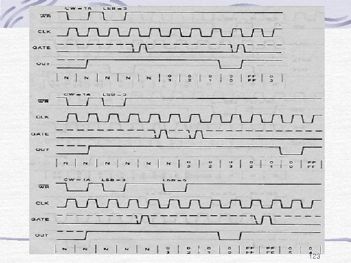
Fig. mode 5 123
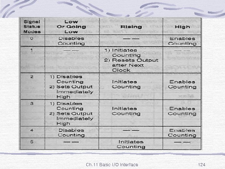
Fig. GATE operation Ch. 11 Basic I/O Interface 124
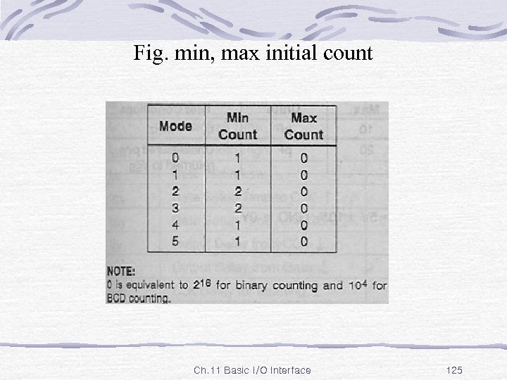
Fig. min, max initial count Ch. 11 Basic I/O Interface 125
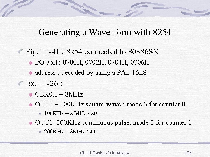
Generating a Wave-form with 8254 Fig. 11 -41 : 8254 connected to 80386 SX I/O port : 0700 H, 0702 H, 0704 H, 0706 H address : decoded by using a PAL 16 L 8 Ex. 11 -26 : CLK 0, 1 = 8 MHz OUT 0 = 100 KHz square-wave : mode 3 for counter 0 100 KHz = 8 MHz / 80 OUT 1=200 KHz continuous pulse: mode 2 for counter 1 200 KHz = 8 MHz / 40 Ch. 11 Basic I/O Interface 126
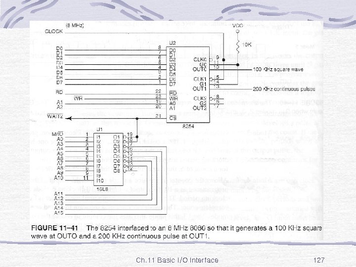
Fig. 11 -41 Ch. 11 Basic I/O Interface 127
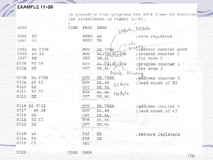
Ex. 11 -26 128
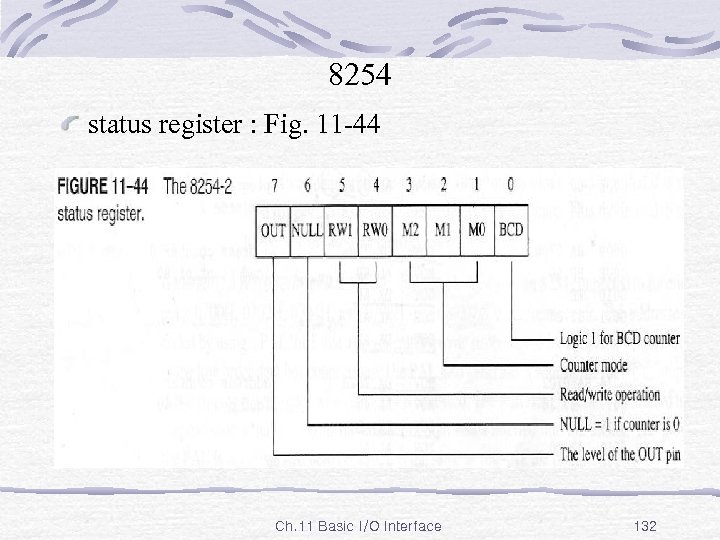
8254 Programmable Interval Timer Reading a Counter each counter : have an internal latch : normally follow the count can remember the count by programming the counter latch control word(Fig. 11 -42) held contents of counter until it is read-back control word(Fig. 11 -43) : read more than one counter at same time CNT’ = 0 : counters selected by CNT 0, CNT 1, CNT 2 ST’ =0 : latched status register Ch. 11 Basic I/O Interface 129
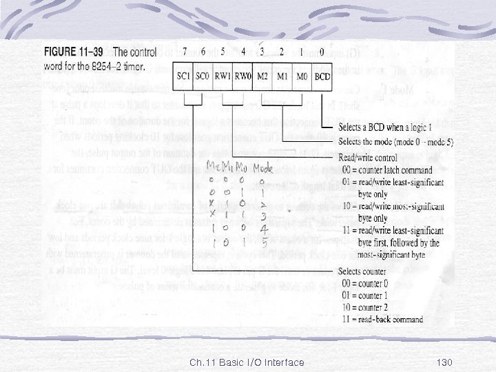
Fig. 11 -39 Ch. 11 Basic I/O Interface 130
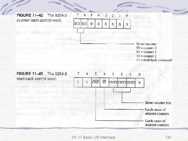
Fig. 11 -42, 43 Ch. 11 Basic I/O Interface 131
8254 status register : Fig. 11 -44 Ch. 11 Basic I/O Interface 132
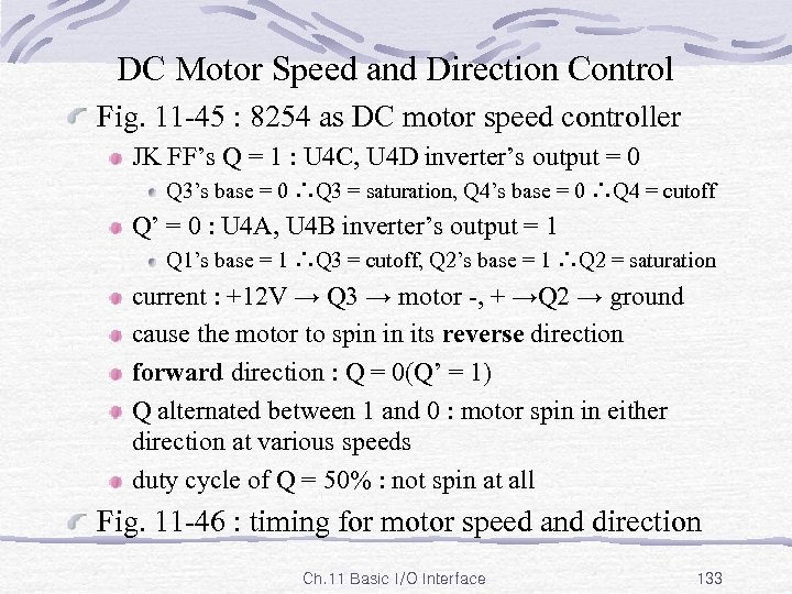
DC Motor Speed and Direction Control Fig. 11 -45 : 8254 as DC motor speed controller JK FF’s Q = 1 : U 4 C, U 4 D inverter’s output = 0 Q 3’s base = 0 ∴Q 3 = saturation, Q 4’s base = 0 ∴Q 4 = cutoff Q’ = 0 : U 4 A, U 4 B inverter’s output = 1 Q 1’s base = 1 ∴Q 3 = cutoff, Q 2’s base = 1 ∴Q 2 = saturation current : +12 V → Q 3 → motor -, + →Q 2 → ground cause the motor to spin in its reverse direction forward direction : Q = 0(Q’ = 1) Q alternated between 1 and 0 : motor spin in either direction at various speeds duty cycle of Q = 50% : not spin at all Fig. 11 -46 : timing for motor speed and direction Ch. 11 Basic I/O Interface 133
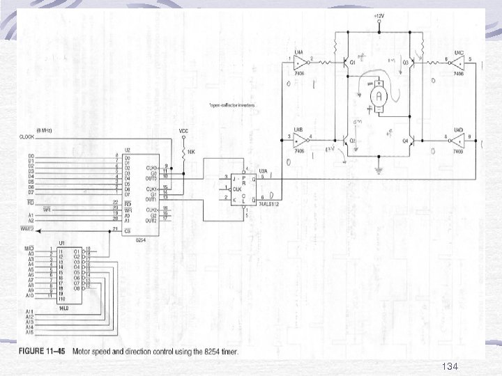
Fig. 11 -45 134
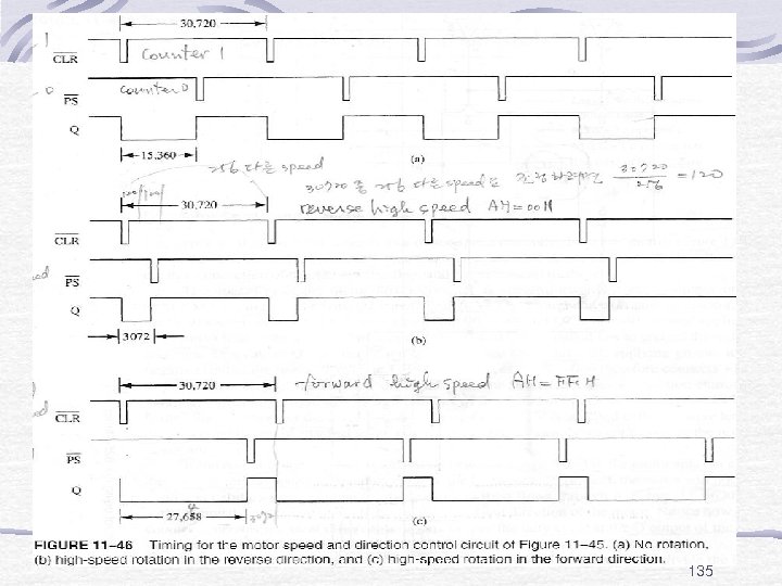
Fig. 11 -46 135
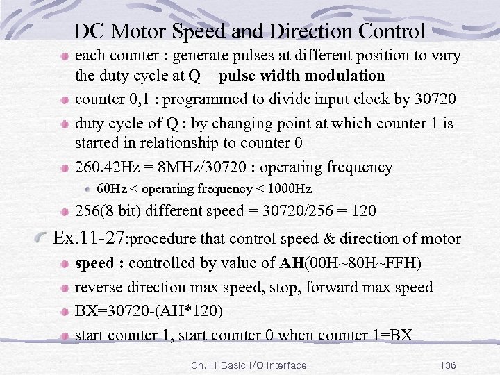
DC Motor Speed and Direction Control each counter : generate pulses at different position to vary the duty cycle at Q = pulse width modulation counter 0, 1 : programmed to divide input clock by 30720 duty cycle of Q : by changing point at which counter 1 is started in relationship to counter 0 260. 42 Hz = 8 MHz/30720 : operating frequency 60 Hz < operating frequency < 1000 Hz 256(8 bit) different speed = 30720/256 = 120 Ex. 11 -27: procedure that control speed & direction of motor speed : controlled by value of AH(00 H~80 H~FFH) reverse direction max speed, stop, forward max speed BX=30720 -(AH*120) start counter 1, start counter 0 when counter 1=BX Ch. 11 Basic I/O Interface 136
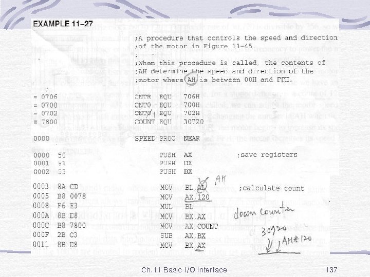
Ex. 11 -27 Ch. 11 Basic I/O Interface 137
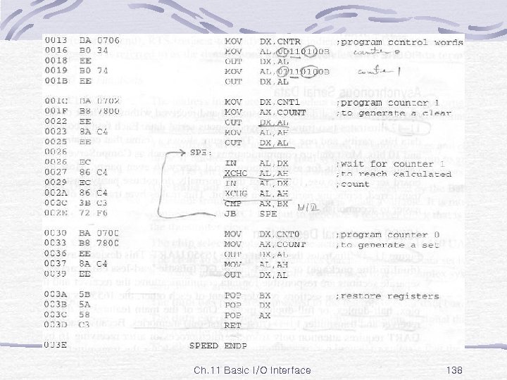
Ex. 11 -27 Ch. 11 Basic I/O Interface 138
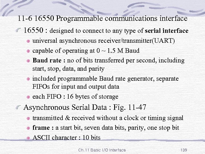
11 -6 16550 Programmable communications interface 16550 : designed to connect to any type of serial interface universal asynchronous receiver/transmitter(UART) capable of operating at 0 ~ 1. 5 M Baud rate : no of bits transferred per second, including start, stop, data, and parity included programmable Baud rate generator, separate FIFOs for input and output data each FIFO : 16 bytes of storage Asynchronous Serial Data : Fig. 11 -47 transmitted & received without a clock or timing signal frame : a start bit, seven data bits, parity, one stop bit ASCII character : 10 bits Ch. 11 Basic I/O Interface 139
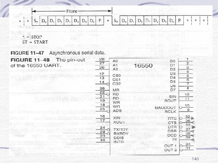
16550 Functional Description Fig. 11 -48 : pin-out of 16550 140
16550 Functional Description 40 -pin DIP(dual in-line package) : Fig 11 -48, 44 pin PLCC(plastic lead-less chip carrier) able function in simplex, half-duplex, full-duplex mode simplex : transmitter or receiver is used by itself such as FM(frequency modulation) radio station half-duplex : transmit and receive, but not both at same time such as CB(citizens band) radio full-duplex : allow transmit and receive in both directions simultaneously 16550 : control a modem(modulator/demodulator) convert TTL levels of serial data into audio tones that can pass through telephone system Ch. 11 Basic I/O Interface 141
16550 Functional Description six pin : devoted to modem control DSR’(data set ready) input : indicate that modem or data set is ready to operate DTR’(data terminal ready) output : indicate that data terminal(16550) is ready to function CTS’(clear-to-send) input : indicate that modem or data set is ready to exchange information. used in half-duplex RTS’(request-to-send) output : indicate that UART wish to send data RI’(ring indicator) input : by modem to indicate that telephone is ringing DCD’(data carrier detect) input : used by modem to signal the 16550 that a carrier is present Ch. 11 Basic I/O Interface 142
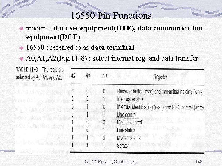
16550 Pin Functions modem : data set equipment(DTE), data communication equipment(DCE) 16550 : referred to as data terminal A 0, A 1, A 2(Fig. 11 -8) : select internal reg. and data transfer Ch. 11 Basic I/O Interface 143
16550 Pin Functions ADS’(address strobe) input : latch address lines and chip select lines CS 0, CS 1, CS 2’(chip select) : all active to enable 16550 D 7~D 0 : data bus BAUDOUT’ : clock signal generated by BAUD rate generator from transmitter section. connected to RCLK input to generate a receive clock RCLK(receiver clock) : clock to receiver section always 16 desired receiver Baud rate DDIS(disable driver) output : logic 0 to indicate that µ is reading data from UART can used to change direction of data flow through a buffer INTR(interrupt request) output : to µ Ch. 11 Basic I/O Interface 144
16550 Pin Functions MR(master reset) input : initialize 16550 connected to system RESET signal. interrupt disable RD, RD’ input(either) : cause data to be read from register specified by address input WR, WR’ input(either) : cause to transfer command data to 16550 SIN(serial input) : accept serial data SOUT(serial output) : transmit serial data RXRDY’(receiver ready) : used to transfer received data via DMA TXRDY’(transmitter ready) : used to transfer transmitter data via DMA XIN, XOUT : connected crystal, or external timing source Ch. 11 Basic I/O Interface 145
Programming the 16550 two part : initialization dialog, operation dialog initialization dialog : after HW/SW reset 1. programming line control register(A 2, A 1, A 0=011) 2. Baud rate generator(enable divisor latch : line control reg) divisor : LSB = 000, MSB = 001 (A 2, A 1, A 0) 3. enable FIFO(A 2, A 1, A 0=010) 1. line control register : Fig. 11 -49 select no of data bit, no of stop bit, parity I/O port : 011(A 2, A 1, A 0) Table 11 -9 : ST, P, PE bit SB(send break)=1 : break is transmitted from SOUT pin break : at least two frame of logic 0 data Ch. 11 Basic I/O Interface 146
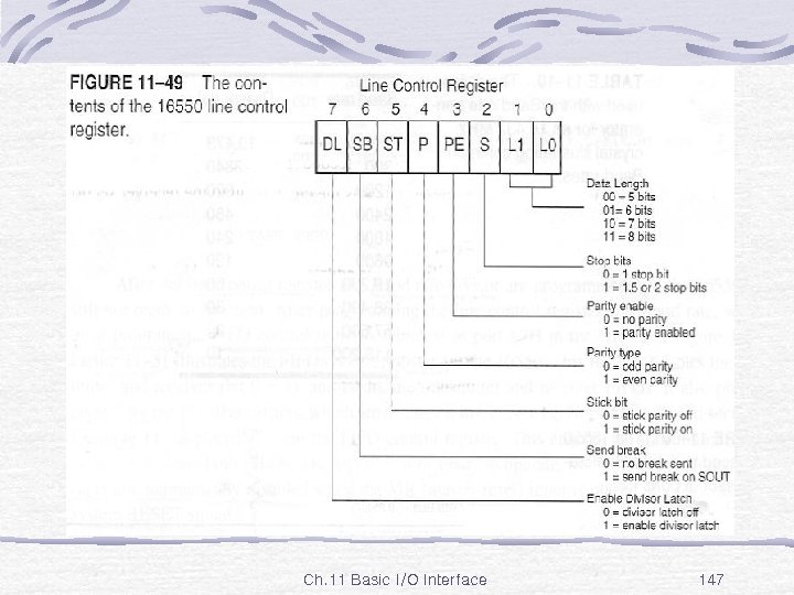
Fig. 11 -49 Ch. 11 Basic I/O Interface 147
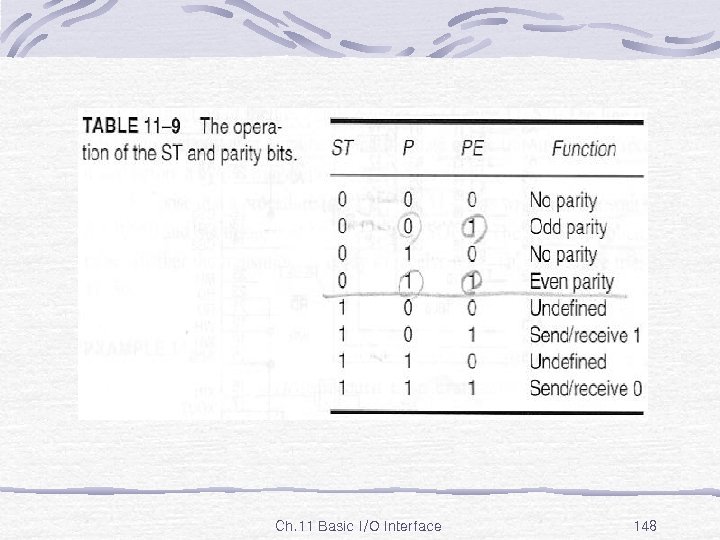
Table 11 -9 Ch. 11 Basic I/O Interface 148
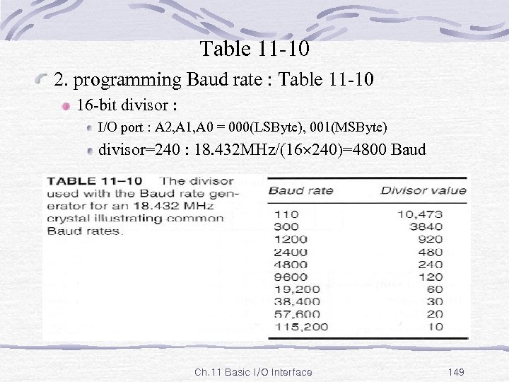
Table 11 -10 2. programming Baud rate : Table 11 -10 16 -bit divisor : I/O port : A 2, A 1, A 0 = 000(LSByte), 001(MSByte) divisor=240 : 18. 432 MHz/(16 240)=4800 Baud Ch. 11 Basic I/O Interface 149
Programming the 16550 Fig. 11 -50 : interface 16550 to 8088 using PAL 16 L 8 to decode F 0 H~F 7 H Ex. 11 -28 : asynchronous system required 7 data bits, odd parity, Baud rate of 9600 FIFO control register : Fig. 11 -51 I/O port = 010 (Table 11. 8) line status register(I/O port=101) : Fig. 11 -52 error condition, state of transmitter and receiver Sending Serial Data : Ex. 11 -29 transmit the contents of AH polled TH bit Ch. 11 Basic I/O Interface 150
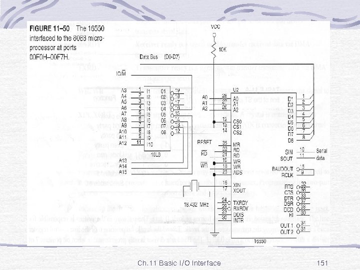
Fig. 11 -50 Ch. 11 Basic I/O Interface 151
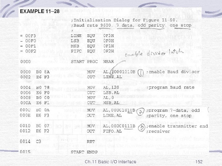
Ex. 11 -28 Ch. 11 Basic I/O Interface 152
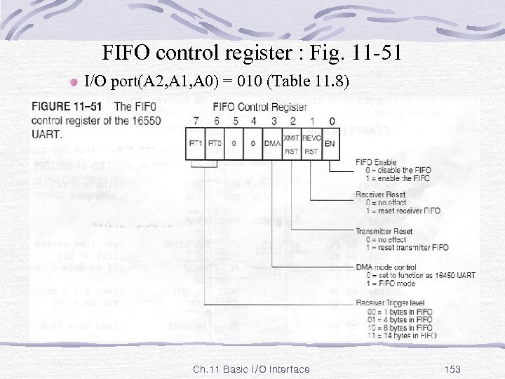
FIFO control register : Fig. 11 -51 I/O port(A 2, A 1, A 0) = 010 (Table 11. 8) Ch. 11 Basic I/O Interface 153
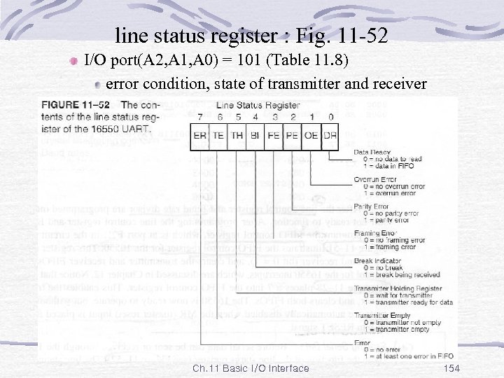
line status register : Fig. 11 -52 I/O port(A 2, A 1, A 0) = 101 (Table 11. 8) error condition, state of transmitter and receiver Ch. 11 Basic I/O Interface 154
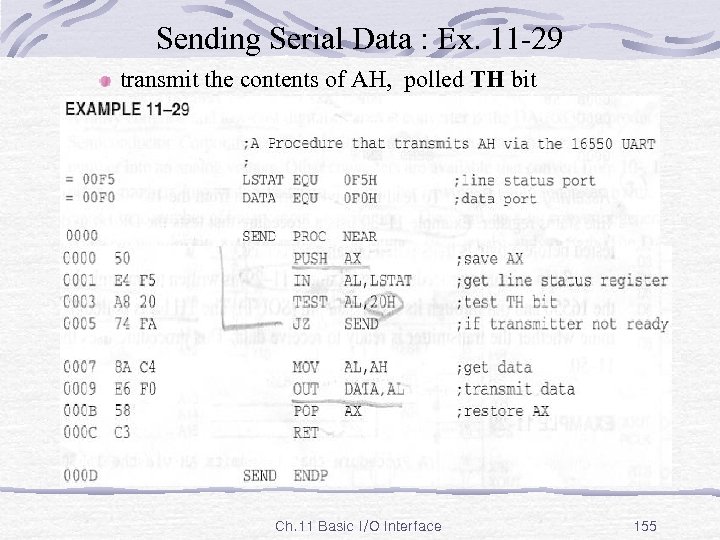
Sending Serial Data : Ex. 11 -29 transmit the contents of AH, polled TH bit Ch. 11 Basic I/O Interface 155
Programming the 16550 Receiving Serial Data : Ex. 11 -30 test DR bit return with AL(ASCII ‘? ’) : if detected error UART Errors : occur during normal operation parity error : indicate the received data with wrong parity encountered noise during reception framing error : start, stop bits are not in proper places received data at an incorrect Baud rate overrun error : data have overrun the internal receiver FIFO buffer only if s/w fail to read data from UART before FIFO is full BI(break indicator) bit : not checked break : two consecutive frame of logic 0 s on SIN pin of UART Ch. 11 Basic I/O Interface 156
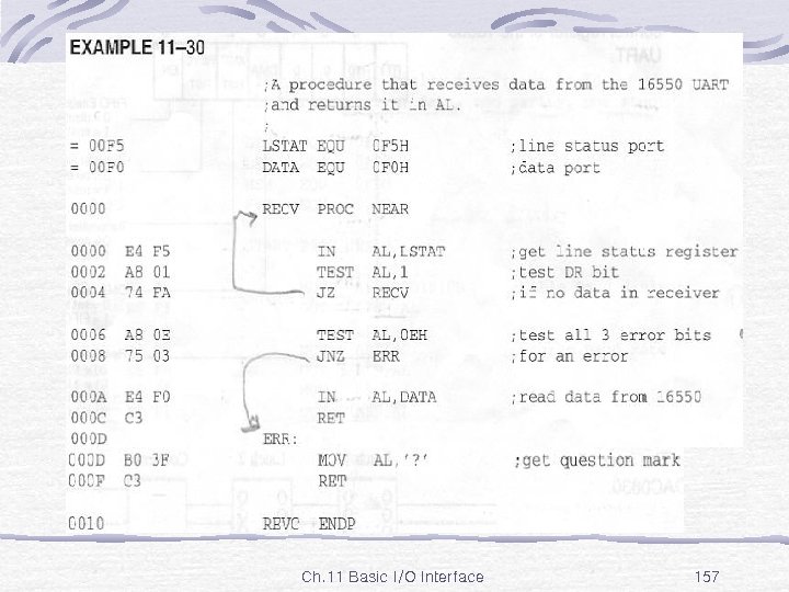
Ex. 11 -30 Ch. 11 Basic I/O Interface 157
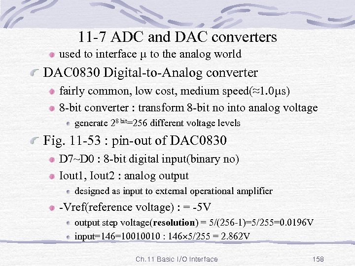
11 -7 ADC and DAC converters used to interface µ to the analog world DAC 0830 Digital-to-Analog converter fairly common, low cost, medium speed(≈1. 0µs) 8 -bit converter : transform 8 -bit no into analog voltage generate 28 bit=256 different voltage levels Fig. 11 -53 : pin-out of DAC 0830 D 7~D 0 : 8 -bit digital input(binary no) Iout 1, Iout 2 : analog output designed as input to external operational amplifier -Vref(reference voltage) : = -5 V output step voltage(resolution) = 5/(256 -1)=5/255=0. 0196 V input=146=10010010 : 146 5/255 = 2. 862 V Ch. 11 Basic I/O Interface 158
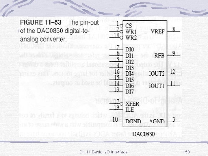
Fig. 11 -53 Ch. 11 Basic I/O Interface 159
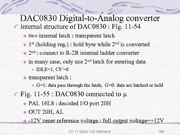
DAC 0830 Digital-to-Analog converter internal structure of DAC 0830 : Fig. 11 -54 two internal latch : transparent latch 1 st (holding reg. ) : hold byte while 2 nd is converted 2 nd : connect to R-2 R internal ladder converter in many case, only use 2 nd latch for entering data IDLE=1, CS’=0 transparent latch : G=1: data pass through the latch, G=0: data are latched or held Fig. 11 -55 : DAC 0830 connected to µ PAL 16 L 8 : decoded I/O port 20 H OUT 20 H, AL -12 V zener reference voltage : full output voltage=+12 V Ch. 11 Basic I/O Interface 160
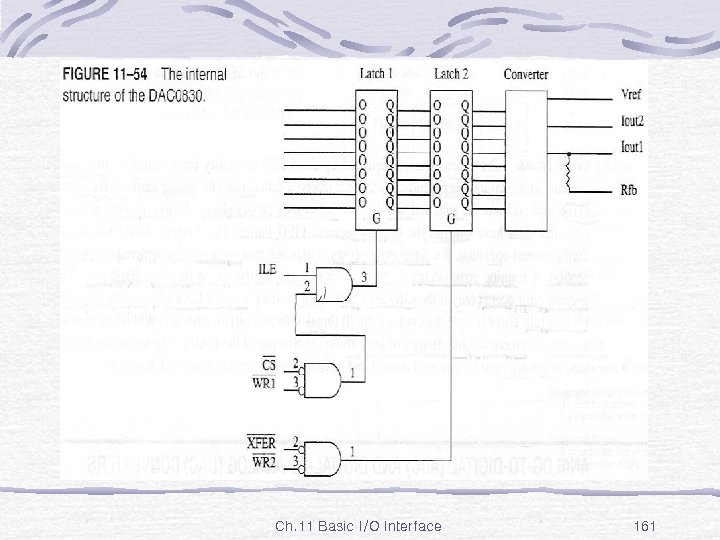
Fig. 11 -54 Ch. 11 Basic I/O Interface 161
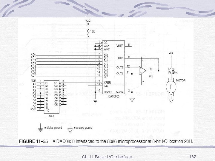
Fig. 11 -55 Ch. 11 Basic I/O Interface 162
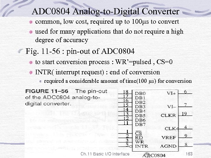
ADC 0804 Analog-to-Digital Converter common, low cost, required up to 100µs to convert used for many applications that do not require a high degree of accuracy Fig. 11 -56 : pin-out of ADC 0804 to start conversion process : WR’=pulsed , CS=0 INTR( interrupt request) : end of conversion required a considerable amount of time(100 µs) for conversion Ch. 11 Basic I/O Interface 163
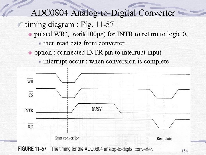
ADC 0804 Analog-to-Digital Converter timing diagram : Fig. 11 -57 pulsed WR’, wait(100µs) for INTR to return to logic 0, then read data from converter option : connected INTR pin to interrupt input interrupt occur : when conversion is complete 164
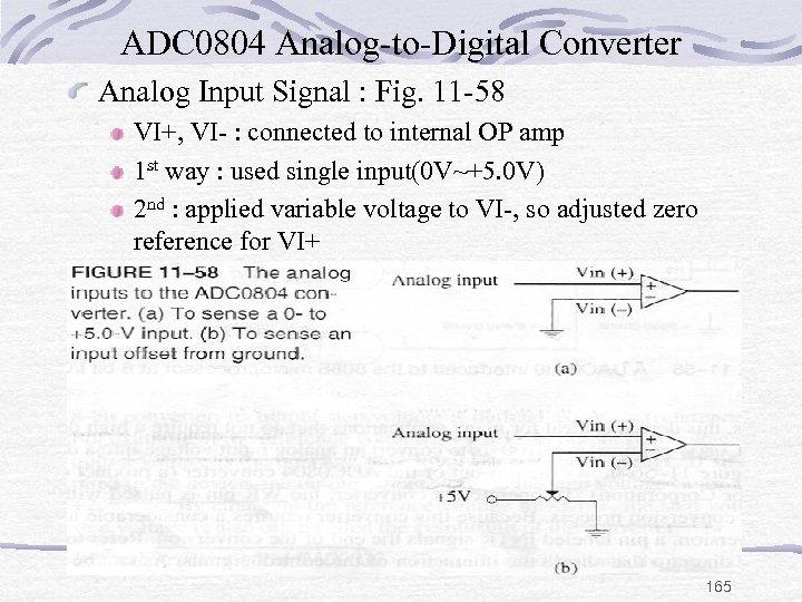
ADC 0804 Analog-to-Digital Converter Analog Input Signal : Fig. 11 -58 VI+, VI- : connected to internal OP amp 1 st way : used single input(0 V~+5. 0 V) 2 nd : applied variable voltage to VI-, so adjusted zero reference for VI+ 165
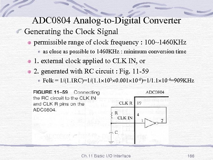
ADC 0804 Analog-to-Digital Converter Generating the Clock Signal permissible range of clock frequency : 100~1460 KHz as close as possible to 1460 KHz : minimum conversion time 1. external clock applied to CLK IN, or 2. generated with RC circuit : Fig. 11 -59 Fclk = 1/(1. 1 RC)=1/(1. 1 103 0. 001 10 -6)=1/1. 1 10 -6=909 KHz Ch. 11 Basic I/O Interface 166
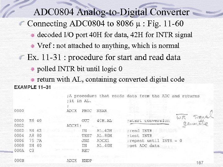
ADC 0804 Analog-to-Digital Converter Connecting ADC 0804 to 8086 µ : Fig. 11 -60 decoded I/O port 40 H for data, 42 H for INTR signal Vref : not attached to anything, which is normal Ex. 11 -31 : procedure for start and read data polled INTR bit until logic 0 return with AL, containing converted digital code 167
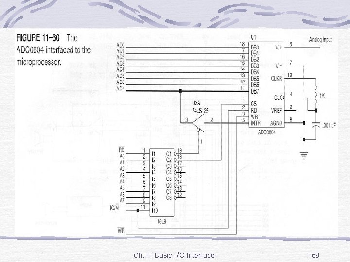
Fig. 11 -60 Ch. 11 Basic I/O Interface 168
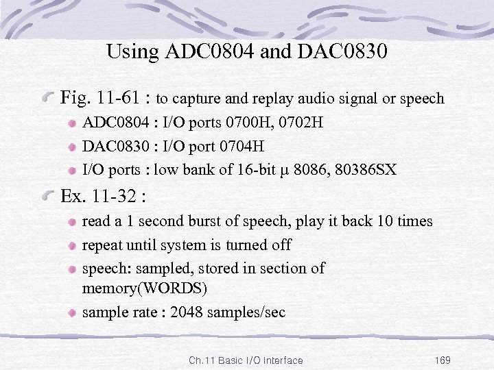
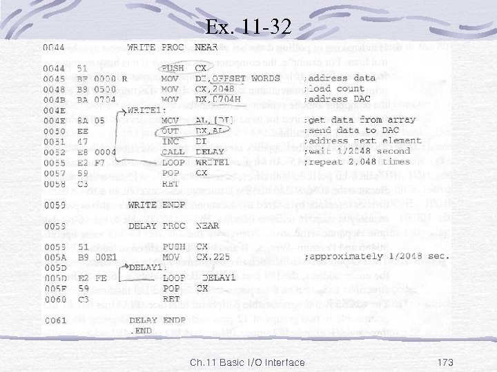
Using ADC 0804 and DAC 0830 Fig. 11 -61 : to capture and replay audio signal or speech ADC 0804 : I/O ports 0700 H, 0702 H DAC 0830 : I/O port 0704 H I/O ports : low bank of 16 -bit µ 8086, 80386 SX Ex. 11 -32 : read a 1 second burst of speech, play it back 10 times repeat until system is turned off speech: sampled, stored in section of memory(WORDS) sample rate : 2048 samples/sec Ch. 11 Basic I/O Interface 169
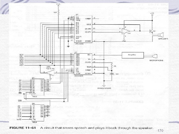
Fig. 11 -61 170
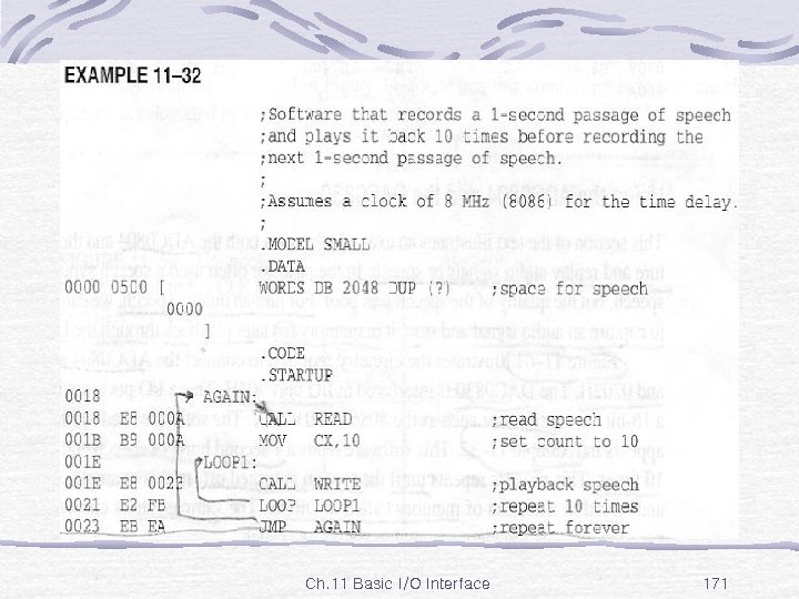
Ex. 11 -32 Ch. 11 Basic I/O Interface 171
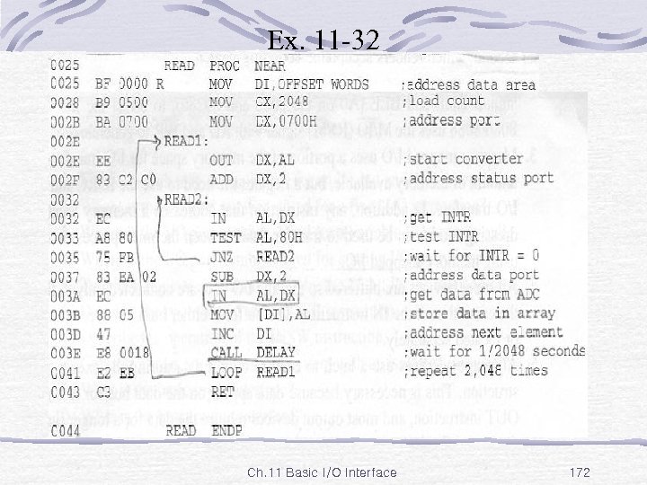
Ex. 11 -32 Ch. 11 Basic I/O Interface 172
Ex. 11 -32 Ch. 11 Basic I/O Interface 173
551c6877910bf6163130b7115879e1df.ppt