f65954022d952d547d06357a9dde300e.ppt
- Количество слайдов: 27
 Channel Width Reduction Techniques for System-on-Chip Circuits in Field-Programmable Gate Arrays Marvin Tom University of British Columbia Department of Electrical and Computer Engineering Vancouver, BC, Canada
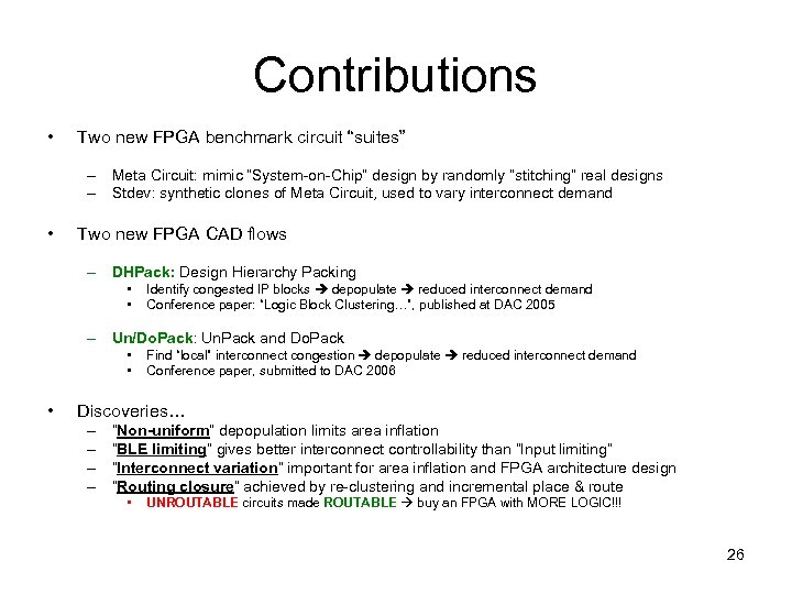
 Contributions • Two new FPGA benchmark circuit “suites” – Meta Circuit: mimic “System-on-Chip” design by randomly “stitching” real designs – Stdev: synthetic clones of Meta Circuit, used to vary interconnect demand • Two new FPGA CAD flows – DHPack: Design Hierarchy Packing • • Identify congested IP blocks depopulate reduced interconnect demand Conference paper: “Logic Block Clustering…”, published at DAC 2005 – Un/Do. Pack: Un. Pack and Do. Pack • • • Find “local” interconnect congestion depopulate reduced interconnect demand Conference paper, submitted to DAC 2006 Discoveries… – – “Non-uniform” depopulation limits area inflation “BLE limiting” gives better interconnect controllability than “Input limiting” “Interconnect variation” important for area inflation and FPGA architecture design “Routing closure” achieved by re-clustering and incremental place & route • UNROUTABLE circuits made ROUTABLE buy an FPGA with MORE LOGIC!!! 2
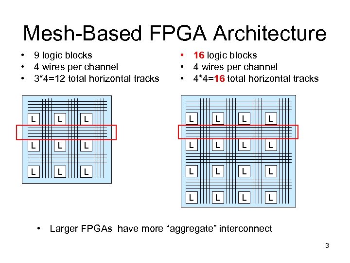 Mesh-Based FPGA Architecture • 9 logic blocks • 4 wires per channel • 3*4=12 total horizontal tracks • 16 logic blocks • 4 wires per channel • 4*4=16 total horizontal tracks L L L L L L L • Larger FPGAs have more “aggregate” interconnect 3
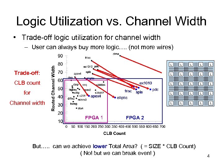 Logic Utilization vs. Channel Width • Trade-off logic utilization for channel width – User can always buy more logic…. (not more wires) L L L L Trade-off: L L L L CLB count L L L L L for L L L L L Channel width L L L FPGA 1 FPGA 2 But…. . can we achieve lower Total Area? ( = SIZE * CLB Count) ( No! but we can break even! ) 4
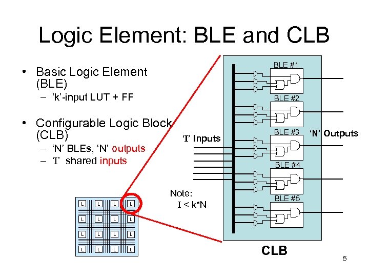 Logic Element: BLE and CLB BLE #1 • Basic Logic Element (BLE) – ‘k’-input LUT + FF BLE #2 • Configurable Logic Block (CLB) – ‘N’ BLEs, ‘N’ outputs – ‘I’ shared inputs L L L ‘N’ Outputs BLE #4 Note: I < k*N BLE #5 L L BLE #3 L L ‘I’ Inputs CLB 5
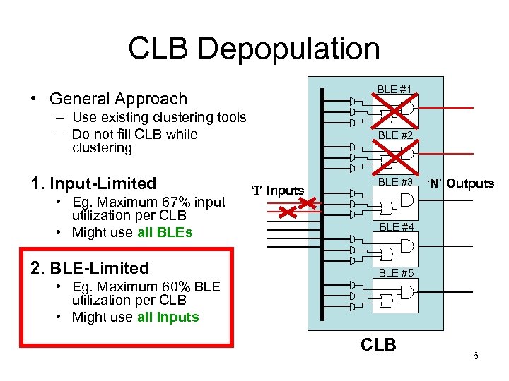 CLB Depopulation BLE #1 • General Approach – Use existing clustering tools – Do not fill CLB while clustering 1. Input-Limited • Eg. Maximum 67% input utilization per CLB • Might use all BLEs 2. BLE-Limited • Eg. Maximum 60% BLE utilization per CLB • Might use all Inputs BLE #2 ‘I’ Inputs BLE #3 ‘N’ Outputs BLE #4 BLE #5 CLB 6
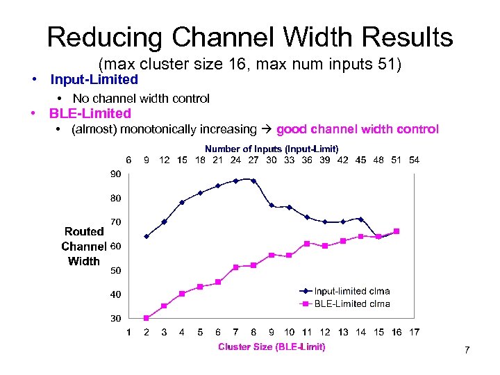 Reducing Channel Width Results (max cluster size 16, max num inputs 51) • Input-Limited • No channel width control • BLE-Limited • (almost) monotonically increasing good channel width control 7
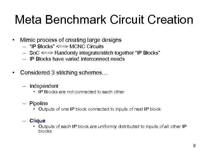 Meta Benchmark Circuit Creation • Mimic process of creating large designs – “IP Blocks” <==> MCNC Circuits – So. C <==> Randomly integrate/stitch together “IP Blocks” – IP Blocks have varied interconnect needs • Considered 3 stitching schemes… – Independent • IP Blocks are not connected to each other – Pipeline • Outputs of one IP block connected to inputs of next IP block – Clique • Outputs of each IP block are uniformly distributed to inputs of all other IP blocks 8
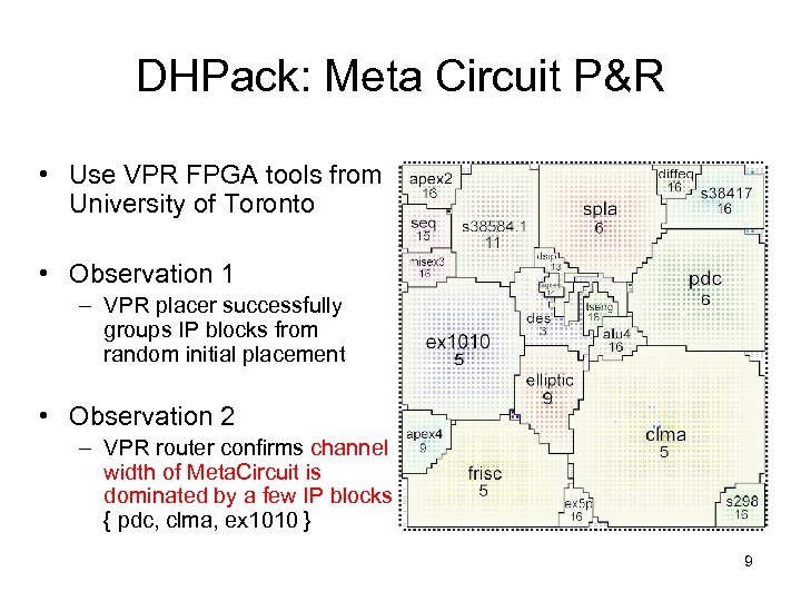 DHPack: Meta Circuit P&R • Use VPR FPGA tools from University of Toronto • Observation 1 – VPR placer successfully groups IP blocks from random initial placement • Observation 2 – VPR router confirms channel width of Meta. Circuit is dominated by a few IP blocks { pdc, clma, ex 1010 } 9
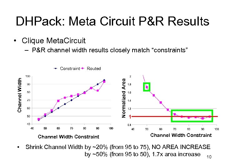 DHPack: Meta Circuit P&R Results • Clique Meta. Circuit – P&R channel width results closely match “constraints” Routed Normalized Area Channel Width Constraint • 1 Channel Width Constraint Shrink Channel Width by ~20% (from 95 to 75), NO AREA INCREASE by ~50% (from 95 to 50), 1. 7 x area increase 10
 Meta Circuits vs. Stdev Circuits • Meta Circuit Drawbacks – Design hierarchy boundaries not well-defined – Coarse-grained IP block boundary – Stitching unrealistic • Flip Flop placed at every output • Connections only have FO 1 • Stdev Circuits (created using GNL) – Synthetic clone of Meta circuits – Hierarchical specify Rent parameter of each partition • Root # I/Os, # IP blocks • Second Level 20 IP blocks, # LEs, Rent parameter 11
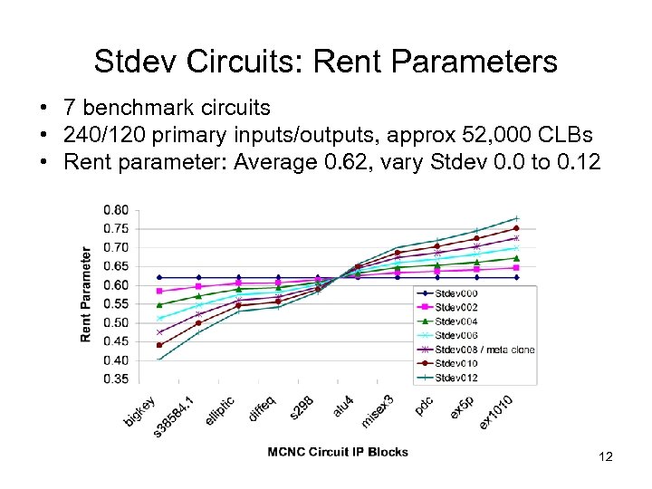 Stdev Circuits: Rent Parameters • 7 benchmark circuits • 240/120 primary inputs/outputs, approx 52, 000 CLBs • Rent parameter: Average 0. 62, vary Stdev 0. 0 to 0. 12 12
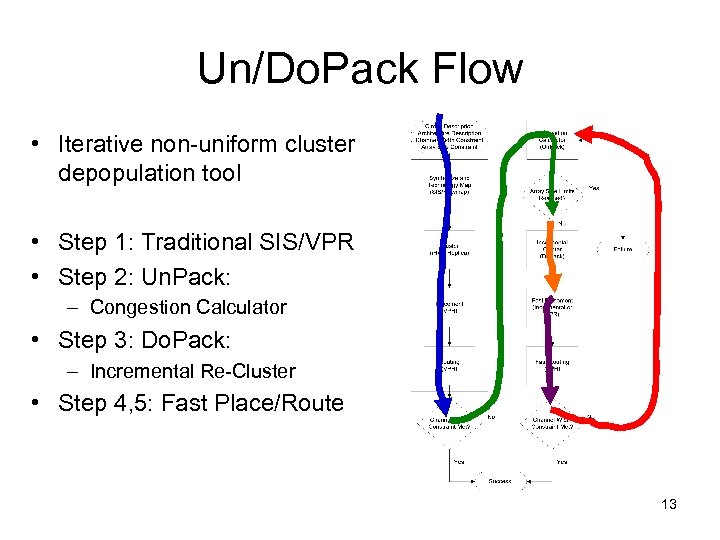 Un/Do. Pack Flow • Iterative non-uniform cluster depopulation tool • Step 1: Traditional SIS/VPR • Step 2: Un. Pack: – Congestion Calculator • Step 3: Do. Pack: – Incremental Re-Cluster • Step 4, 5: Fast Place/Route 13
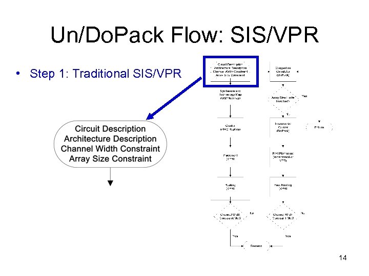 Un/Do. Pack Flow: SIS/VPR • Step 1: Traditional SIS/VPR 14
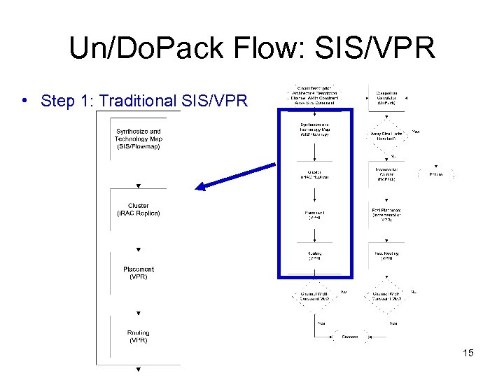 Un/Do. Pack Flow: SIS/VPR • Step 1: Traditional SIS/VPR 15
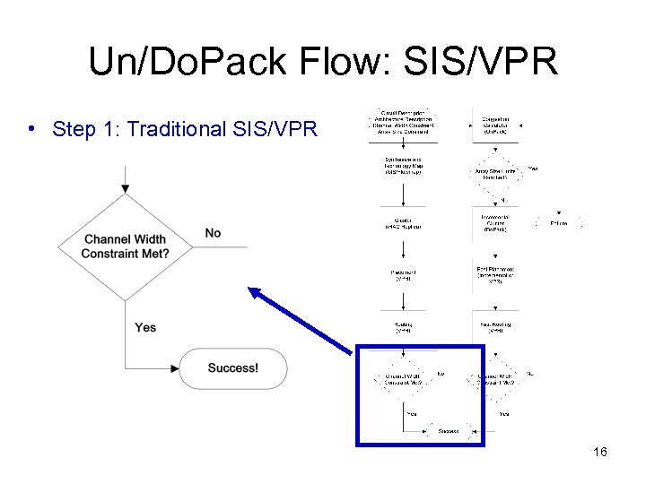 Un/Do. Pack Flow: SIS/VPR • Step 1: Traditional SIS/VPR 16
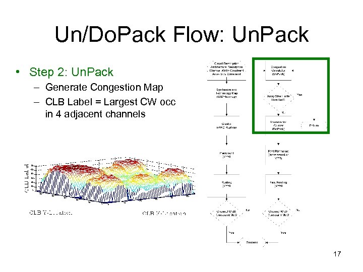 Un/Do. Pack Flow: Un. Pack • Step 2: Un. Pack – Generate Congestion Map – CLB Label = Largest CW occ in 4 adjacent channels 17
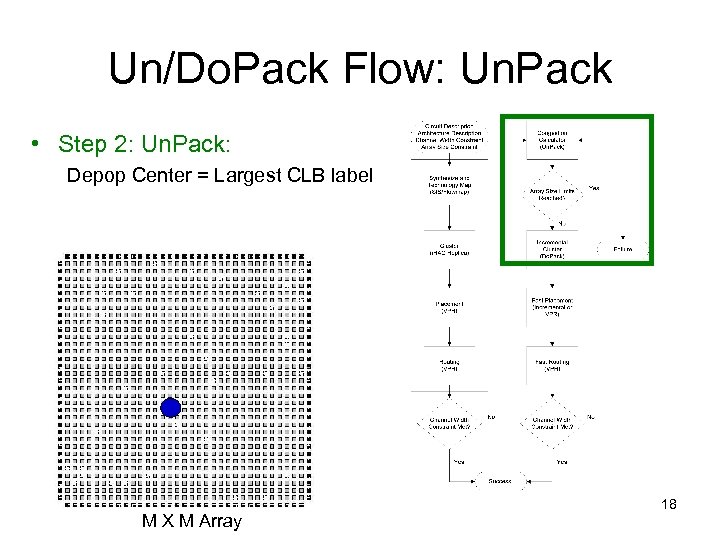 Un/Do. Pack Flow: Un. Pack • Step 2: Un. Pack: Depop Center = Largest CLB label M X M Array 18
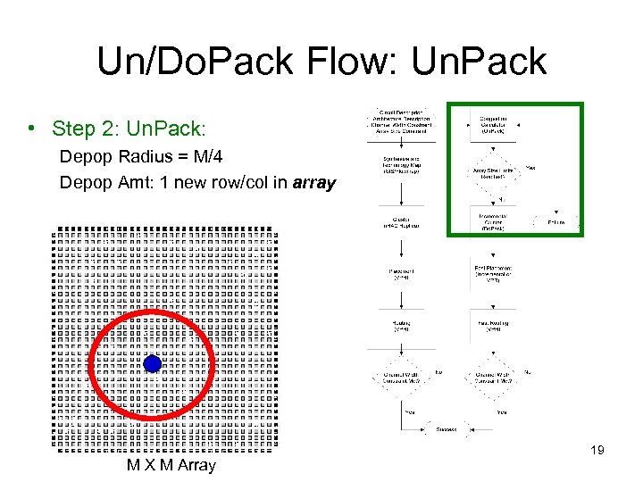 Un/Do. Pack Flow: Un. Pack • Step 2: Un. Pack: Depop Radius = M/4 Depop Amt: 1 new row/col in array M X M Array 19
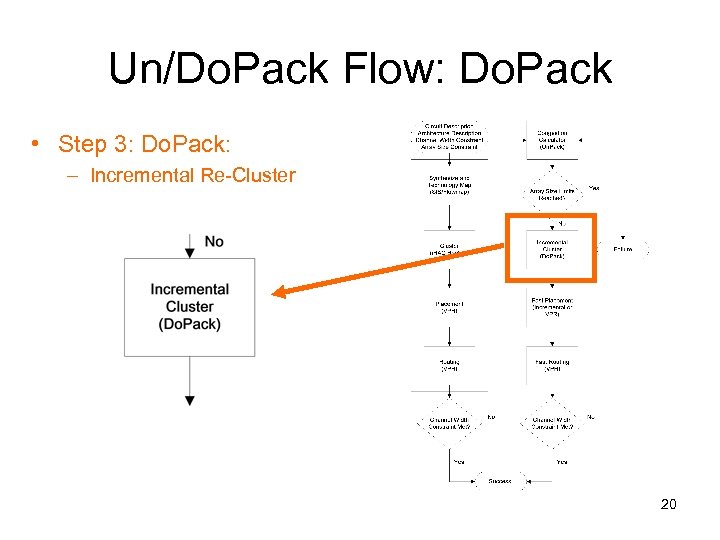 Un/Do. Pack Flow: Do. Pack • Step 3: Do. Pack: – Incremental Re-Cluster 20
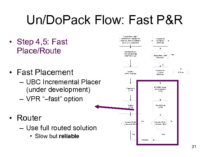 Un/Do. Pack Flow: Fast P&R • Step 4, 5: Fast Place/Route • Fast Placement – UBC Incremental Placer (under development) – VPR “–fast” option • Router – Use full routed solution • Slow but reliable 21
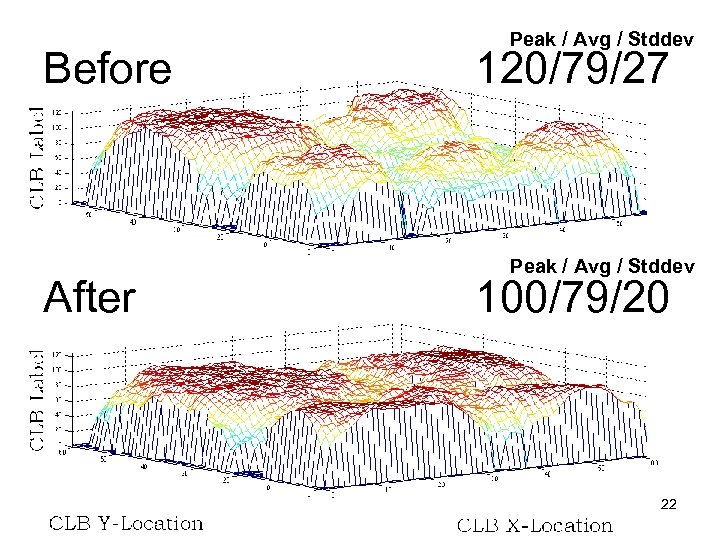 Before After Peak / Avg / Stddev 120/79/27 Peak / Avg / Stddev 100/79/20 22
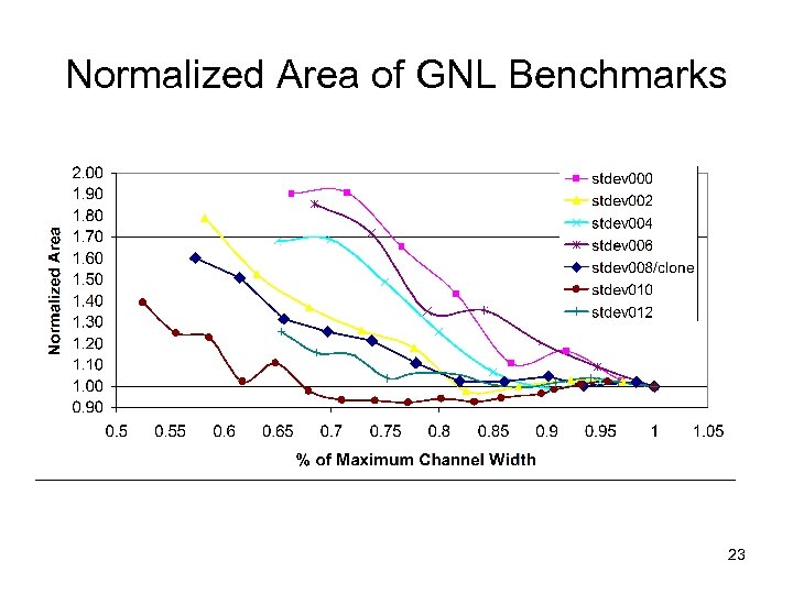 Normalized Area of GNL Benchmarks 23
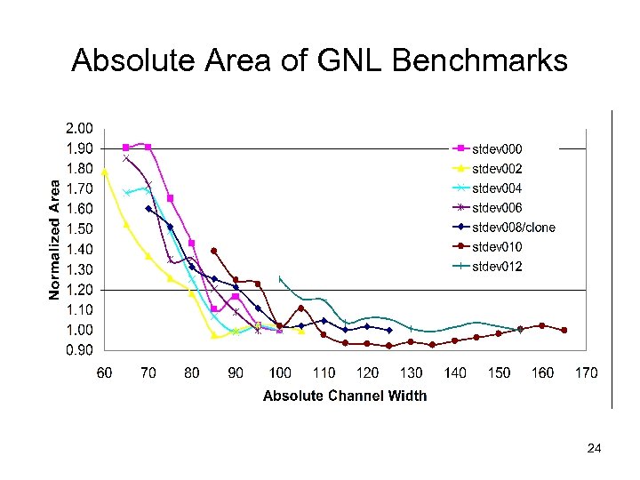 Absolute Area of GNL Benchmarks 24
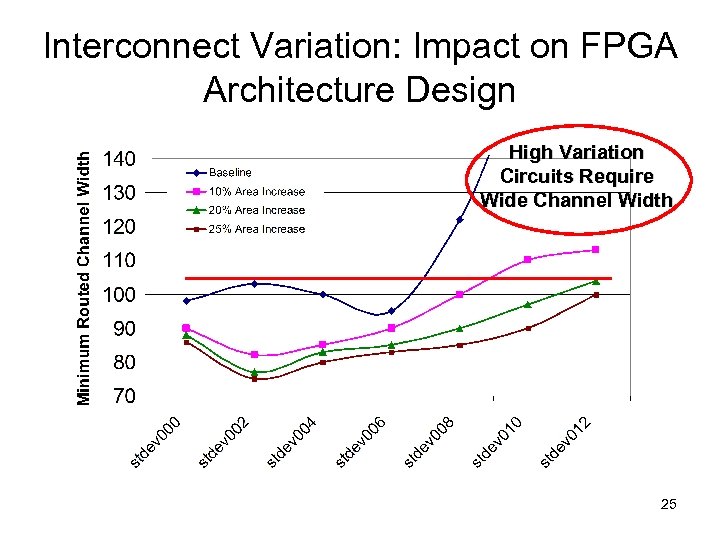 Interconnect Variation: Impact on FPGA Architecture Design High Variation Circuits Require Wide Channel Width 25
 Contributions • Two new FPGA benchmark circuit “suites” – Meta Circuit: mimic “System-on-Chip” design by randomly “stitching” real designs – Stdev: synthetic clones of Meta Circuit, used to vary interconnect demand • Two new FPGA CAD flows – DHPack: Design Hierarchy Packing • • Identify congested IP blocks depopulate reduced interconnect demand Conference paper: “Logic Block Clustering…”, published at DAC 2005 – Un/Do. Pack: Un. Pack and Do. Pack • • • Find “local” interconnect congestion depopulate reduced interconnect demand Conference paper, submitted to DAC 2006 Discoveries… – – “Non-uniform” depopulation limits area inflation “BLE limiting” gives better interconnect controllability than “Input limiting” “Interconnect variation” important for area inflation and FPGA architecture design “Routing closure” achieved by re-clustering and incremental place & route • UNROUTABLE circuits made ROUTABLE buy an FPGA with MORE LOGIC!!! 26
 End of Talk


