959681e8fbc9d2c473eb424709b3c7dc.ppt
- Количество слайдов: 36
 CEG 790 Synthesis and Optimization of Digital Circuits Dr. Travis Doom Wright State University Computer Science and Engineering
 CEG 790 Outline n Introduction – – – n Techniques for Digital Synthesis – – – n Architectural-Level Synthesis Logic-Level Synthesis Geometric Synthesis Techniques for Formal Verification – – n Microelectronics Micro “economics” What is “design”? Automated Theorem-Provers Graph-based Algorithms Reengineering
 CEG 790 Overview: Microelectronics n What is a microelectronic component? – – Constructed by patterning a substrate and locally modifying its properties to shape “wires” and logical “devices” – Complex functions are “integrated” into one physical package – n Devices which exploit the properties of semiconductor materials Fabrication is very complex Microelectronic components enable “smart” systems – Prevalent in modern systems – Failures are not taken well - most applications are “critical”
 CEG 790 Overview: “Micro” Economics n IC technology has progressed tremendously over 40 yrs. – n Moore’s Law [SSI - ‘ 60, MSI - ‘ 70, VLSI - ‘ 90, ? ? - ‘ 00] Costs have increased tremendously as well – Larger capital investment due to cost of refining precision – Larger scale increases effort to achieve zero-defect design l l – ICs are nearly impossible to repair The design must be correct (and manufacturing defects limited) Design and manufacturing costs must be recovered via sales l l l Few designs do enjoy a high volume of sales or long life Many systems require specialized devices (ASICs) - few hold a significant market share individually Improvement of technology causes immediate obsolescence
 CEG 790 Overview: “Micro” Economics n How can costs be reduced and net profit increased? – Minimize Design (and test) time l – n Reduces both time-to-market and designers’ salaries Increase quality of design to increase fabrication yield and provide competitive performance Design automation techniques provide an effective means for designing economically viable products – Carrying out a full design w/o errors is increasingly difficult w/o systematic techniques to handle data – CAD techniques tend to focus on Digital Synchronous circuits as they represent the vast majority of circuits in the market
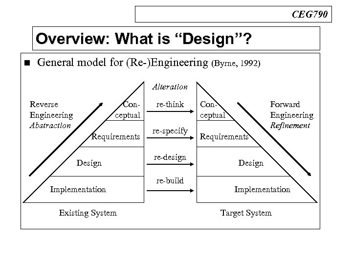 CEG 790 Overview: What is “Design”? n General model for (Re-)Engineering (Byrne, 1992) Alteration Reverse Engineering Abstraction Conceptual Requirements Design Implementation Existing System re-think re-specify re-design re-build Conceptual Forward Engineering Refinement Requirements Design Implementation Target System
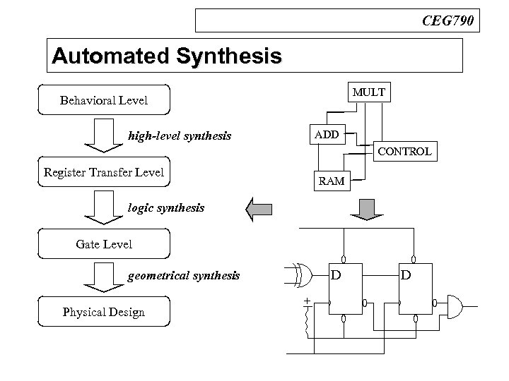
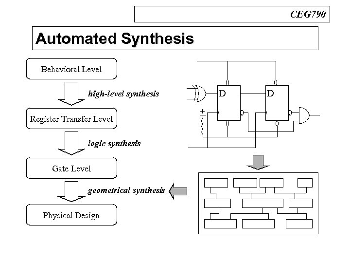
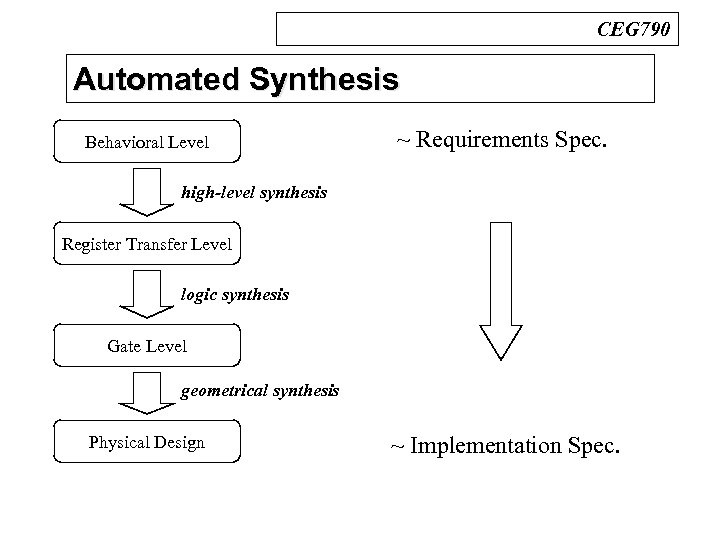 CEG 790 Automated Synthesis n Design Process Behavioral Level ~ Requirements Spec. high-level synthesis Register Transfer Level logic synthesis Gate Level geometrical synthesis Physical Design ~ Implementation Spec.
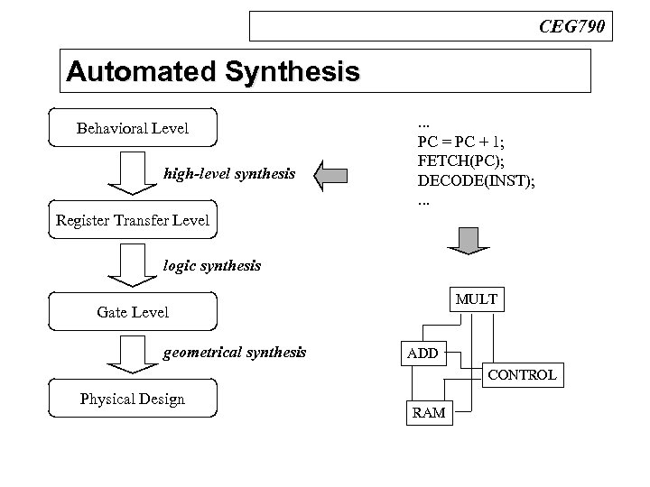 CEG 790 Automated Synthesis n Design Process Behavioral Level high-level synthesis . . . PC = PC + 1; FETCH(PC); DECODE(INST); . . . Register Transfer Level logic synthesis MULT Gate Level geometrical synthesis ADD CONTROL Physical Design RAM
 CEG 790 High-level Synthesis n High-level (Architectural-level) synthesis deals with the transformation of an abstract model of behavior into a model consisting of standard functional units – – Goal: to construct the macroscopic structure of a circuit Input: an abstract model of behavior l – Common Abstract Models: HDLs, State diagrams, ASM charts, Sequencing graphs or Control/Data-flow graphs. Output: a structural view of the circuit, in particular of its datapath, and a logic-level specification of its control unit l often referred to as the register-transfer level or macro-module model
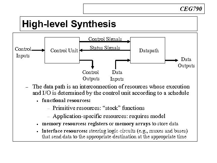 CEG 790 High-level Synthesis Control Signals Control Inputs Control Unit Status Signals Data Outputs Control Outputs – Datapath Data Inputs The data path is an interconnection of resources whose execution and I/O is determined by the control unit according to a schedule l functional resources: – – l l Primitive resources: “stock” functions Application-specific resources: requires model memory resources: registers or memory arrays to store data interface resources: steering logic circuits (e. g. , muxes and buses) that send data to the appropriate destination at the appropriate time
 CEG 790 High-level Synthesis n Measuring cost – – Evaluation Metrics: area, cycle-time (clock period), latency, and throughput (pipelines) The objectives form a n-dimensional design space l l n Architectural exploration is the traversal of the design space to provide a spectrum of solutions for the designers selection Generally only the resources are considered (resource dominant) The fundamental architectural synthesis problem – Explore the design space to minimize “cost” given: l l l A circuit model (behavioral) A set of constraints (on cost) A set of functional resources (characterized for area, delay, etc. )
 CEG 790 Temporal Scheduling n Automated approaches to the fundamental problem consist of two related constrained optimization problems: Temporal Scheduling and Spatial Binding n Temporal Scheduling – Each architectural-level operation is reduced to resource operations and the time interval for the operation execution determined l l l A graph of resources must be created such that one path from start to end exists to perform each operation (in parallel) The length of the path represents the operation latency Constraints include maximum latency, bounds on the resource usage per type, etc.
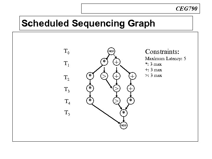 CEG 790 Scheduled Sequencing Graph n BDDs T 0 Constraints: NOP * T 1 + > + + T 2 * T 3 * > + T 4 * > * T 5 * NOP Maximum Latency: 5 *: 3 max +: 3 max >: 3 max
 CEG 790 Spatial Binding n Spatial Binding – Determining the detailed interconnections of the data path and the logic-level specifications of the control unit l l l n The scheduled sequencing graph represents all necessary operations Each resource may cover several operations (for example, an ALU covers addition, subtraction, comparison, etc. ) A simple case is dedicated resource binding - each operation is bound to one resource In general, we wish to share a resources - we don’t need to replicate beyond the maximum number of resources at any given temporal depth In essence, this becomes a set-covering problem (NPC) Once a set of resources is identified, area and performance estimations can be calculated from model data
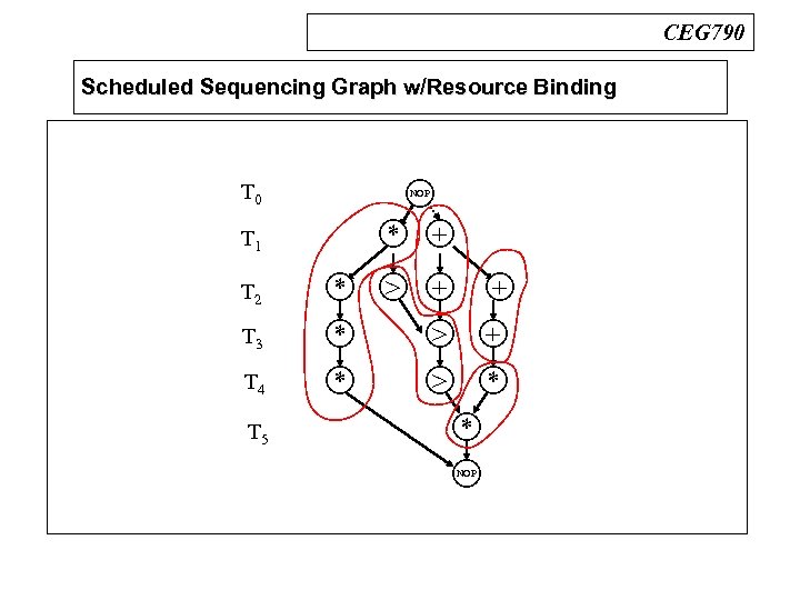 CEG 790 Scheduled Sequencing Graph w/Resource Binding n BDDs T 0 NOP * T 1 + > + + T 2 * T 3 * > + T 4 * > * T 5 * NOP
 CEG 790 Automated Synthesis n Design Process MULT Behavioral Level ADD high-level synthesis CONTROL Register Transfer Level RAM logic synthesis Gate Level D geometrical synthesis Physical Design + D
 CEG 790 Logic-level Synthesis n Logic-level synthesis deals with the transformation of an macroscopic model to an interconnection of logic primitives – n A basic approach is to replace “stock” modules with preoptimized “stock” logic-level representations – – n These primitives determine the microscopic (i. e. , gate-level) structure of the circuit Local optimizations of do not necessarily create an optimal result Cost is increased (area, latency, power) / decreased (design time) Alternatively, the modules are partitioned into manageable designs (generally straightforward for the data path) – Several different types of finite-state machine decompositions exist
 CEG 790 Logic-level Synthesis Tasks n Optimize finite-state machines by state minimization – n Select a state encoding (for control unit) – n Heuristics include one-hot, almost one-hot, minimal-bit change, prioritized-adjacency, etc. Minimize the related combinational component – – n Stated as a bi-partite covering problem Two-level (SOP) minimization (Quine-Mc. Cluksey, Rudell. Sangiovanni, and Mc. Geer algorithms) Multi-level minimization (Decomposition is non-trivial) Cell-library binding – Implement minimized combinational functions as an interconnection of devices that are available in a given technology library (a bound network)
 CEG 790 Automated Synthesis Behavioral Level D high-level synthesis Register Transfer Level logic synthesis Gate Level geometrical synthesis Physical Design + D
 CEG 790 Geometrical-level Synthesis n Geometrical-level synthesis (physical design) consists of creating a physical view at the geometric level – It entails the specification of all geometric patterns defining the physical layout of the chip, as well as their position
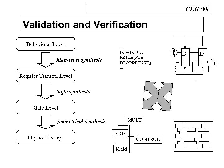 CEG 790 Validation and Verification n Design Process Behavioral Level high-level synthesis . . . PC = PC + 1; FETCH(PC); DECODE(INST); . . . D + Register Transfer Level logic synthesis ? Gate Level MULT geometrical synthesis Physical Design ADD CONTROL RAM D
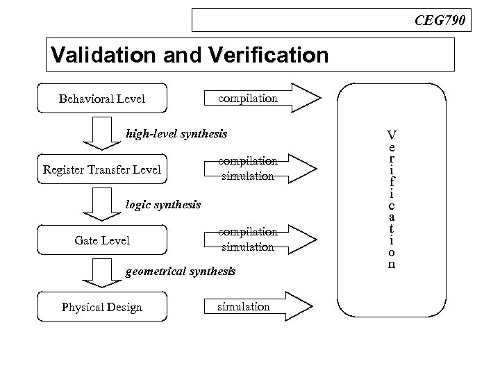 CEG 790 Validation and Verification n Design Process Behavioral Level compilation high-level synthesis Register Transfer Level compilation simulation logic synthesis Gate Level compilation simulation geometrical synthesis Physical Design simulation V e r i f i c a t i o n
 CEG 790 Validation and Verification n Circuit validation consists of acquiring reasonable certainty that a circuit will function correctly – – n Assume no manufacturing fault is present Can be performed via simulation or via verification Simulation (Traditional Validation) – Traditional verification consists of analyzing circuit variables (at different levels) over an interval of time l n Unless exhaustive, simulation does not provide full coverage Formal Verification (Design Verification) – Verification methods mathematically prove or disprove the consistency between two models, or a model and some set of circuit model properties l l Requires a suitable representation system Proofs must be mechanizable
 CEG 790 Formal Verification n Property Testing (Testing via partial specification) – Safety properties: verify “bad things will never occur” l – Liveness properties: verify “good things will occur” l n ex: for every path in the future, at every node on the path, if the Request signal is low, it remain lows until Acknowledge goes low ex: for every path in the future, if there has been a Request signal, then eventually there will be an Acknowledge signal in response to the request on at least one node on the path Popular FV approaches include: – – Theorem Proving Symbolic Model Checking Recursive Learning many graph-based approaches (BDDs, etc. )
 CEG 790 Automated Theorem-Provers n Automated Theorem-Proving techniques require: – – n By means of a rule of inference a new formula can be derived from a given finite set of formulas – – n A representation of the model and/or properties as a series of formulas (axioms) in a High-Order Language A finite collection of rules of inference A formal proof is a finite sequence of formulas, each member of which is either an axiom or the outcome of apply a rule of inference to previous members of the sequence The last formal proof is theorem Allows exhaustive (heuristic directed) search for proof – Theorem-provers presently require extensive user intervention
 CEG 790 Equivalence Checking n Equivalence checking (complete functional testing) – – – The function of an model is equivalent to the function of another if input, state, and output correspondences exist under which the functions are equivalent Many techniques require factorial exploration of the input and state correspondence search space (in the worst-case) FV equivalence checking of designs is known to be intractable l l co-NP complete heuristic techniques to achieve efficient performance
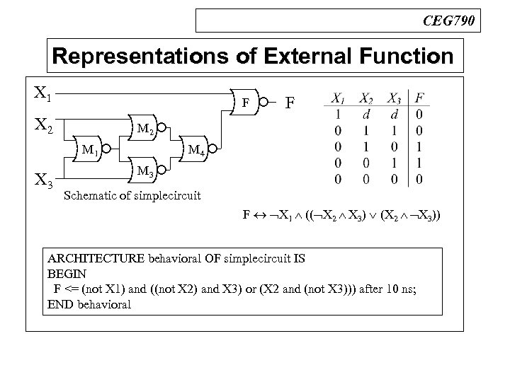 CEG 790 Representations of External Function n BDDs X 1 X 2 F M 2 M 1 X 3 F M 4 M 3 Schematic of simplecircuit F X 1 (( X 2 X 3) (X 2 X 3)) ARCHITECTURE behavioral OF simplecircuit IS BEGIN F <= (not X 1) and ((not X 2) and X 3) or (X 2 and (not X 3))) after 10 ns; END behavioral
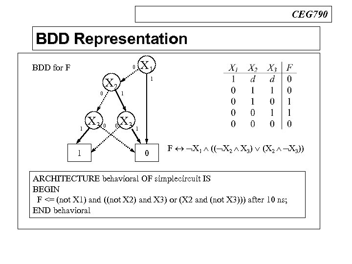 CEG 790 BDD Representation n BDDs BDD for F X 1 0 0 1 1 X 2 X 3 0 0 1 1 X 3 1 0 F X 1 (( X 2 X 3) (X 2 X 3)) ARCHITECTURE behavioral OF simplecircuit IS BEGIN F <= (not X 1) and ((not X 2) and X 3) or (X 2 and (not X 3))) after 10 ns; END behavioral
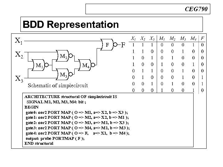 CEG 790 BDD Representation n BDDs X 1 X 2 F M 2 M 1 X 3 F M 4 M 3 Schematic of simplecircuit ARCHITECTURE structural OF simplecircuit IS SIGNAL M 1, M 2, M 3, M 4: bit ; BEGIN gate 0: nor 2 PORT MAP ( O => M 1, a=> X 2, b => X 3 ); gate 1: nor 2 PORT MAP ( O => M 2, a=> X 2, b => M 1 ); gate 2: nor 2 PORT MAP ( O => M 3, a=> M 1, b => X 3 ); gate 3: nor 2 PORT MAP ( O => M 4, a=> M 1, b => M 3 ); gate 4: nor 2 PORT MAP ( O => F, a=> X 1, b => M 4 ); output: probe PORTMAP ( F ); END structural
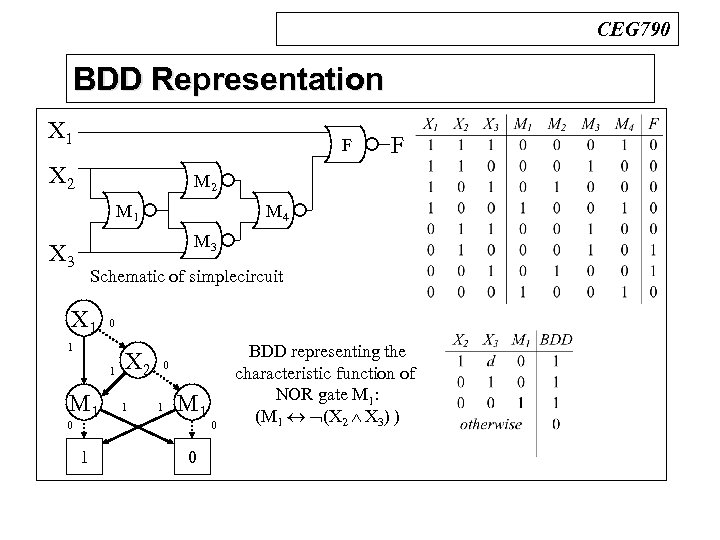 CEG 790 BDD Representation n BDDs X 1 F X 2 F M 2 M 1 M 4 M 3 X 3 Schematic of simplecircuit X 1 0 1 1 M 1 0 1 X 2 1 0 1 M 1 0 0 BDD representing the characteristic function of NOR gate M 1: (M 1 (X 2 X 3) )
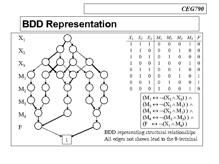 CEG 790 BDD Representation n X 1 BDDs X 2 X 3 M 1 M 2 (M 1 (X 2 X 3) ) (M 2 (X 2 M 1) ) (M 3 (X 3 M 1) ) (M 4 (M 2 M 3) ) (F (X 1 M 4) ) M 3 M 4 F 1 BDD representing structural relationships All edges not shown lead to the 0 -terminal
 CEG 790 Binary Decision Diagrams n n BDDs have been shown to be efficient under a mild assumption on the order of the variables OBDDS have more practical applications than most graphical representations: – – n OBDDs can be transformed into canonical forms to uniquely characterize their function Operations on OBDDs can be done in O(|G|) time OBDDs are the basis for many new FV approaches – – Unfortunately, the size of the BDD is based upon the variable ordering and can have exponential size in the worst case FV problems are far from solved!
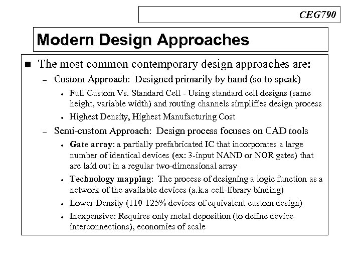 CEG 790 Modern Design Approaches n The most common contemporary design approaches are: – Custom Approach: Designed primarily by hand (so to speak) l l – Full Custom Vs. Standard Cell - Using standard cell designs (same height, variable width) and routing channels simplifies design process Highest Density, Highest Manufacturing Cost Semi-custom Approach: Design process focuses on CAD tools l l Gate array: a partially prefabricated IC that incorporates a large number of identical devices (ex: 3 -input NAND or NOR gates) that are laid out in a regular two-dimensional array Technology mapping: The process of designing a logic function as a network of the available devices (a. k. a cell-library binding) Lower Density (110 -125% devices of equivalent custom design) Inexpensive: Requires only metal deposition (to define device interconnections), economies of scale
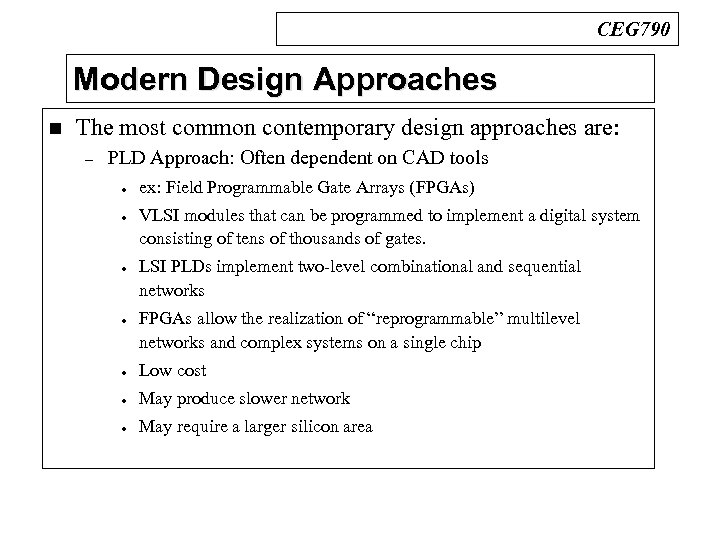 CEG 790 Modern Design Approaches n The most common contemporary design approaches are: – PLD Approach: Often dependent on CAD tools l l ex: Field Programmable Gate Arrays (FPGAs) VLSI modules that can be programmed to implement a digital system consisting of tens of thousands of gates. LSI PLDs implement two-level combinational and sequential networks FPGAs allow the realization of “reprogrammable” multilevel networks and complex systems on a single chip l Low cost l May produce slower network l May require a larger silicon area
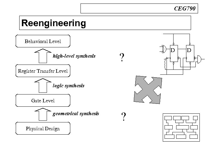 CEG 790 Reengineering n Design Process Behavioral Level high-level synthesis ? Register Transfer Level logic synthesis Gate Level geometrical synthesis Physical Design ? D + D
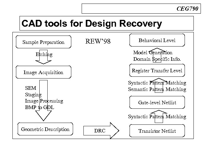 CEG 790 CAD tools for Design Recovery n REW’ 98 Sample Preparation REW’ 98 Behavioral Level Etching Model Generation Domain Specific Info. Image Acquisition Register Transfer Level Syntactic Pattern Matching Semantic Pattern Matching SEM Staging Image Processing BMP to GDL Gate-level Netlist Syntactic Pattern Matching Geometric Description DRC Transistor Netlist


