9f99b3a505ff08af4b054e8b829ec7d7.ppt
- Количество слайдов: 66
 CAE tools and technology challenges in making deep sub-micron IC designs ESE Group seminar 30/3/2010 Kostas Kloukinas CERN, PH-ESE dept. CH 1211, Geneve 23 Switzerland
 Overview n Technology Challenges n Modern CAE Tools n IC design CAE tools at CERN 30/3/10 Kostas. Kloukinas@cern. ch 2
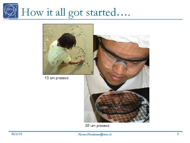 How it all got started…. 10 cm process . 35 um process 30/3/10 Kostas. Kloukinas@cern. ch 3
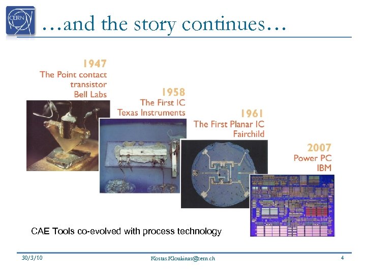 …and the story continues… CAE Tools co-evolved with process technology 30/3/10 Kostas. Kloukinas@cern. ch 4
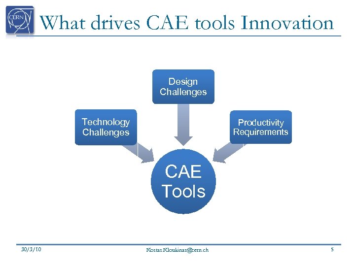 What drives CAE tools Innovation Design Challenges Technology Challenges Productivity Requirements CAE Tools 30/3/10 Kostas. Kloukinas@cern. ch 5
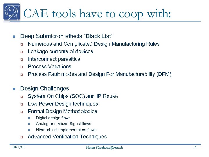 CAE tools have to coop with: n Deep Submicron effects “Black List” q q q n Numerous and Complicated Design Manufacturing Rules Leakage currents of devices Interconnect parasitics Process Variations Process Fault modes and Design For Manufacturability (DFM) Design Challenges q q q System On Chips (SOC) and IP Reuse Low Power Design techniques Formal Design Methodologies n n n q 30/3/10 Digital design flows Analog and Mixed Signal flows Hierarchical Implementation flows Advanced Verification Techniques Kostas. Kloukinas@cern. ch 6
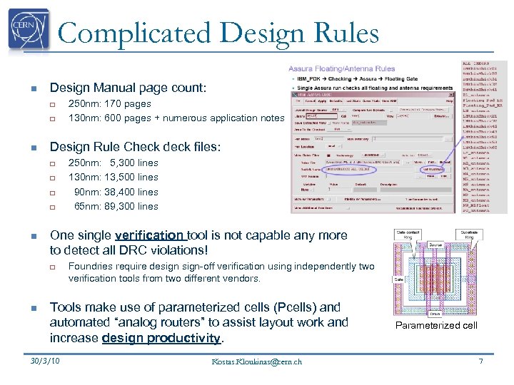 Complicated Design Rules n Design Manual page count: q q n Design Rule Check deck files: q q n 250 nm: 5, 300 lines 130 nm: 13, 500 lines 90 nm: 38, 400 lines 65 nm: 89, 300 lines One single verification tool is not capable any more to detect all DRC violations! q n 250 nm: 170 pages 130 nm: 600 pages + numerous application notes Foundries require design-off verification using independently two verification tools from two different vendors. Tools make use of parameterized cells (Pcells) and automated “analog routers” to assist layout work and increase design productivity. 30/3/10 Kostas. Kloukinas@cern. ch Parameterized cell 7
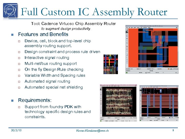 Full Custom IC Assembly Router Tool: Cadence Virtuoso Chip Assembly Router to augment design productivity. n Features and Benefits q q q q n Device, cell, block and top-level chip assembly routing support. Design constraint and process rule driven Interactive signal routing Multi-net/bus routing support On the fly Design Rule checking Variable Width and Spacing rules Automated signal routing Automated special net shielding Requirements: q 30/3/10 Support from foundry PDK with technology specific design rules and constraints. Kostas. Kloukinas@cern. ch 8
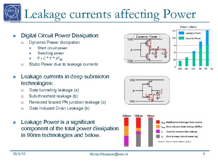 Leakage currents affecting Power n Digital Circuit Power Dissipation q Dynamic Power dissipation n q n Static Power due to leakage currents Leakage currents in deep submicron technologies: q q n Short circuit power Switching power P = C * f * V 2 dd Gate tunneling leakage (a) Sub-threshold leakage (b) Reversed biased PN junction leakage (c) Gate Induced Drain Leakage (b) Leakage Power is a significant component of the total power dissipation in 90 nm technologies and below. 30/3/10 Kostas. Kloukinas@cern. ch 9
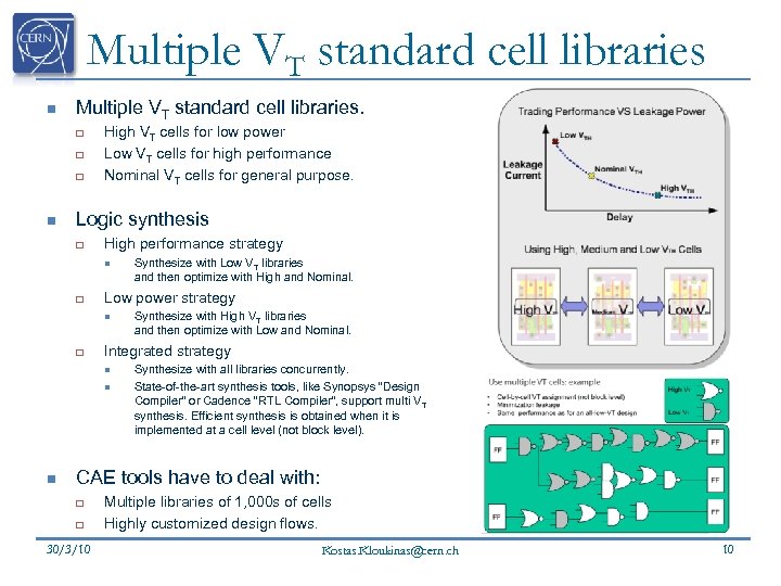 Multiple VT standard cell libraries n Multiple VT standard cell libraries. q q q n High VT cells for low power Low VT cells for high performance Nominal VT cells for general purpose. Logic synthesis q High performance strategy n q Low power strategy n q Synthesize with High VT libraries and then optimize with Low and Nominal. Integrated strategy n n n Synthesize with Low VT libraries and then optimize with High and Nominal. Synthesize with all libraries concurrently. State-of-the-art synthesis tools, like Synopsys “Design Compiler” or Cadence “RTL Compiler”, support multi VT synthesis. Efficient synthesis is obtained when it is implemented at a cell level (not block level). CAE tools have to deal with: q q 30/3/10 Multiple libraries of 1, 000 s of cells Highly customized design flows. Kostas. Kloukinas@cern. ch 10
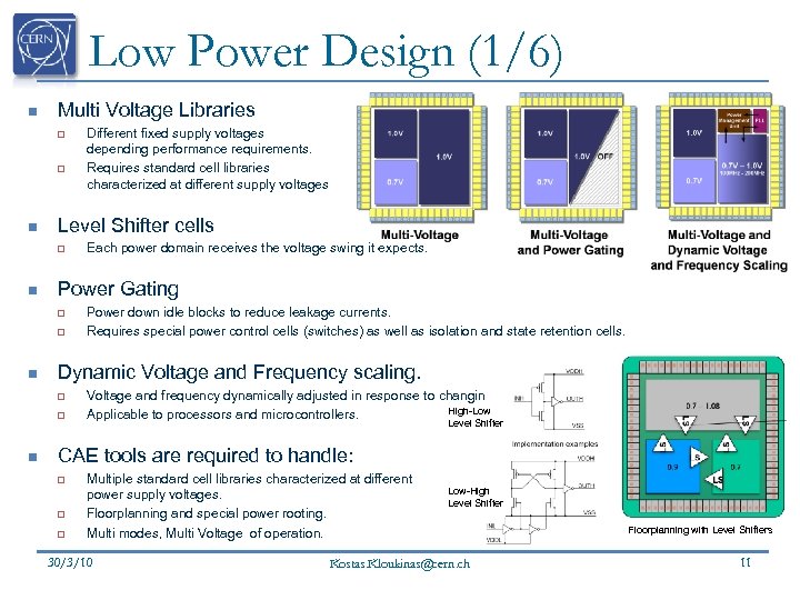 Low Power Design (1/6) n Multi Voltage Libraries q q n Level Shifter cells q n q Power down idle blocks to reduce leakage currents. Requires special power control cells (switches) as well as isolation and state retention cells. Dynamic Voltage and Frequency scaling. q q n Each power domain receives the voltage swing it expects. Power Gating q n Different fixed supply voltages depending performance requirements. Requires standard cell libraries characterized at different supply voltages Voltage and frequency dynamically adjusted in response to changing workloads. High-Low Applicable to processors and microcontrollers. Level Shifter CAE tools are required to handle: q q q Multiple standard cell libraries characterized at different power supply voltages. Floorplanning and special power rooting. Multi modes, Multi Voltage of operation. 30/3/10 Low-High Level Shifter Kostas. Kloukinas@cern. ch Floorplanning with Level Shifters 11
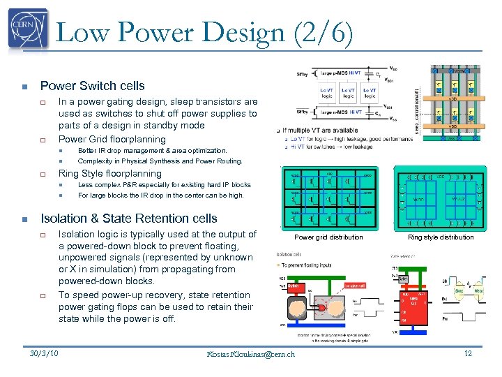 Low Power Design (2/6) n Power Switch cells q q In a power gating design, sleep transistors are used as switches to shut off power supplies to parts of a design in standby mode Power Grid floorplanning n n q Ring Style floorplanning n n n Better IR drop management & area optimization. Complexity in Physical Synthesis and Power Routing. Less complex P&R especially for existing hard IP blocks For large blocks the IR drop in the center can be high. Isolation & State Retention cells q q 30/3/10 Isolation logic is typically used at the output of a powered-down block to prevent floating, unpowered signals (represented by unknown or X in simulation) from propagating from powered-down blocks. To speed power-up recovery, state retention power gating flops can be used to retain their state while the power is off. Power grid distribution Ring style distribution Kostas. Kloukinas@cern. ch 12
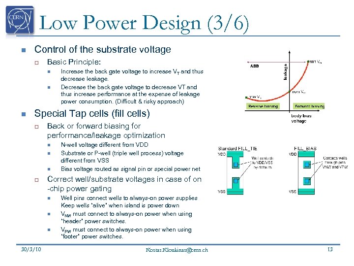 Low Power Design (3/6) n Control of the substrate voltage q Basic Principle: n n n Increase the back gate voltage to increase VT and thus decrease leakage. Decrease the back gate voltage to decrease VT and thus increase performance at the expense of leakage power consumption. (Difficult & risky approach) Special Tap cells (fill cells) q Back or forward biasing for performance/leakage optimization n q Correct well/substrate voltages in case of on -chip power gating n n n 30/3/10 N-well voltage different from VDD Substrate or P-well (triple well process) voltage different from VSS Bias voltage routed as signal pin or special power net Well pins connect wells to always-on power supplies Keep wells “alive” when island is power down VNW must connect to always-on power when using “header” power switches. VPW must connect to always-on power when using “footer” power switches. Kostas. Kloukinas@cern. ch 13
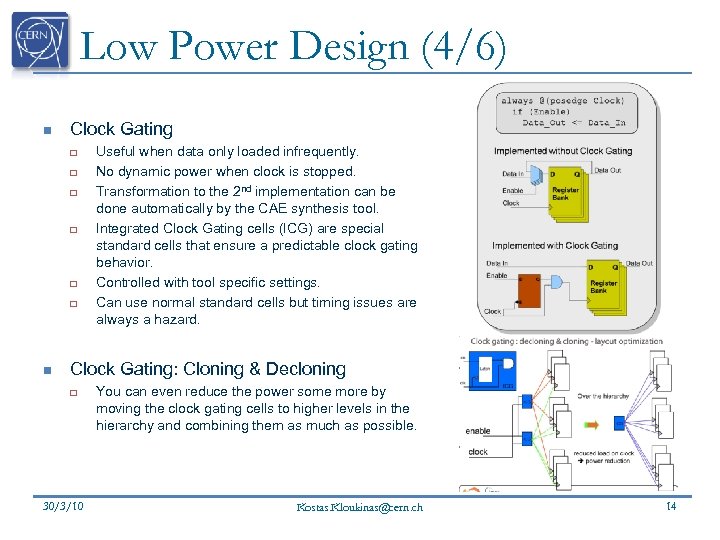 Low Power Design (4/6) n Clock Gating q q q n Useful when data only loaded infrequently. No dynamic power when clock is stopped. Transformation to the 2 nd implementation can be done automatically by the CAE synthesis tool. Integrated Clock Gating cells (ICG) are special standard cells that ensure a predictable clock gating behavior. Controlled with tool specific settings. Can use normal standard cells but timing issues are always a hazard. Clock Gating: Cloning & Decloning q 30/3/10 You can even reduce the power some more by moving the clock gating cells to higher levels in the hierarchy and combining them as much as possible. Kostas. Kloukinas@cern. ch 14
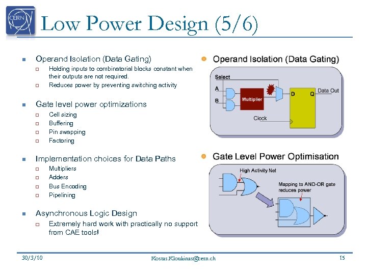 Low Power Design (5/6) n Operand Isolation (Data Gating) q q n Gate level power optimizations q q n Cell sizing Buffering Pin swapping Factoring Implementation choices for Data Paths q q n Holding inputs to combinatorial blocks constant when their outputs are not required. Reduces power by preventing switching activity Multipliers Adders Bus Encoding Pipelining Asynchronous Logic Design q 30/3/10 Extremely hard work with practically no support from CAE tools! Kostas. Kloukinas@cern. ch 15
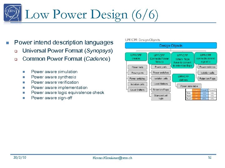 Low Power Design (6/6) n Power intend description languages q q Universal Power Format (Synopsys) Common Power Format (Cadence) n n n 30/3/10 Power aware simulation Power aware synthesis Power aware verification Power aware implementation Power aware logic equivalence check Power aware sign-off Kostas. Kloukinas@cern. ch 16
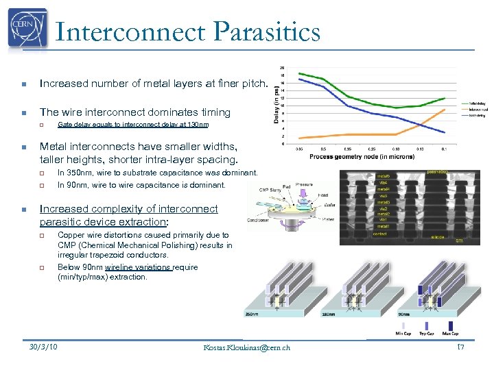 Interconnect Parasitics n Increased number of metal layers at finer pitch. n The wire interconnect dominates timing q n Metal interconnects have smaller widths, taller heights, shorter intra-layer spacing. q q n Gate delay equals to interconnect delay at 130 nm. In 350 nm, wire to substrate capacitance was dominant. In 90 nm, wire to wire capacitance is dominant. Increased complexity of interconnect parasitic device extraction: q q 30/3/10 Copper wire distortions caused primarily due to CMP (Chemical Mechanical Polishing) results in irregular trapezoid conductors. Below 90 nm wireline variations require (min/typ/max) extraction. Kostas. Kloukinas@cern. ch 17
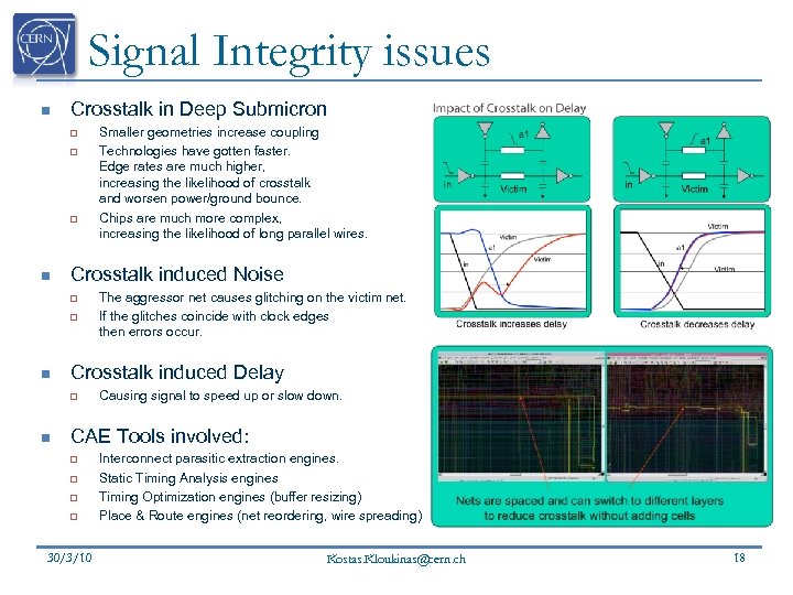 Signal Integrity issues n Crosstalk in Deep Submicron q q q n Crosstalk induced Noise q q n The aggressor net causes glitching on the victim net. If the glitches coincide with clock edges then errors occur. Crosstalk induced Delay q n Smaller geometries increase coupling Technologies have gotten faster. Edge rates are much higher, increasing the likelihood of crosstalk and worsen power/ground bounce. Chips are much more complex, increasing the likelihood of long parallel wires. Causing signal to speed up or slow down. CAE Tools involved: q q 30/3/10 Interconnect parasitic extraction engines. Static Timing Analysis engines Timing Optimization engines (buffer resizing) Place & Route engines (net reordering, wire spreading) Kostas. Kloukinas@cern. ch 18
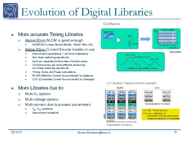 Evolution of Digital Libraries n More accurate Timing Libraries q Above 90 nm NLDM is good enough n q Below 90 nm Current Source models in use n n n n NLDM (Non Linear Device Model) “liberty” files (. lib) Interconnect capacitance > cell drive impedance. Non linear switching waveforms. Input pin capacitance becomes a function slope. Current sources are more effective at tracking non-linear switching waveforms. Timing, Noise and Power calculations. ECSM (Effective Current Source Model) by Cadence CCS (Composite Current Source model) by Synopsys More Libraries due to: q q q Multi-VT options Multi-voltage options Multi-corners due to process parameters: n n 30/3/10 Tox, VTh variations Interconnect variations Kostas. Kloukinas@cern. ch 19
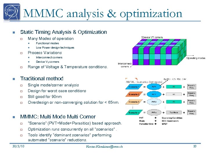 MMMC analysis & optimization n Static Timing Analysis & Optimization q Many Modes of operation n n q Process Variations n n q n Interconnect corners Device VT corners Range of Voltage & Temperature conditions. Traditional method q q n Functional modes Low Power design techniques Single mode/corner analysis Design for worst case conditions Still good for 90 nm Overdesign or non-converging solution for < 65 nm. MMMC: Multi Mode Multi Corner q q q 30/3/10 “Scenario” (PVT+Mode+Parasitics) based approach. Optimization runs concurrently on all “scenarios”. Tools identify “dominant scenarios” performing automated “scenario” reductions. Kostas. Kloukinas@cern. ch 20
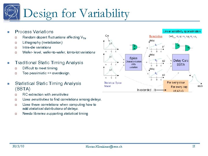 Design for Variability n Process Variations q q n Traditional Static Timing Analysis q q n Random dopant fluctuations affecting VTH Lithography (metalization) Intra-die variations Wafer- level, wafer-to-wafer, lot-to-lot variations Difficult to meet timimg Too pessimistic => overdesign. Statistical Static Timing Analysis (SSTA) q q RC extraction with sensitivites Uses sensitivities to find correlations among delays. Uses these correlations when computing how to add statistical distributions of delays. Needs libraries supporting statistical timing 30/3/10 Kostas. Kloukinas@cern. ch 21
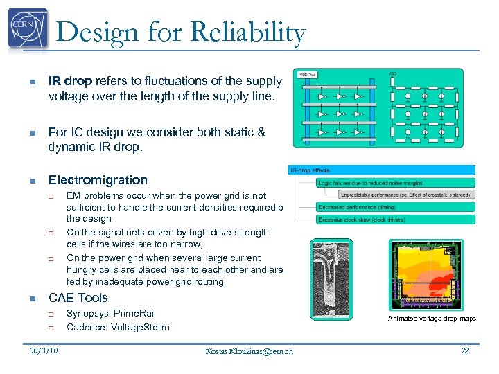 Design for Reliability n IR drop refers to fluctuations of the supply voltage over the length of the supply line. n For IC design we consider both static & dynamic IR drop. n Electromigration q q q n EM problems occur when the power grid is not sufficient to handle the current densities required by the design. On the signal nets driven by high drive strength cells if the wires are too narrow, On the power grid when several large current hungry cells are placed near to each other and are fed by inadequate power grid routing. CAE Tools q q 30/3/10 Synopsys: Prime. Rail Cadence: Voltage. Storm Animated voltage drop maps Kostas. Kloukinas@cern. ch 22
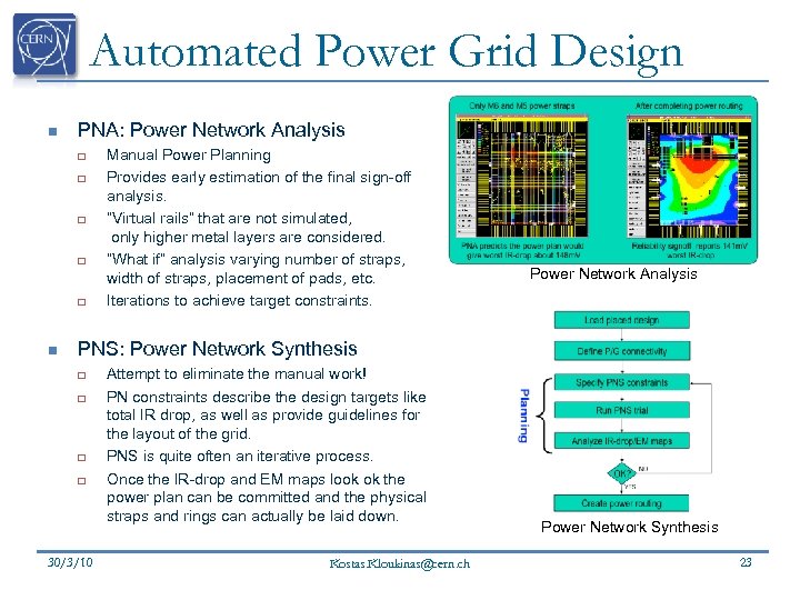 Automated Power Grid Design n PNA: Power Network Analysis q q q n Manual Power Planning Provides early estimation of the final sign-off analysis. “Virtual rails” that are not simulated, only higher metal layers are considered. “What if” analysis varying number of straps, width of straps, placement of pads, etc. Iterations to achieve target constraints. Power Network Analysis PNS: Power Network Synthesis q q 30/3/10 Attempt to eliminate the manual work! PN constraints describe the design targets like total IR drop, as well as provide guidelines for the layout of the grid. PNS is quite often an iterative process. Once the IR-drop and EM maps look ok the power plan can be committed and the physical straps and rings can actually be laid down. Kostas. Kloukinas@cern. ch Power Network Synthesis 23
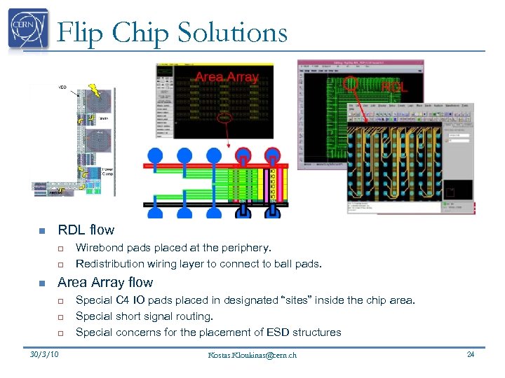 Flip Chip Solutions n RDL flow q q n Wirebond pads placed at the periphery. Redistribution wiring layer to connect to ball pads. Area Array flow q q q 30/3/10 Special C 4 IO pads placed in designated “sites” inside the chip area. Special short signal routing. Special concerns for the placement of ESD structures Kostas. Kloukinas@cern. ch 24
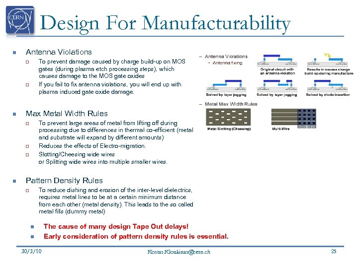 Design For Manufacturability n Antenna Violations To prevent damage caused by charge build-up on MOS gates (during plasma etch processing steps), which causes damage to the MOS gate oxides If you fail to fix antenna violations, you will end up with plasma induced gate oxide damage. q q n Max Metal Width Rules To prevent large areas of metal from lifting off during processing due to differences in thermal co-efficient (metal and substrate will expand by different amounts) Reduces the effects of Electro-migration. Slotting/Cheesing wide wires or Splitting wide wires into multiple smaller wires. q q q n Pattern Density Rules To reduce dishing and erosion of the inter-level dielectrics, requires metal lines to be at a certain minimum distance from each other (metal density). This leads to the so called metal fills (dummy metal) q n n 30/3/10 The cause of many design Tape Out delays! Early consideration of pattern density rules is essential. Kostas. Kloukinas@cern. ch 25
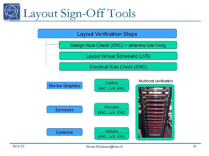 Layout Sign-Off Tools 30/3/10 Kostas. Kloukinas@cern. ch 26
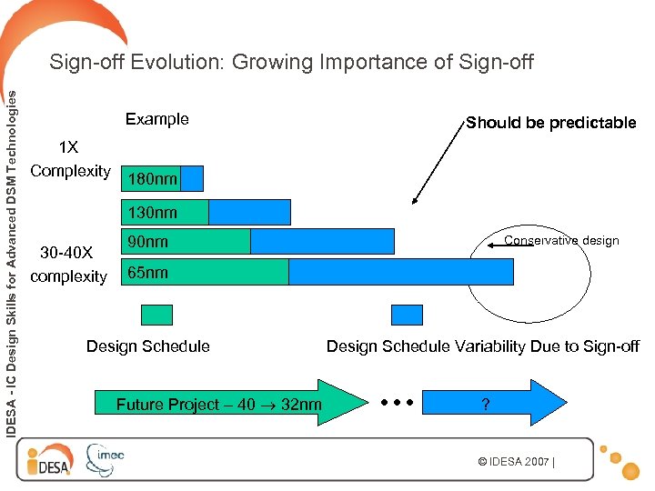 IDESA - IC Design Skills for Advanced DSM Technologies Sign-off Evolution: Growing Importance of Sign-off Example 1 X Complexity Should be predictable 180 nm 130 nm 30 -40 X complexity 90 nm Conservative design 65 nm Design Schedule Future Project – 40 32 nm Design Schedule Variability Due to Sign-off ? © IDESA 2007 |
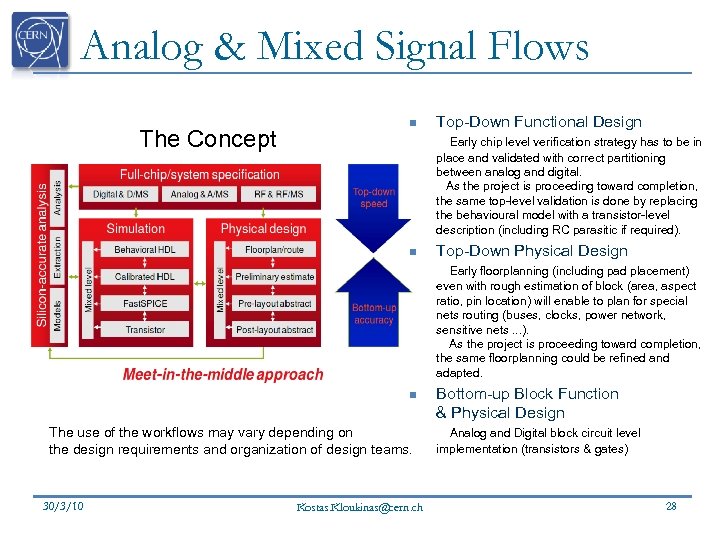 Analog & Mixed Signal Flows The Concept n Top-Down Functional Design Early chip level verification strategy has to be in place and validated with correct partitioning between analog and digital. As the project is proceeding toward completion, the same top-level validation is done by replacing the behavioural model with a transistor-level description (including RC parasitic if required). n Top-Down Physical Design Early floorplanning (including pad placement) even with rough estimation of block (area, aspect ratio, pin location) will enable to plan for special nets routing (buses, clocks, power network, sensitive nets. . . ). As the project is proceeding toward completion, the same floorplanning could be refined and adapted. n The use of the workflows may vary depending on the design requirements and organization of design teams. 30/3/10 Kostas. Kloukinas@cern. ch Bottom-up Block Function & Physical Design Analog and Digital block circuit level implementation (transistors & gates) 28
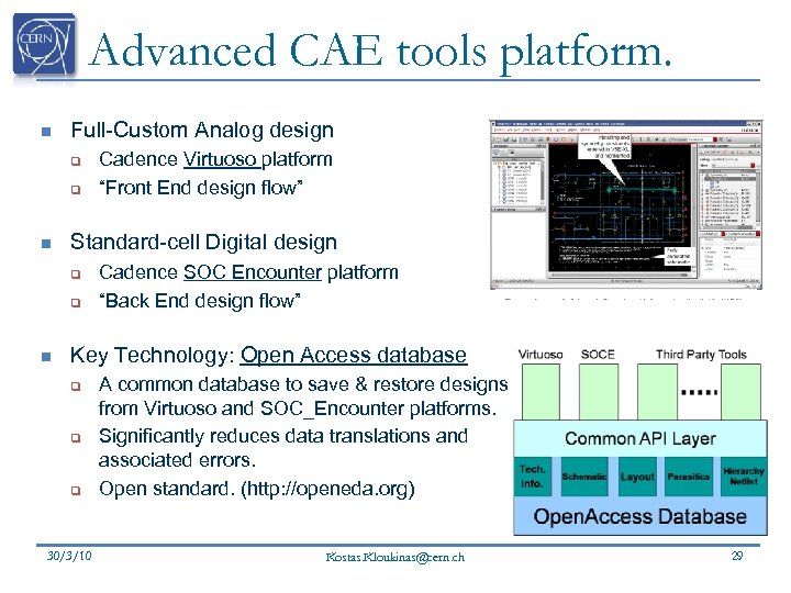 Advanced CAE tools platform. n Full-Custom Analog design q q n Standard-cell Digital design q q n Cadence Virtuoso platform “Front End design flow” Cadence SOC Encounter platform “Back End design flow” Key Technology: Open Access database q q q 30/3/10 A common database to save & restore designs from Virtuoso and SOC_Encounter platforms. Significantly reduces data translations and associated errors. Open standard. (http: //openeda. org) Kostas. Kloukinas@cern. ch 29
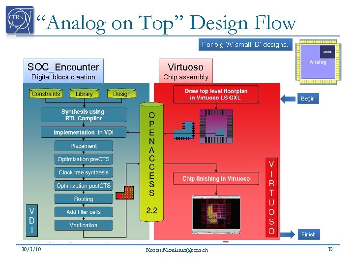 “Analog on Top” Design Flow For big ‘A’ small ‘D’ designs. SOC_Encounter Virtuoso Digital block creation Chip assembly Begin Finish 30/3/10 Kostas. Kloukinas@cern. ch 30
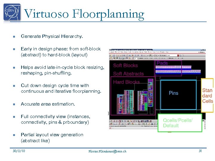 Virtuoso Floorplanning n Generate Physical Hierarchy. n Early in design phase: from soft-block (abstract) to hard-block (layout) n Helps avoid late-in-cycle block resizing, reshaping, pin-shuffling. n Cut down design cycle time with continuous and iterative floorplanning. n Accurate area estimation. n Full connectivity view (instances, connectivity, pins & prboundary) n Partial layout view generation (abstract like) 30/3/10 Kostas. Kloukinas@cern. ch 31
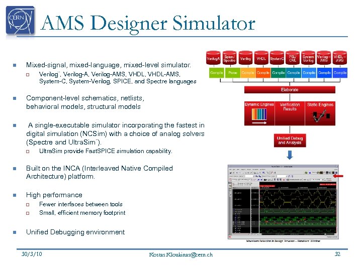 AMS Designer Simulator n Mixed-signal, mixed-language, mixed-level simulator. q Verilog¨, Verilog-AMS, VHDL-AMS, System-C, System-Verilog, SPICE, and Spectre languages n Component-level schematics, netlists, behavioral models, structural models n A single-executable simulator incorporating the fastest in digital simulation (NCSim) with a choice of analog solvers (Spectre and Ultra. Sim¨). q Ultra. Sim provide Fast. SPICE simulation capability. n Built on the INCA (Interleaved Native Compiled Architecture) platform. n High performance q q n Fewer interfaces between tools Small, efficient memory footprint Unified Debugging environment 30/3/10 Kostas. Kloukinas@cern. ch 32
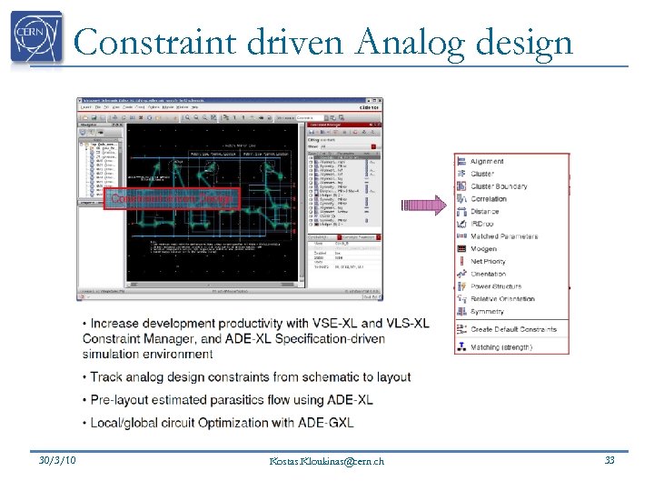 Constraint driven Analog design 30/3/10 Kostas. Kloukinas@cern. ch 33
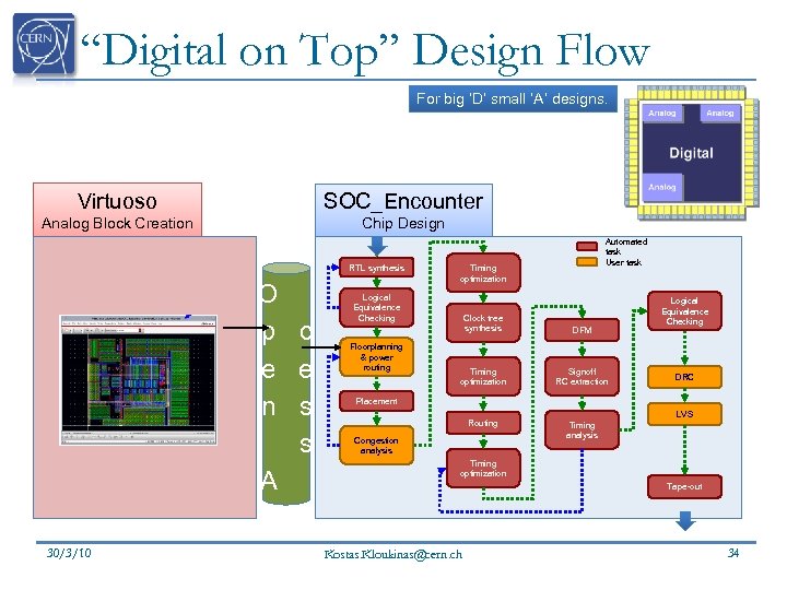 “Digital on Top” Design Flow For big ‘D’ small ‘A’ designs. Virtuoso SOC_Encounter Analog Block Creation Chip Design RTL synthesis O p e n A c 30/3/10 c e s s Automated task User task Timing optimization Logical Equivalence Checking DFM Timing optimization Signoff RC extraction Routing Floorplanning & power routing Clock tree synthesis Logical Equivalence Checking Timing analysis DRC Placement Congestion analysis LVS Timing optimization Tape-out Kostas. Kloukinas@cern. ch 34
 IC design CAE tools at CERN 30/3/10 Kostas. Kloukinas@cern. ch 35
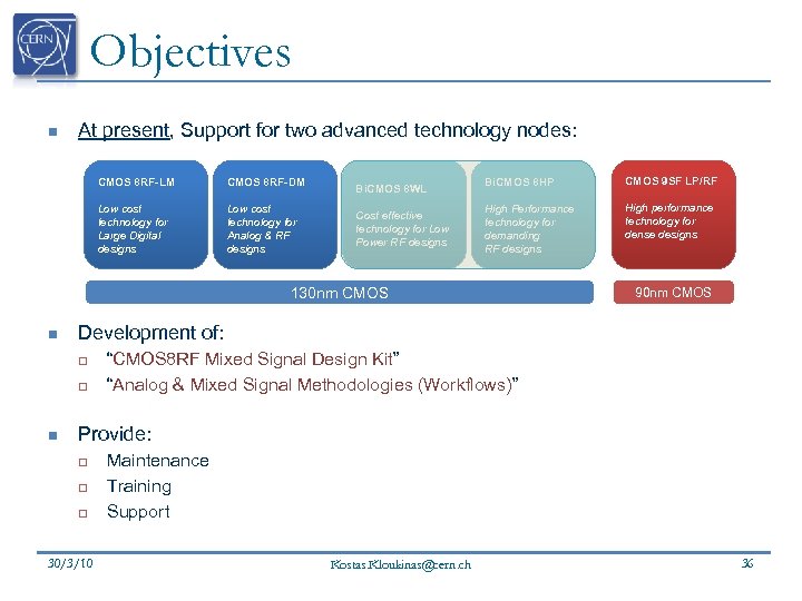 Objectives n At present, Support for two advanced technology nodes: CMOS 8 RF-LM CMOS 8 RF-DM Low cost technology for Large Digital designs Low cost technology for Analog & RF designs Bi. CMOS 8 WL Cost effective technology for Low Power RF designs Bi. CMOS 8 HP CMOS 9 SF LP/RF High Performance technology for demanding RF designs High performance technology for dense designs 130 nm CMOS n Development of: q q n 90 nm CMOS “CMOS 8 RF Mixed Signal Design Kit” “Analog & Mixed Signal Methodologies (Workflows)” Provide: q q q 30/3/10 Maintenance Training Support Kostas. Kloukinas@cern. ch 36
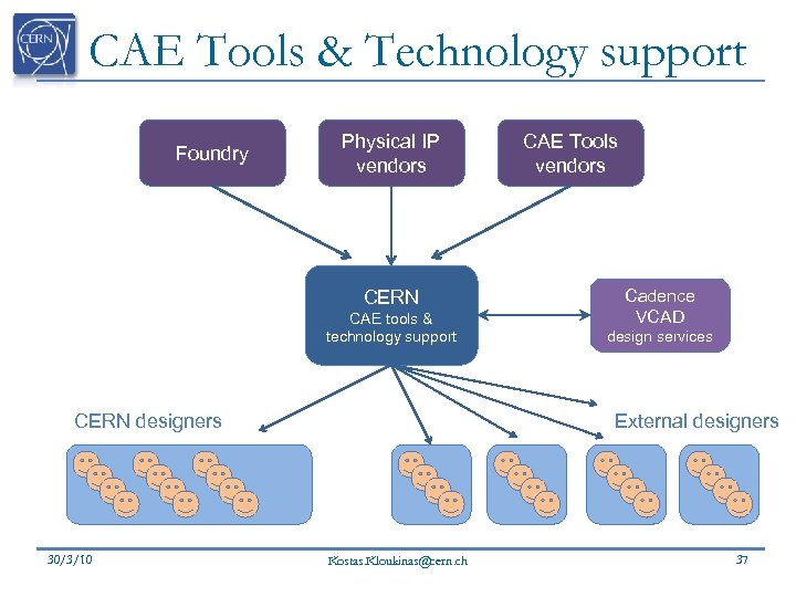 CAE Tools & Technology support Foundry Physical IP vendors CERN CAE tools & technology support CERN designers 30/3/10 CAE Tools vendors Cadence VCAD design services External designers Kostas. Kloukinas@cern. ch 37
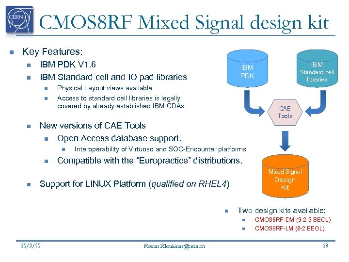 CMOS 8 RF Mixed Signal design kit n Key Features: n n IBM PDK V 1. 6 IBM Standard cell and IO pad libraries n n n IBM PDK Physical Layout views available. Access to standard cell libraries is legally covered by already established IBM CDAs Standard cell libraries CAE Tools New versions of CAE Tools n Open Access database support. n n Interoperability of Virtuoso and SOC-Encounter platforms. Compatible with the “Europractice” distributions. Mixed Signal n Design Kit Support for LINUX Platform (qualified on RHEL 4) n Two design kits available: n n 30/3/10 Kostas. Kloukinas@cern. ch CMOS 8 RF-DM (3 -2 -3 BEOL) CMOS 8 RF-LM (6 -2 BEOL) 38
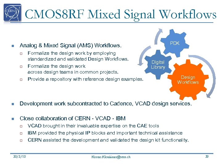 CMOS 8 RF Mixed Signal Workflows n PDK Analog & Mixed Signal (AMS) Workflows. q q q Formalize the design work by employing standardized and validated Design Workflows. Formalize the design work across design teams in common projects. Provide a repository with reference design examples. Digital Library Design Workflows n Development work subcontracted to Cadence, VCAD design services. n Close collaboration of CERN - VCAD - IBM q q q 30/3/10 VCAD brought in their invaluable expertise on the CAE tools IBM provided the physical IP blocks and important technical assistance CERN assisted the development and validated the design kit functionality. Kostas. Kloukinas@cern. ch 39
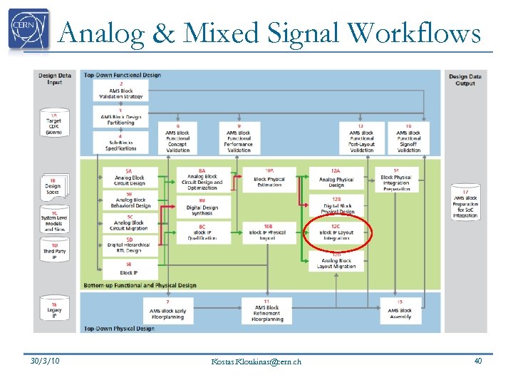 Analog & Mixed Signal Workflows 30/3/10 Kostas. Kloukinas@cern. ch 40
 Digital Block Implementation Flow “I 2 C slave” serial interface IP block employing Triple Module Redundancy for enhanced SEU protection. Prepared by Sandro Bonacini CERN PH/ESE sandro. bonacini@cern. ch 30/3/10 Kostas. Kloukinas@cern. ch 41
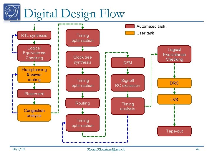 Digital Design Flow Automated task RTL synthesis Logical Equivalence Checking Floorplanning & power routing User task Timing optimization Clock tree synthesis DFM Timing optimization Signoff RC extraction Logical Equivalence Checking DRC Placement Routing Congestion analysis Timing analysis LVS Timing optimization Tape-out 30/3/10 Kostas. Kloukinas@cern. ch 42
![Synthesis sandro. bonacini@cern. ch Timing constraints [. sdc] Max timing Liberty libraries [. lib] Synthesis sandro. bonacini@cern. ch Timing constraints [. sdc] Max timing Liberty libraries [. lib]](https://present5.com/presentation/9f99b3a505ff08af4b054e8b829ec7d7/image-43.jpg) Synthesis sandro. bonacini@cern. ch Timing constraints [. sdc] Max timing Liberty libraries [. lib] RTL description [. v] / [. vhd] RTL synthesis Synthesis, mapping and timing reports Capacitance tables [. Cap. Tbl] Abstract layout Definition [. lef] Mapped netlist [. v] Conformal script [. lec] RTL compiler script [. tcl] 30/3/10 Kostas. Kloukinas@cern. ch 43
Synthesis sandro. bonacini@cern. ch Timing constraints [. sdc] Max timing Liberty libraries [. lib] RTL description [. v] / [. vhd] RTL synthesis Synthesis, mapping and timing reports Capacitance tables [. Cap. Tbl] Abstract layout Definition [. lef] Mapped netlist [. v] Conformal script [. lec] RTL compiler script [. tcl] 30/3/10 Kostas. Kloukinas@cern. ch 43
![Logic Equivalent Checking (LEC) sandro. bonacini@cern. ch RTL description [. v] / [. vhd] Logic Equivalent Checking (LEC) sandro. bonacini@cern. ch RTL description [. v] / [. vhd]](https://present5.com/presentation/9f99b3a505ff08af4b054e8b829ec7d7/image-44.jpg) Logic Equivalent Checking (LEC) sandro. bonacini@cern. ch RTL description [. v] / [. vhd] Mapped netlist [. v] Conformal script [. lec] Max timing Liberty libraries [. lib] Logical Equivalence Checking n LEC report 30/3/10 Kostas. Kloukinas@cern. ch Tool: Conformal 44
Logic Equivalent Checking (LEC) sandro. bonacini@cern. ch RTL description [. v] / [. vhd] Mapped netlist [. v] Conformal script [. lec] Max timing Liberty libraries [. lib] Logical Equivalence Checking n LEC report 30/3/10 Kostas. Kloukinas@cern. ch Tool: Conformal 44
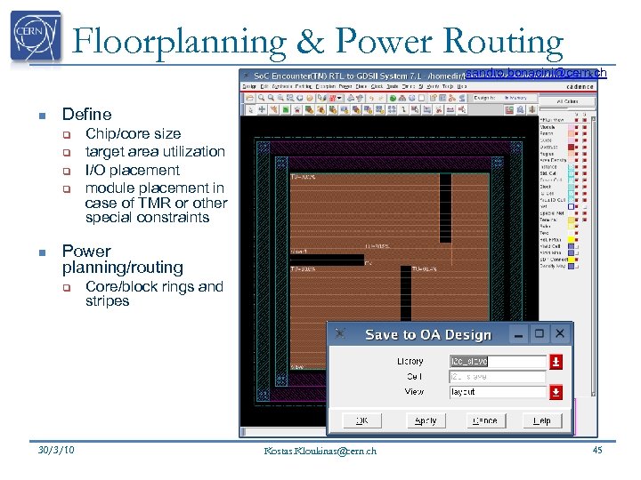 Floorplanning & Power Routing sandro. bonacini@cern. ch n Define q q n Chip/core size target area utilization I/O placement module placement in case of TMR or other special constraints Power planning/routing q 30/3/10 Core/block rings and stripes Kostas. Kloukinas@cern. ch 45
![Placement sandro. bonacini@cern. ch n Encounter command file Open Access Floorplanned Design [. oa] Placement sandro. bonacini@cern. ch n Encounter command file Open Access Floorplanned Design [. oa]](https://present5.com/presentation/9f99b3a505ff08af4b054e8b829ec7d7/image-46.jpg) Placement sandro. bonacini@cern. ch n Encounter command file Open Access Floorplanned Design [. oa] Connect cells power/ground Add tap cells Placement Scan-chain reorder Reports 30/3/10 Open Access Placed Design [. oa] Kostas. Kloukinas@cern. ch 46
Placement sandro. bonacini@cern. ch n Encounter command file Open Access Floorplanned Design [. oa] Connect cells power/ground Add tap cells Placement Scan-chain reorder Reports 30/3/10 Open Access Placed Design [. oa] Kostas. Kloukinas@cern. ch 46
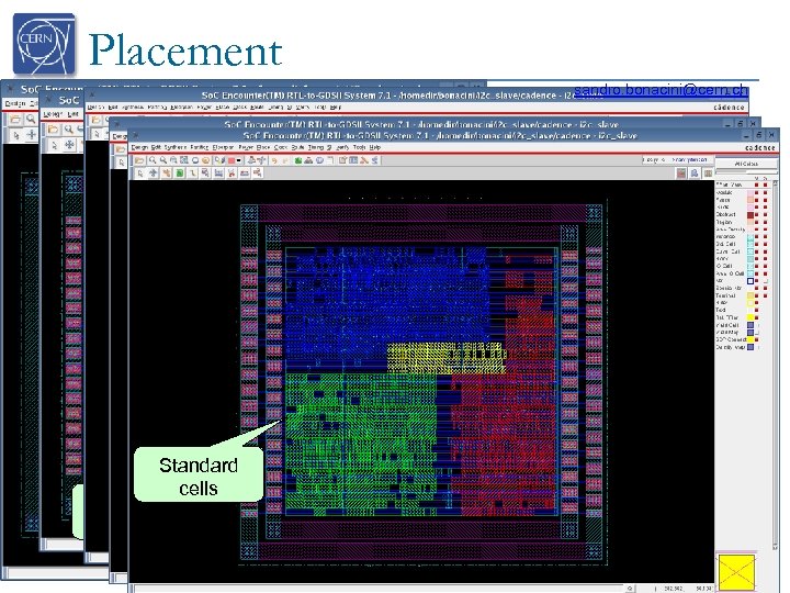 Placement sandro. bonacini@cern. ch Tap cells Standard cells Power/ground connections 30/3/10 Sandro Bonacini - PH/ESE - sandro. bonacini@cern. ch Kostas. Kloukinas@cern. ch 47
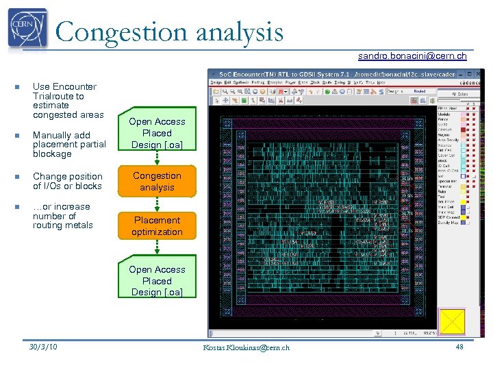 Congestion analysis sandro. bonacini@cern. ch n Use Encounter Trialroute to estimate congested areas n Manually add placement partial blockage n Change position of I/Os or blocks n …or increase number of routing metals Open Access Placed Design [. oa] Congestion analysis Placement optimization Open Access Placed Design [. oa] 30/3/10 Kostas. Kloukinas@cern. ch 48
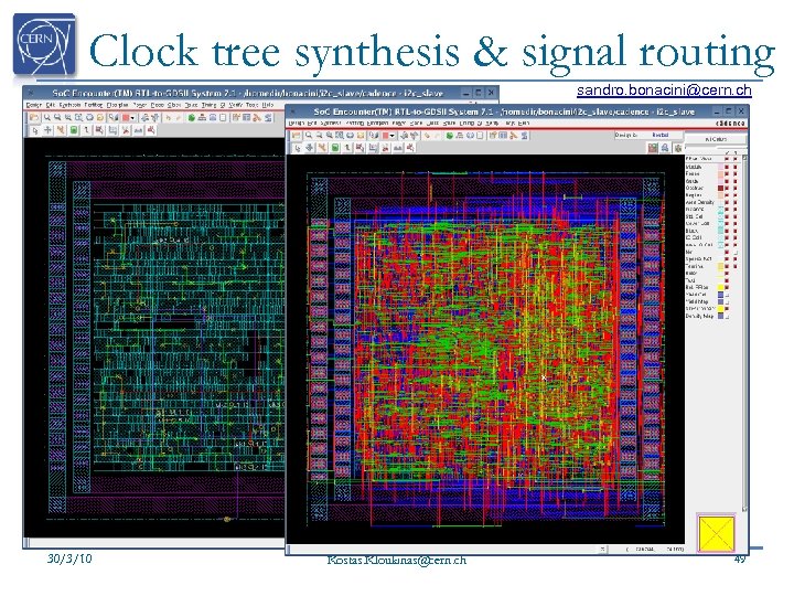 Clock tree synthesis & signal routing sandro. bonacini@cern. ch 30/3/10 Kostas. Kloukinas@cern. ch 49
![Design For Manufacturing sandro. bonacini@cern. ch Open Access Routed Design [. oa] Antenna fix Design For Manufacturing sandro. bonacini@cern. ch Open Access Routed Design [. oa] Antenna fix](https://present5.com/presentation/9f99b3a505ff08af4b054e8b829ec7d7/image-50.jpg) Design For Manufacturing sandro. bonacini@cern. ch Open Access Routed Design [. oa] Antenna fix Via optimization Cells & metal fill Signoff RC extraction Final netlist [. v] Open Access Final Design [. oa] Signal integrity analysis Delay file [. sdf] Timing analysis Signoff timing report 30/3/10 Kostas. Kloukinas@cern. ch 50
Design For Manufacturing sandro. bonacini@cern. ch Open Access Routed Design [. oa] Antenna fix Via optimization Cells & metal fill Signoff RC extraction Final netlist [. v] Open Access Final Design [. oa] Signal integrity analysis Delay file [. sdf] Timing analysis Signoff timing report 30/3/10 Kostas. Kloukinas@cern. ch 50
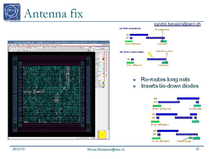 Antenna fix sandro. bonacini@cern. ch n n 30/3/10 Kostas. Kloukinas@cern. ch Re-routes long nets Inserts tie-down diodes 51
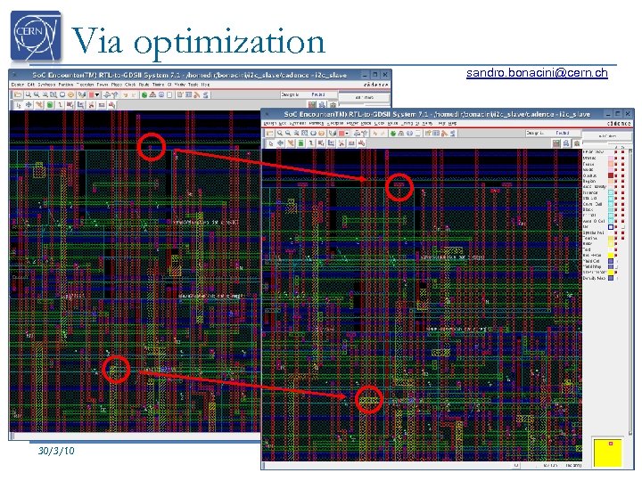 Via optimization sandro. bonacini@cern. ch 30/3/10 Kostas. Kloukinas@cern. ch 52
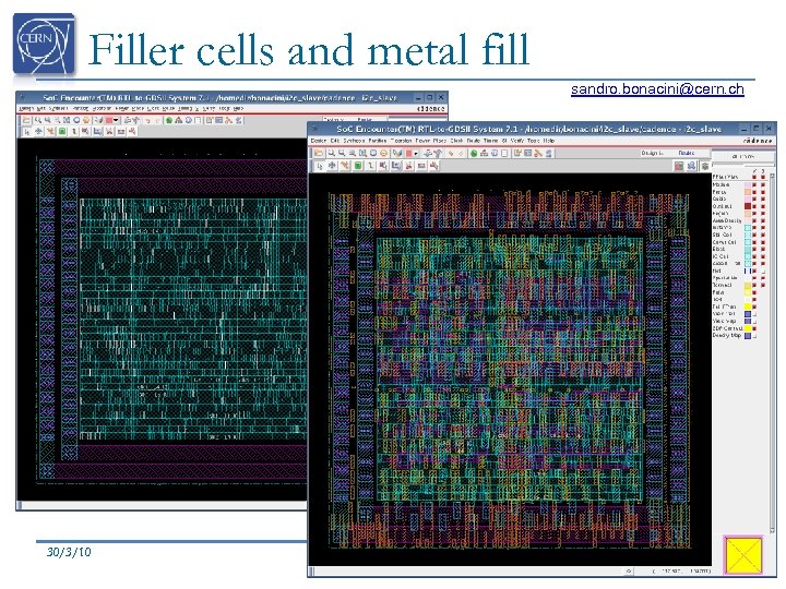 Filler cells and metal fill sandro. bonacini@cern. ch 30/3/10 Kostas. Kloukinas@cern. ch 53
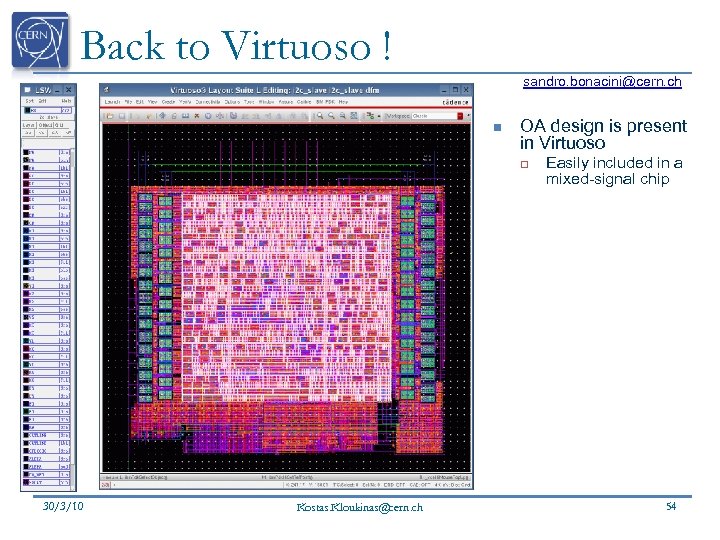 Back to Virtuoso ! sandro. bonacini@cern. ch n OA design is present in Virtuoso q 30/3/10 Kostas. Kloukinas@cern. ch Easily included in a mixed-signal chip 54
 Training: AMS Workshops n Workshop Targets: q q q n Present the IBM CMOS 8 RF (130 nm) Mixed Signal Kit. Present Workflows for Analog, Digital and Mixed Signal designs. Introduce the new Platform of Cadence CAE Tools. This is NOT: q q 30/3/10 A course on analog or digital designing. An advanced course targeted to a specific Cadence Tool. Kostas. Kloukinas@cern. ch 55
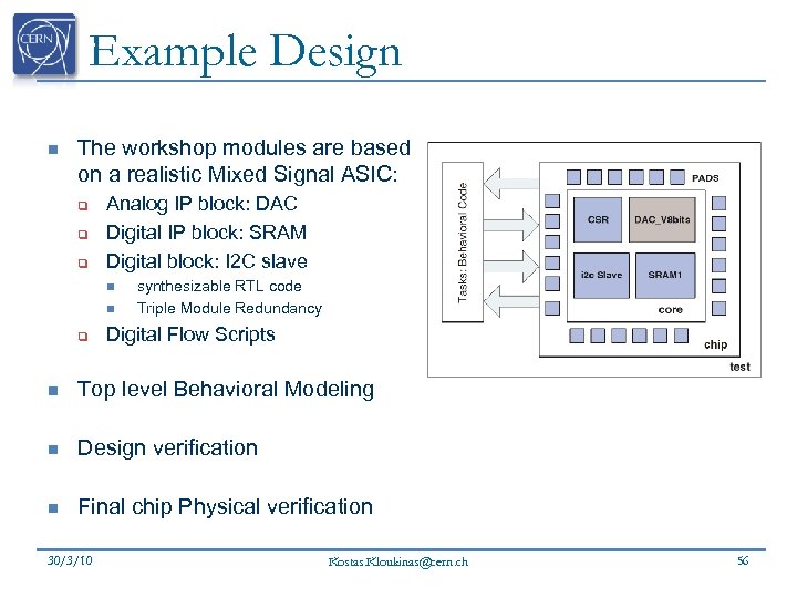 Example Design n The workshop modules are based on a realistic Mixed Signal ASIC: q q q Analog IP block: DAC Digital IP block: SRAM Digital block: I 2 C slave n n q synthesizable RTL code Triple Module Redundancy Digital Flow Scripts n Top level Behavioral Modeling Design verification n Final chip Physical verification n 30/3/10 Kostas. Kloukinas@cern. ch 56
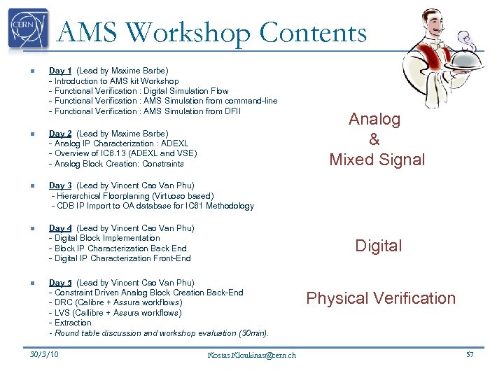 AMS Workshop Contents n Day 1 (Lead by Maxime Barbe) - Introduction to AMS kit Workshop - Functional Verification : Digital Simulation Flow - Functional Verification : AMS Simulation from command-line - Functional Verification : AMS Simulation from DFII n Day 2 (Lead by Maxime Barbe) - Analog IP Characterization : ADEXL - Overview of IC 6. 13 (ADEXL and VSE) - Analog Block Creation: Constraints n Day 3 (Lead by Vincent Cao Van Phu) - Hierarchical Floorplaning (Virtuoso based) - CDB IP Import to OA database for IC 61 Methodology n Day 4 (Lead by Vincent Cao Van Phu) - Digital Block Implementation - Block IP Characterization Back End - Digital IP Characterization Front-End Analog & Mixed Signal n Digital Day 5 (Lead by Vincent Cao Van Phu) - Constraint Driven Analog Block Creation Back-End - DRC (Calibre + Assura workflows) - LVS (Callibre + Assura workflows) - Extraction - Round table discussion and workshop evaluation (30 min). 30/3/10 Kostas. Kloukinas@cern. ch Physical Verification 57
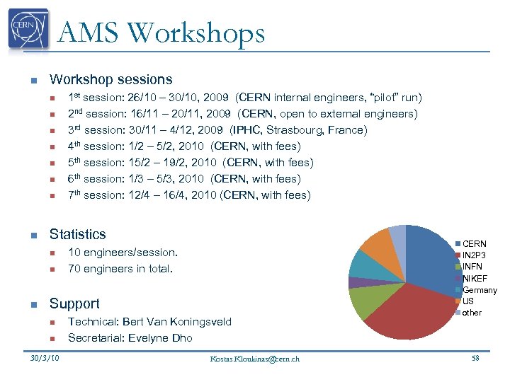 AMS Workshops n Workshop sessions n n n n Statistics n n n 1 st session: 26/10 – 30/10, 2009 (CERN internal engineers, “pilot” run) 2 nd session: 16/11 – 20/11, 2009 (CERN, open to external engineers) 3 rd session: 30/11 – 4/12, 2009 (IPHC, Strasbourg, France) 4 th session: 1/2 – 5/2, 2010 (CERN, with fees) 5 th session: 15/2 – 19/2, 2010 (CERN, with fees) 6 th session: 1/3 – 5/3, 2010 (CERN, with fees) 7 th session: 12/4 – 16/4, 2010 (CERN, with fees) 10 engineers/session. 70 engineers in total. Support n n 30/3/10 Technical: Bert Van Koningsveld Secretarial: Evelyne Dho Kostas. Kloukinas@cern. ch CERN IN 2 P 3 INFN NIKEF Germany US other 58
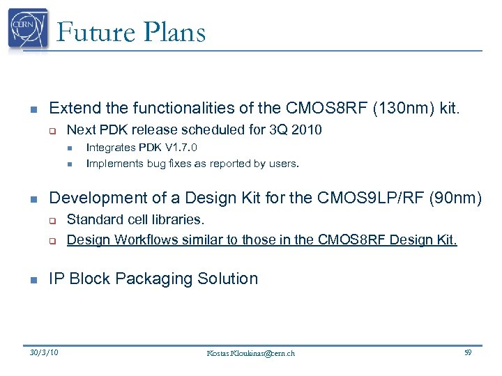 Future Plans n Extend the functionalities of the CMOS 8 RF (130 nm) kit. q Next PDK release scheduled for 3 Q 2010 n n n Development of a Design Kit for the CMOS 9 LP/RF (90 nm) q q n Integrates PDK V 1. 7. 0 Implements bug fixes as reported by users. Standard cell libraries. Design Workflows similar to those in the CMOS 8 RF Design Kit. IP Block Packaging Solution 30/3/10 Kostas. Kloukinas@cern. ch 59
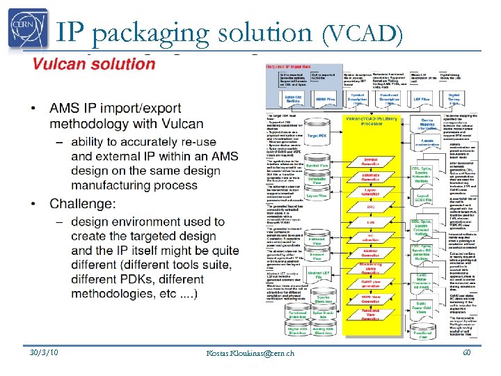 IP packaging solution (VCAD) 30/3/10 Kostas. Kloukinas@cern. ch 60
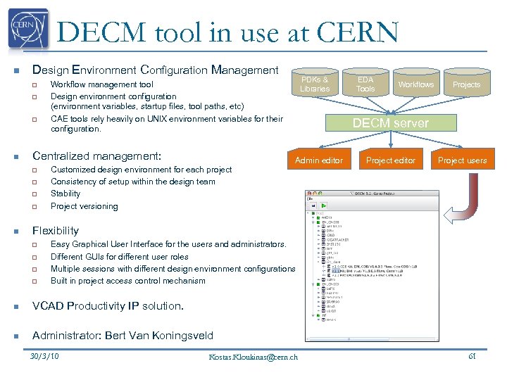 DECM tool in use at CERN n Design Environment Configuration Management q q q n Centralized management: q q n PDKs & Libraries Workflow management tool Design environment configuration (environment variables, startup files, tool paths, etc) CAE tools rely heavily on UNIX environment variables for their configuration. Customized design environment for each project Consistency of setup within the design team Stability Project versioning EDA Tools Workflows Projects DECM server Admin editor Project users Flexibility q q Easy Graphical User Interface for the users and administrators. Different GUIs for different user roles Multiple sessions with different design environment configurations Built in project access control mechanism n VCAD Productivity IP solution. n Administrator: Bert Van Koningsveld 30/3/10 Kostas. Kloukinas@cern. ch 61
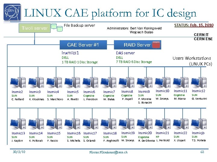 LINUX CAE platform for IC design File Backup server Tivoli server Administrators: Bert Van Koningsveld Wojciech Bialas CAE Server #1 DAS server lnxmic 4 lnxmic 5 lnxmic 13 lnxmic 14 lnxmic 15 lnxmic 16 lnxmic 17 SUN C. Paillard SUN J. Kaplon 30/3/10 SUN K. Kloukinas SUN K. Poltorak SUN S. Marchioro SUN F. Faccio SUN A. Rivetti SUN S. Michelis lnxmic 6 Cogestra L. Pierobon SUN S. Orlandi Users Workstations (LINUX PCs) DELL 7 TB RAID 6 Disc Storage DELL 1 TB RAID 1 Disc Storage lnxmic 3 CERN IT CERN ESE RAID Server lnxmics 1 lnxmic 2 STATUS: Feb. 15, 2010 lnxmic 7 lnxmic 8 Cogestra W. Bialas Cogestra P. Aspell lnxmic 18 lnxmic 19 SUN F. Anghinolfi W. Snoeys Kostas. Kloukinas@cern. ch lnxmic 9 lnxmic 10 lnxmic 11 lnxmic 12 SUN P. Moreira S. Bonacini SUN W. Snoeys lnxmic 20 lnxmic 21 lnxmic 22 lnxmicjb HP Cogestra R. De Oliveira L. Perktold Cogestra M. Marra SUN X. Llopart SUN G. Venturini SUN T. S. Poikela 62
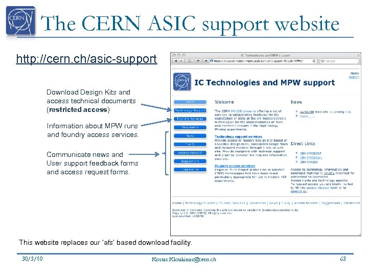 The CERN ASIC support website http: //cern. ch/asic-support Download Design Kits and access technical documents (restricted access) Information about MPW runs and foundry access services. Communicate news and User support feedback forms and access request forms. This website replaces our ‘afs’ based download facility. 30/3/10 Kostas. Kloukinas@cern. ch 63
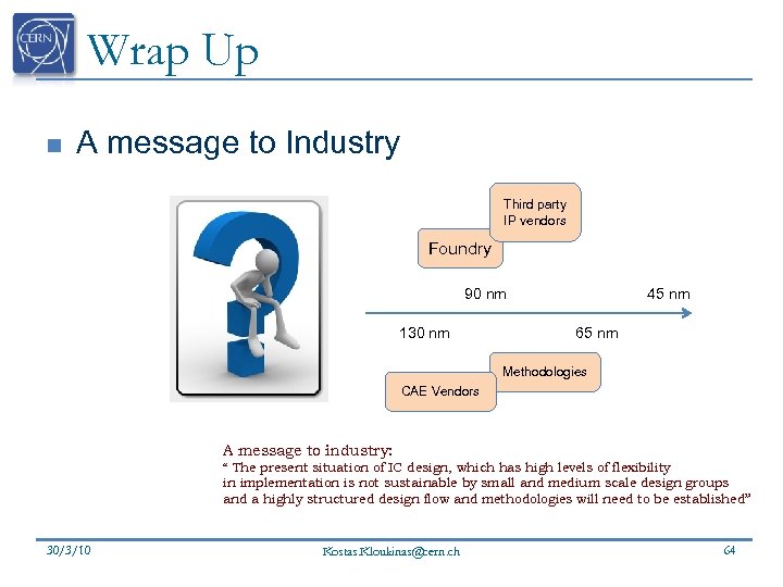 Wrap Up n A message to Industry Third party IP vendors Foundry 90 nm 130 nm 45 nm 65 nm Methodologies CAE Vendors A message to industry: “ The present situation of IC design, which has high levels of flexibility in implementation is not sustainable by small and medium scale design groups and a highly structured design flow and methodologies will need to be established” 30/3/10 Kostas. Kloukinas@cern. ch 64
 THANK YOU Acknowledgements • IDESA training EU 7 th Framework Program (http: //www. idesa-training. org/) for material presented in slides. • Cadence & VCAD services group in Paris for material presented in slides. • IBM for technology data presented in slides. • Sandro Bonacini@CERN. ch, for his work on the customized digital design flow. • Bert. Van. Koningsveld@CERN. ch, Wojciech. Bialas@CERN. ch, for their efforts in the CAE tools support services. 30/3/10 Kostas. Kloukinas@cern. ch 65
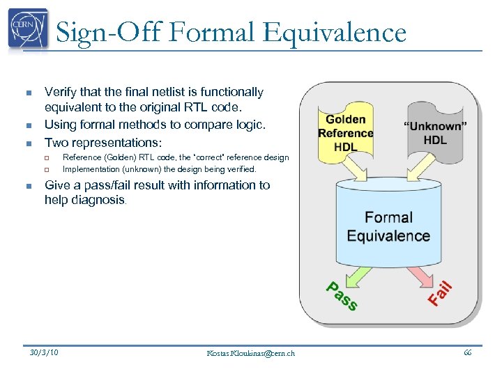 Sign-Off Formal Equivalence n n n Verify that the final netlist is functionally equivalent to the original RTL code. Using formal methods to compare logic. Two representations: q q n Reference (Golden) RTL code, the “correct” reference design Implementation (unknown) the design being verified. Give a pass/fail result with information to help diagnosis. 30/3/10 Kostas. Kloukinas@cern. ch 66


