0495a0553271f6fcfc8efe1b046d6aa5.ppt
- Количество слайдов: 98
 C 2000 Digital Power Supply Workshop Texas Instruments Technical Training D SP TEXAS INSTRUMENTS TECHNOLOGY Copyright © 2008 Texas Instruments. All rights reserved.
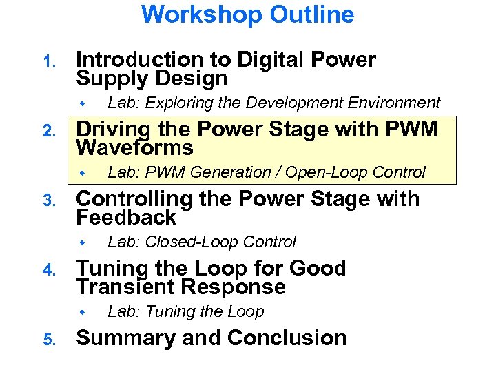
 Workshop Outline 1. Introduction to Digital Power Supply Design 2. Driving the Power Stage with PWM Waveforms 3. Lab: Closed-Loop Control Tuning the Loop for Good Transient Response 5. Lab: PWM Generation / Open-Loop Controlling the Power Stage with Feedback 4. Lab: Exploring the Development Environment Lab: Tuning the Loop Summary and Conclusion
 Workshop Outline 1. Introduction to Digital Power Supply Design 2. Driving the Power Stage with PWM Waveforms 3. Lab: Closed-Loop Control Tuning the Loop for Good Transient Response 5. Lab: PWM Generation / Open-Loop Controlling the Power Stage with Feedback 4. Lab: Exploring the Development Environment Lab: Tuning the Loop Summary and Conclusion
 Introduction to Digital Power Supply Design u u What is a Digital Power Supply? Why use Digital Control Techniques? Peripherals used for Digital Power Supply Design Development Tools and Software
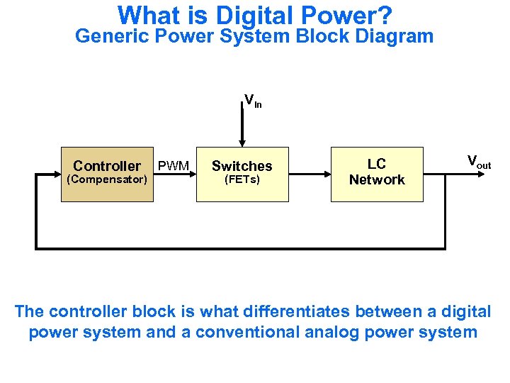 What is Digital Power? Generic Power System Block Diagram Vin Controller (Compensator) PWM Switches (FETs) LC Network Vout The controller block is what differentiates between a digital power system and a conventional analog power system
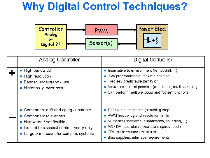 Why Digital Control Techniques? Controller Analog or Digital ? ? PWM Sensor(s) Analog Controller + Power Elec. Digital Controller High bandwidth u High resolution u Easy to understand / use u Historically lower cost u Insensitive to environment (temp, drift, …) Component drift and aging / unstable u Component tolerances u Hardwired / not flexible u Limited to classical control theory only u Large parts count for complex systems u Bandwidth limitations (sampling loop) u u S/w programmable / flexible solution u Precise / predictable behavior u Advanced control possible (non-linear, multi-variable) u Can perform multiple loops and “other” functions u PWM frequency and resolution limits u Numerical problems (quantization, rounding, …) u AD / DA boundary (resolution, speed, cost) u CPU performance limitations u Bias supplies, interface requirements u
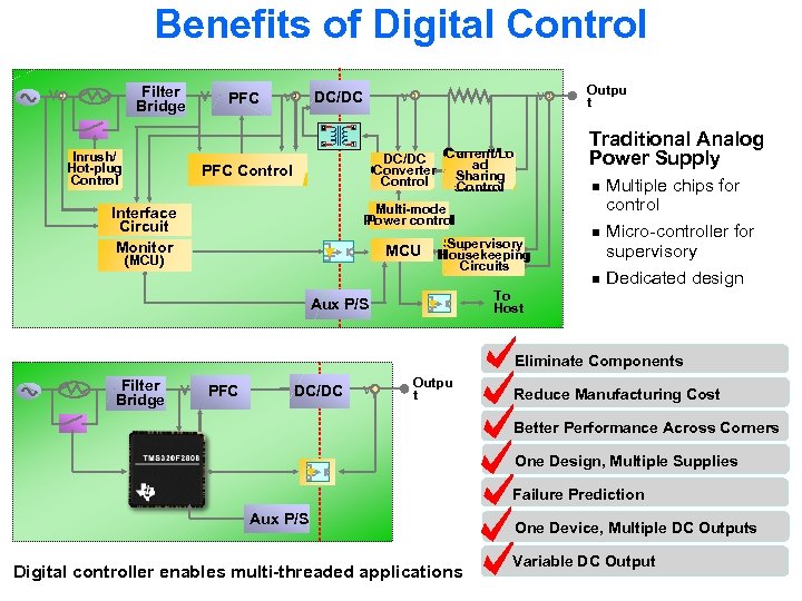 Benefits of Digital Control Filter V Bridge VI PFC VI DC/DC 8 Inrush/ Hot-plug Control 1 V I 4 5 V n Multi-mode Power control Interface Circuit Monitor MCU (MCU) (MCU? ) Outpu t Traditional Analog Power Supply Current/Lo DC/DC ad ad Converter Sharing Control PFC Control I Supervisory Housekeeping Circuits Multiple chips for control n Micro-controller for supervisory Dedicated design n To Host Aux P/S Eliminate Components Filter V Bridge PFC DC/DC V Outpu t Reduce Manufacturing Cost Better Performance Across Corners One Design, Multiple Supplies Failure Prediction Aux P/S Digital controller enables multi-threaded applications One Device, Multiple DC Outputs Variable DC Output
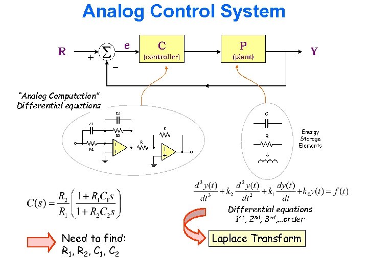 Analog Control System “Analog Computation” Differential equations 1 st, 2 nd, 3 rd, …order Need to find: R 1, R 2, C 1, C 2 Laplace Transform
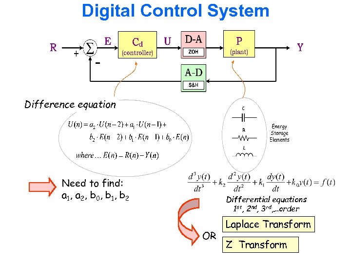 Digital Control System Difference equation Need to find: a 1, a 2, b 0, b 1, b 2 Differential equations 1 st, 2 nd, 3 rd, …order OR Laplace Transform Z Transform
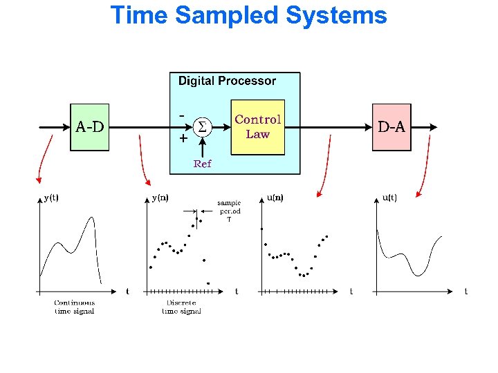 Time Sampled Systems
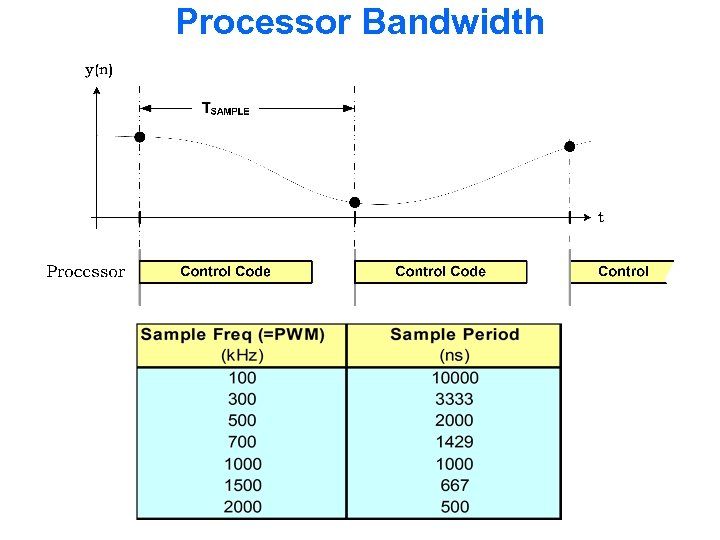 Processor Bandwidth
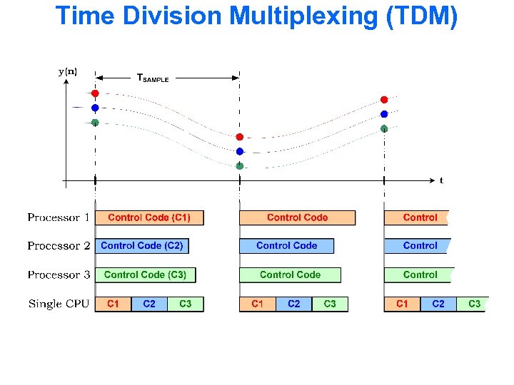 Time Division Multiplexing (TDM)
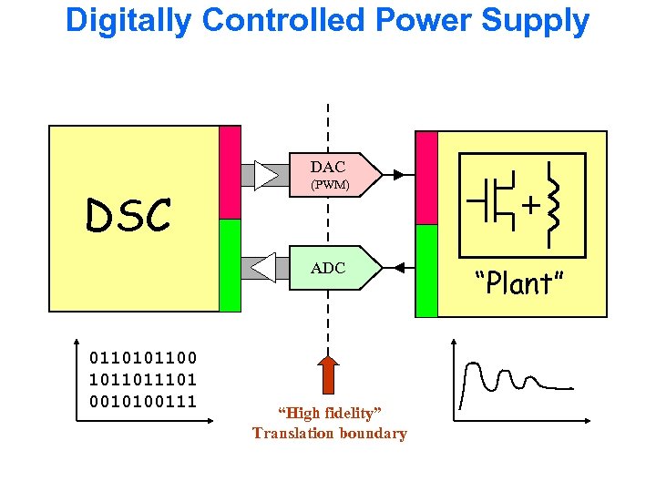 Digitally Controlled Power Supply DAC DSC (PWM) ADC 0110101100 101101 0010100111 “High fidelity” Translation boundary “Plant”
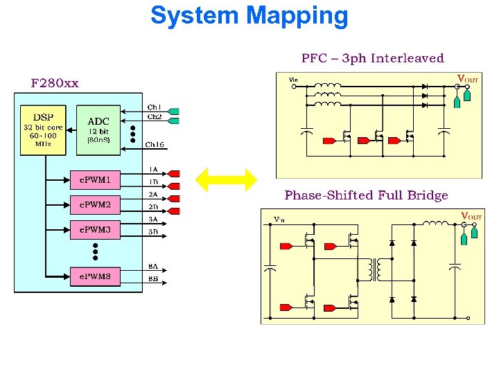 System Mapping
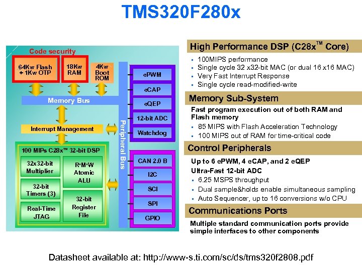 TMS 320 F 280 x High Performance DSP (C 28 x Code security § 64 Kw Flash + 1 Kw OTP 18 Kw RAM 4 Kw Boot ROM § e. PWM e. CAP Memory Bus 100 MIPs C 28 x. TM 32 -bit DSP 32 x 32 -bit Multiplier 32 -bit Timers (3) Real-Time JTAG R M W Atomic ALU Peripheral Bus Interrupt Management e. QEP 12 -bit ADC Watchdog § Core) 100 MIPS performance Single cycle 32 x 32 -bit MAC (or dual 16 x 16 MAC) Very Fast Interrupt Response Single cycle read-modified-write Memory Sub-System Fast program execution out of both RAM and Flash memory § 85 MIPS with Flash Acceleration Technology § 100 MIPS out of RAM for time-critical code Control Peripherals CAN 2. 0 B I 2 C SCI 32 -bit Register File § TM SPI GPIO Up to 6 e. PWM, 4 e. CAP, and 2 e. QEP Ultra-Fast 12 -bit ADC § 6. 25 MSPS throughput § Dual sample&holds enable simultaneous sampling § Auto Sequencer, up to 16 conversions w/o CPU Communications Ports Multiple standard communication ports provide simple interfaces to other components Datasheet available at: http: //www-s. ti. com/sc/ds/tms 320 f 2808. pdf
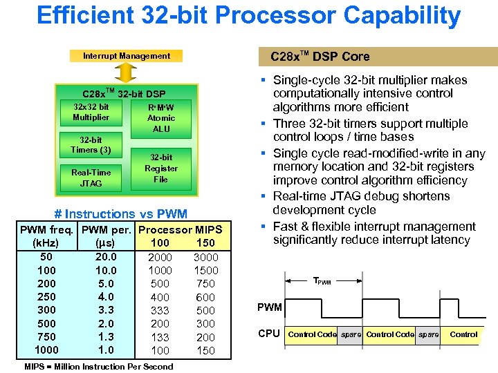 Efficient 32 -bit Processor Capability Interrupt Management C 28 x TM 32 x 32 bit Multiplier 32 -bit Timers (3) Real-Time JTAG 32 -bit DSP R M W Atomic ALU 32 -bit Register File # Instructions vs PWM freq. PWM per. Processor MIPS (k. Hz) ( s) 100 150 50 2000 3000 1000 1500 200 5. 0 500 750 250 4. 0 400 600 3. 3 333 500 2. 0 200 300 750 1. 3 133 200 1000 1. 0 100 150 MIPS = Million Instruction Per Second C 28 x. TM DSP Core § Single-cycle 32 -bit multiplier makes computationally intensive control algorithms more efficient § Three 32 -bit timers support multiple control loops / time bases § Single cycle read-modified-write in any memory location and 32 -bit registers improve control algorithm efficiency § Real-time JTAG debug shortens development cycle § Fast & flexible interrupt management significantly reduce interrupt latency TPWM CPU Control Code spare Control
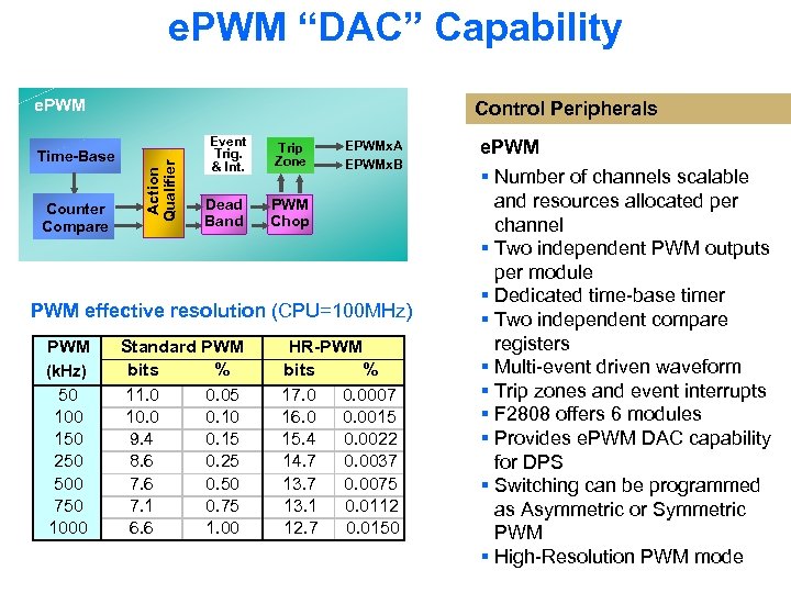 e. PWM “DAC” Capability e. PWM Counter Compare Action Qualifier Time-Base Control Peripherals Event Trig. & Int. Trip Zone Dead Band PWM Chop EPWMx. A EPWMx. B PWM effective resolution (CPU=100 MHz) PWM (k. Hz) 50 100 150 250 500 750 1000 Standard PWM bits % 11. 0 0. 05 10. 0 0. 10 9. 4 0. 15 8. 6 0. 25 7. 6 0. 50 7. 1 0. 75 6. 6 1. 00 HR-PWM bits % 17. 0 0. 0007 16. 0 0. 0015 15. 4 0. 0022 14. 7 0. 0037 13. 7 0. 0075 13. 1 0. 0112 12. 7 0. 0150 e. PWM § Number of channels scalable and resources allocated per channel § Two independent PWM outputs per module § Dedicated time-base timer § Two independent compare registers § Multi-event driven waveform § Trip zones and event interrupts § F 2808 offers 6 modules § Provides e. PWM DAC capability for DPS § Switching can be programmed as Asymmetric or Symmetric PWM § High-Resolution PWM mode
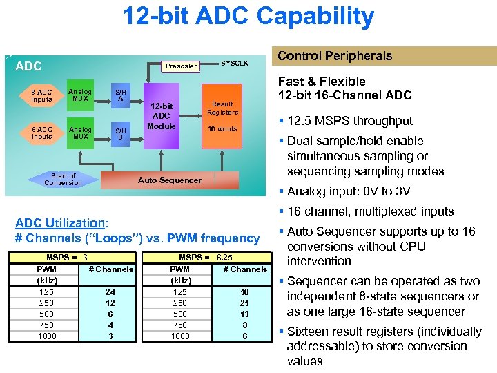 12 -bit ADC Capability ADC Prescaler 8 ADC Inputs Analog MUX S/H A 8 ADC Inputs Analog MUX S/H B Start of Conversion 12 -bit ADC Module SYSCLK Result Registers 16 words Auto Sequencer ADC Utilization: # Channels (“Loops”) vs. PWM frequency MSPS = 3 PWM # Channels (k. Hz) 125 24 250 12 500 6 750 4 1000 3 MSPS = 6. 25 PWM # Channels (k. Hz) 125 500 13 750 8 1000 6 Control Peripherals Fast & Flexible 12 -bit 16 -Channel ADC § 12. 5 MSPS throughput § Dual sample/hold enable simultaneous sampling or sequencing sampling modes § Analog input: 0 V to 3 V § 16 channel, multiplexed inputs § Auto Sequencer supports up to 16 conversions without CPU intervention § Sequencer can be operated as two independent 8 -state sequencers or as one large 16 -state sequencer § Sixteen result registers (individually addressable) to store conversion values
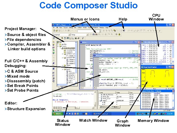 Code Composer Studio Menus or Icons Help CPU Window Project Manager: ØSource & object files ØFile dependencies ØCompiler, Assembler & Linker build options Full C/C++ & Assembly Debugging: ØC & ASM Source ØMixed mode ØDisassembly (patch) ØSet Break Points ØSet Probe Points Editor: ØStructure Expansion Status Window Watch Window Graph Window Memory Window
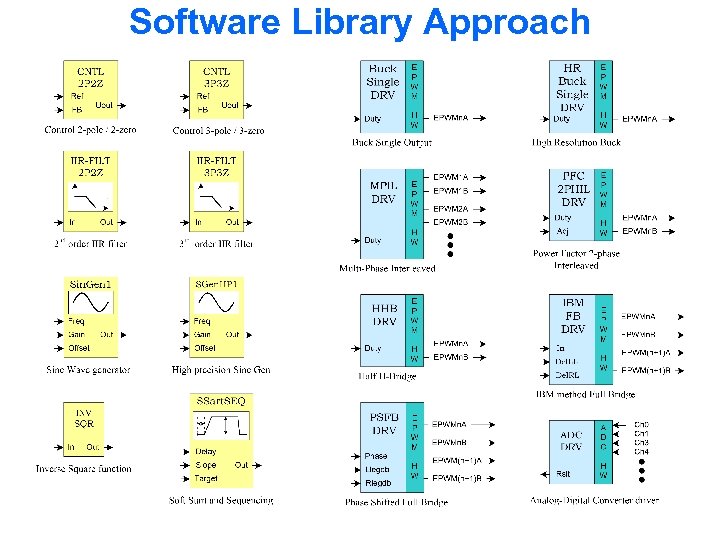 Software Library Approach
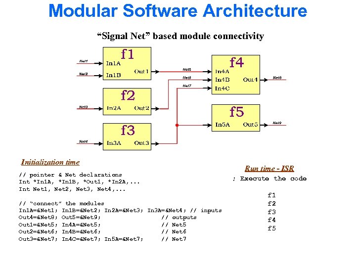 Modular Software Architecture “Signal Net” based module connectivity Initialization time // pointer & Net declarations Int *In 1 A, *In 1 B, *Out 1, *In 2 A, . . . Int Net 1, Net 2, Net 3, Net 4, . . . // “connect” the modules In 1 A=&Net 1; In 1 B=&Net 2; In 2 A=&Net 3; In 3 A=&Net 4; // inputs Out 4=&Net 8; Out 5=&Net 9; // outputs Out 1=&Net 5; In 4 A=&Net 5; // Net 5 Out 2=&Net 6; In 4 B=&Net 6; // Net 6 Out 3=&Net 7; In 4 C=&Net 7; In 5 A=&Net 7; // Net 7 Run time - ISR ; Execute the code f 1 f 2 f 3 f 4 f 5
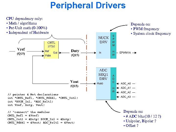 Peripheral Drivers CPU dependency only: • Math / algorithms • Per-Unit math (0 -100%) • Independent of Hardware Depends on: • PWM frequency • System clock frequency // pointer & Net declarations int *CNTL_Ref 1, *CNTL_Fdbk 1, *CNTL_Out 1; int *BUCK_In 1, *ADC_Rslt 1; int Vref, Duty, Vout; // “connect” the modules CNTL_Ref 1 = &Vref; CNTL_Out 1 = &Duty; BUCK_In 1 = &Duty; CNTL_Fdbk 1 = &Vout; ADC_Rslt 1 = &Vout; Depends on: • # ADC bits (10 / 12 ? ) • Unipolar, Bipolar ? • Offset ?
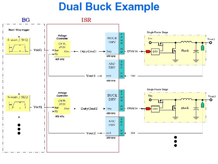 Dual Buck Example
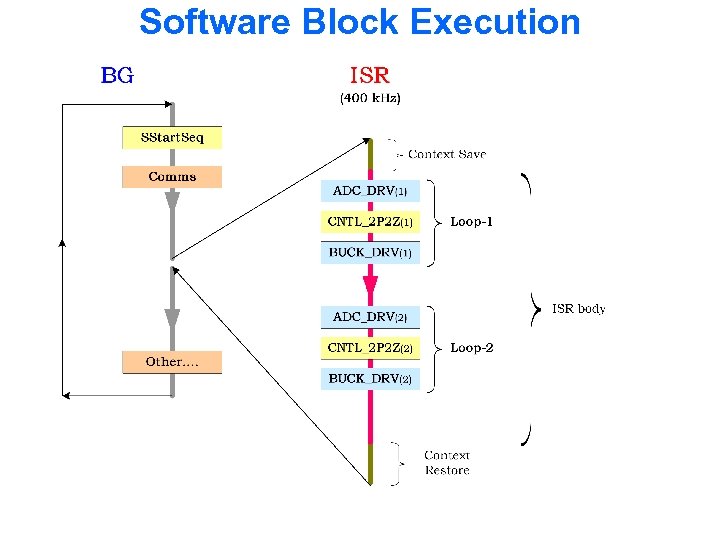 Software Block Execution
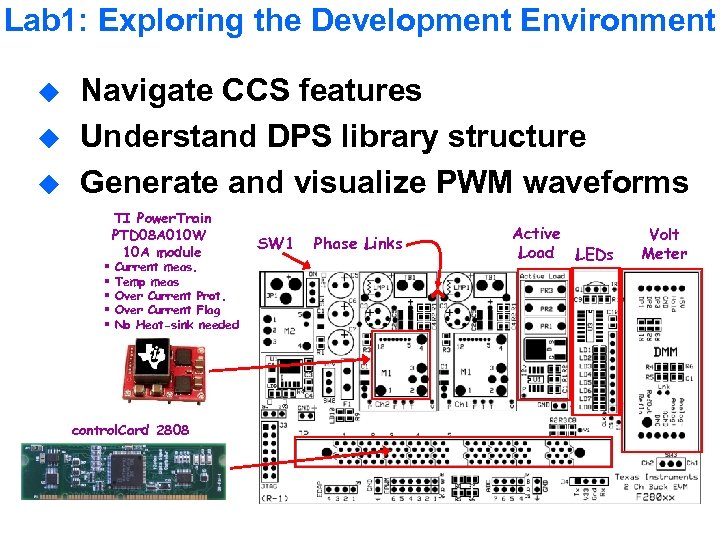 Lab 1: Exploring the Development Environment u u u Navigate CCS features Understand DPS library structure Generate and visualize PWM waveforms § § § TI Power. Train PTD 08 A 010 W 10 A module Current meas. Temp meas Over Current Prot. Over Current Flag No Heat-sink needed control. Card 2808 SW 1 Phase Links Active Load LEDs Volt Meter
 Workshop Outline 1. Introduction to Digital Power Supply Design 2. Driving the Power Stage with PWM Waveforms 3. Lab: Closed-Loop Control Tuning the Loop for Good Transient Response 5. Lab: PWM Generation / Open-Loop Controlling the Power Stage with Feedback 4. Lab: Exploring the Development Environment Lab: Tuning the Loop Summary and Conclusion
 Driving the Power Stage with PWM Waveforms u u u Open-Loop System Block Diagram Generating PWM using the e. PWM Module Power Stage Topologies and Software Library Support
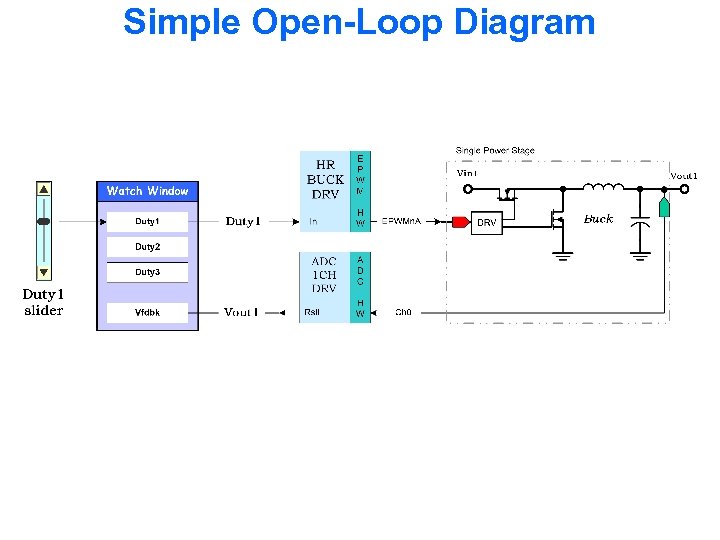 Simple Open-Loop Diagram
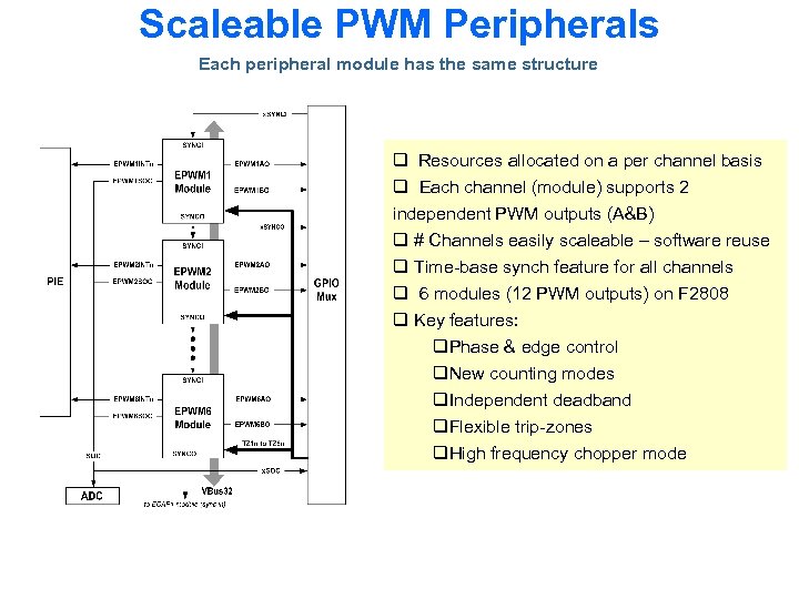 Scaleable PWM Peripherals Each peripheral module has the same structure q Resources allocated on a per channel basis q Each channel (module) supports 2 independent PWM outputs (A&B) q # Channels easily scaleable – software reuse q Time-base synch feature for all channels q 6 modules (12 PWM outputs) on F 2808 q Key features: q. Phase & edge control q. New counting modes q. Independent deadband q. Flexible trip-zones q. High frequency chopper mode
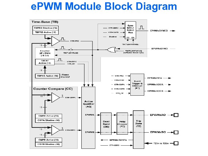 e. PWM Module Block Diagram
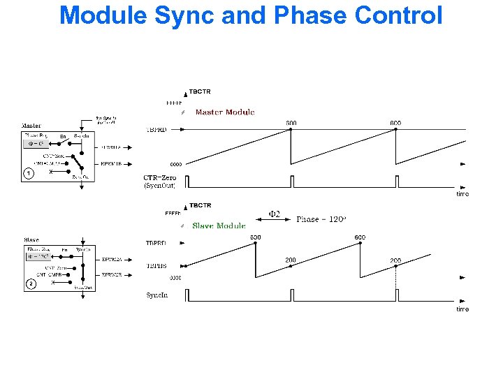 Module Sync and Phase Control
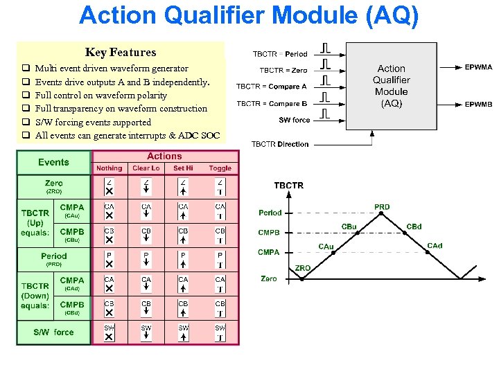 Action Qualifier Module (AQ) Key Features q q q Multi event driven waveform generator Events drive outputs A and B independently. Full control on waveform polarity Full transparency on waveform construction S/W forcing events supported All events can generate interrupts & ADC SOC
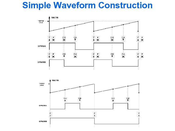 Simple Waveform Construction
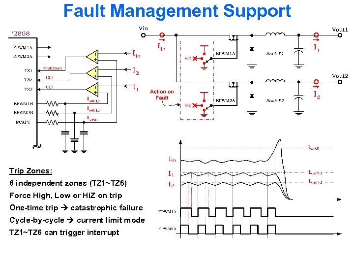 Fault Management Support Trip Zones: 6 independent zones (TZ 1~TZ 6) Force High, Low or Hi. Z on trip One-time trip catastrophic failure Cycle-by-cycle current limit mode TZ 1~TZ 6 can trigger interrupt
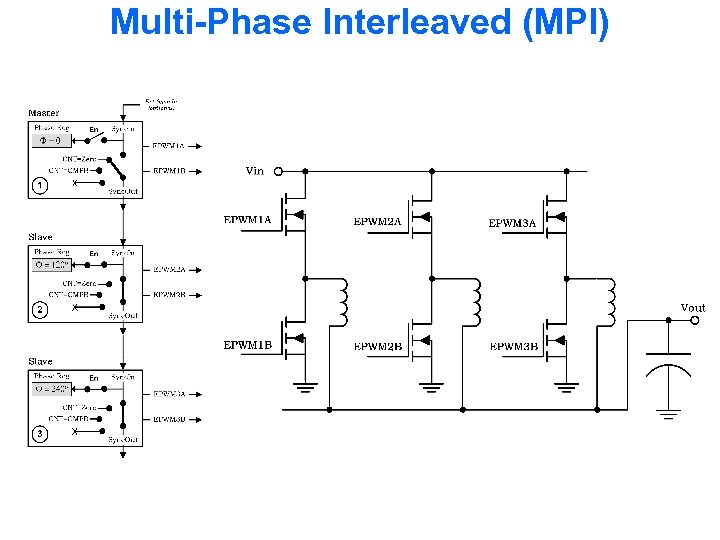 Multi-Phase Interleaved (MPI)
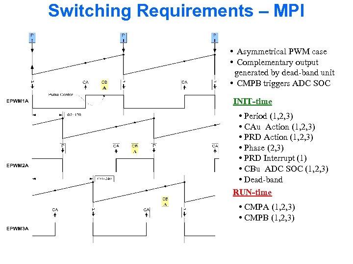 Switching Requirements – MPI • Asymmetrical PWM case • Complementary output generated by dead-band unit • CMPB triggers ADC SOC INIT-time • Period (1, 2, 3) • CAu Action (1, 2, 3) • PRD Action (1, 2, 3) • Phase (2, 3) • PRD Interrupt (1) • CBu ADC SOC (1, 2, 3) • Dead-band RUN-time • CMPA (1, 2, 3) • CMPB (1, 2, 3)
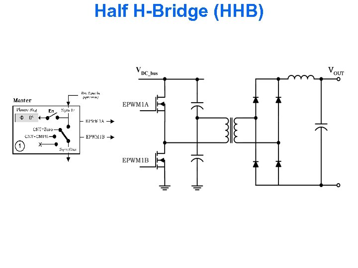 Half H-Bridge (HHB)
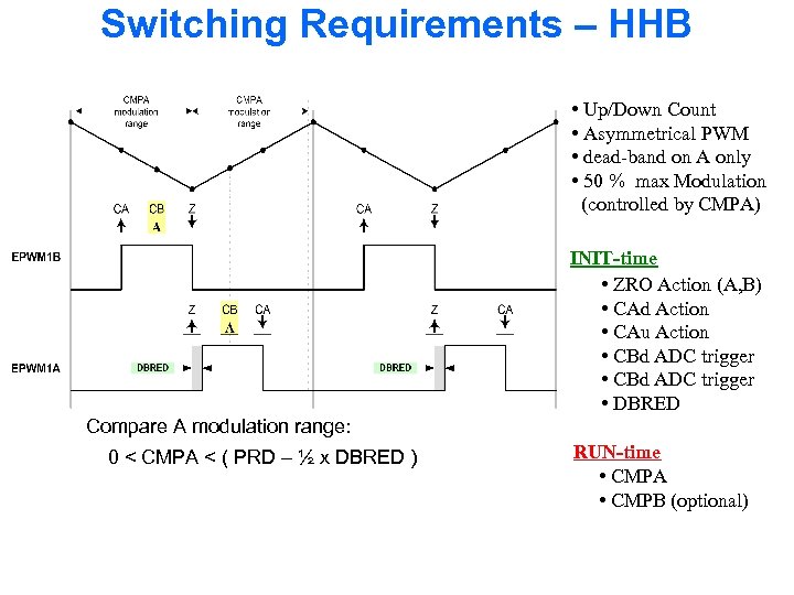 Switching Requirements – HHB • Up/Down Count • Asymmetrical PWM • dead-band on A only • 50 % max Modulation (controlled by CMPA) INIT-time • ZRO Action (A, B) • CAd Action • CAu Action • CBd ADC trigger • DBRED Compare A modulation range: 0 < CMPA < ( PRD – ½ x DBRED ) RUN-time • CMPA • CMPB (optional)
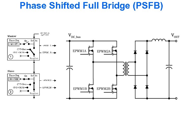 Phase Shifted Full Bridge (PSFB)
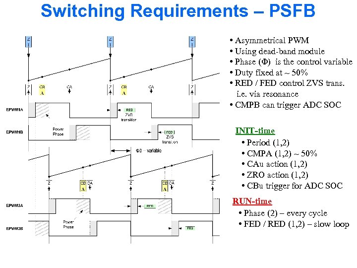 Switching Requirements – PSFB • Asymmetrical PWM • Using dead-band module • Phase (Φ) is the control variable • Duty fixed at ~ 50% • RED / FED control ZVS trans. i. e. via resonance • CMPB can trigger ADC SOC INIT-time • Period (1, 2) • CMPA (1, 2) ~ 50% • CAu action (1, 2) • ZRO action (1, 2) • CBu trigger for ADC SOC RUN-time • Phase (2) – every cycle • FED / RED (1, 2) – slow loop
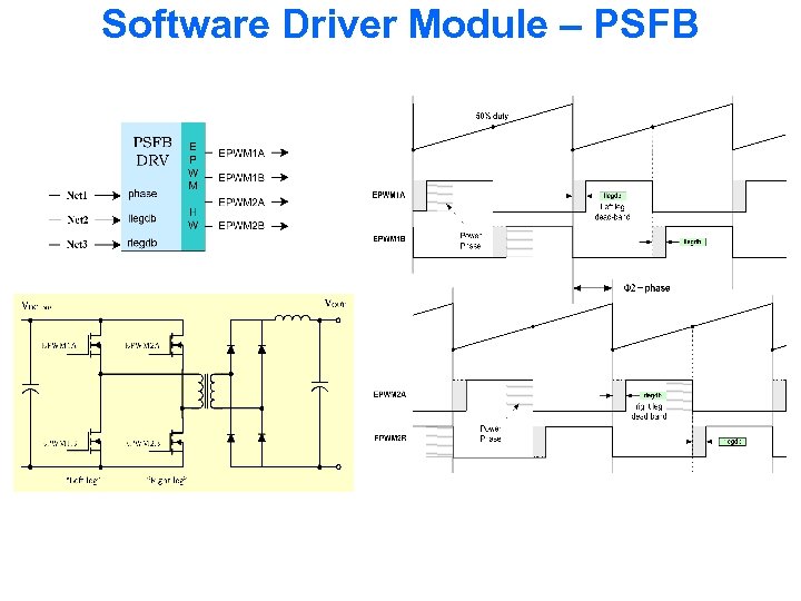 Software Driver Module – PSFB
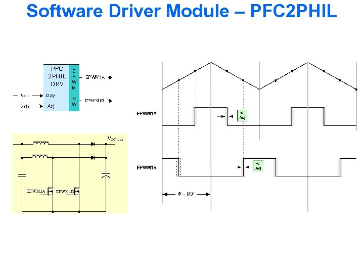 Software Driver Module – PFC 2 PHIL
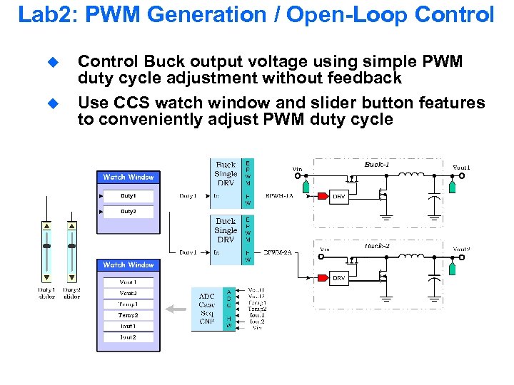 Lab 2: PWM Generation / Open-Loop Control u u Control Buck output voltage using simple PWM duty cycle adjustment without feedback Use CCS watch window and slider button features to conveniently adjust PWM duty cycle
 Workshop Outline 1. Introduction to Digital Power Supply Design 2. Driving the Power Stage with PWM Waveforms 3. Lab: Closed-Loop Control Tuning the Loop for Good Transient Response 5. Lab: PWM Generation / Open-Loop Controlling the Power Stage with Feedback 4. Lab: Exploring the Development Environment Lab: Tuning the Loop Summary and Conclusion
 Controlling the Power Stage with Feedback u u u Closed-Loop System Block Diagram Analog-to-Digital Converter Module Digital Control of Power Converter High Resolution PWM Benefits Soft Start – Starting the Loop
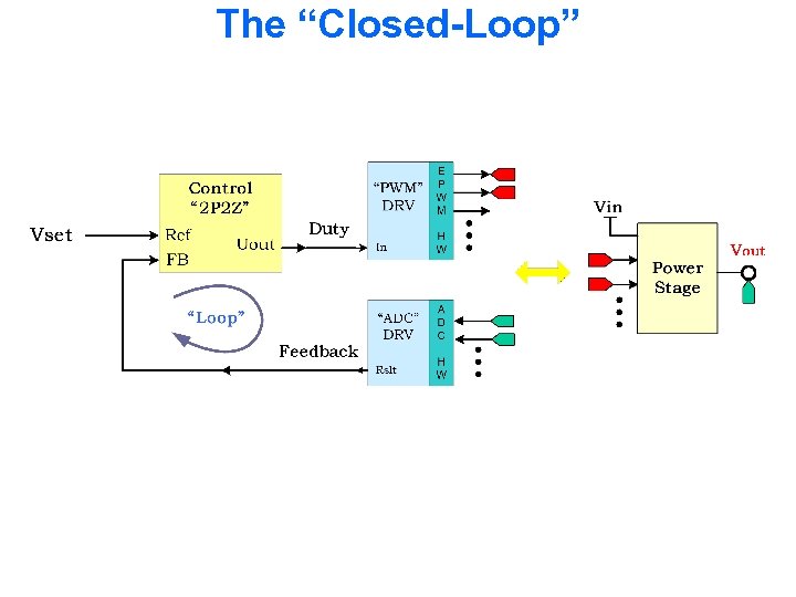 The “Closed-Loop”
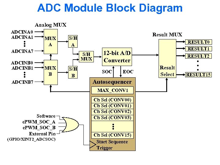 ADC Module Block Diagram Analog MUX . . . MUX A ADCINA 7 ADCINB 0 ADCINB 1 Result MUX S/H A S/H MUX . . . MUX B ADCINB 7 S/H B 12 -bit A/D Converter SOC EOC Autosequencer MAX_CONV 1 (GPIO/XINT 2_ADCSOC) Ch Sel (CONV 00) Ch Sel (CONV 01) Ch Sel (CONV 02) Ch Sel (CONV 03) . . . Software e. PWM_SOC_A e. PWM_SOC_B External Pin RESULT 0 RESULT 1 RESULT 2 Ch Sel (CONV 15) Start Sequence Trigger Result Select . . . ADCINA 0 ADCINA 1 RESULT 15
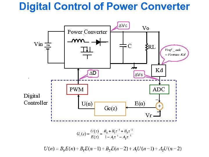 Digital Control of Power Converter Vc Vo Power Converter Vin C D Digital Controller RL Kd Vs PWM U(n) ADC Gc(z) E(n) + Vr +
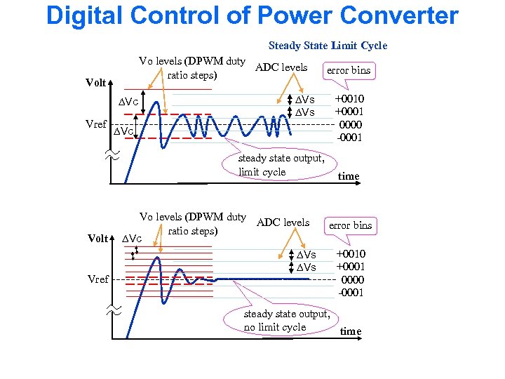 Digital Control of Power Converter Steady State Limit Cycle Vo levels (DPWM duty ADC levels ratio steps) Volt Vc Vref Vs Vs Vc steady state output, limit cycle Volt Vref Vo levels (DPWM duty ADC levels ratio steps) Vc Vs Vs error bins +0010 +0001 0000 -0001 time error bins +0010 +0001 0000 -0001 steady state output, no limit cycle time
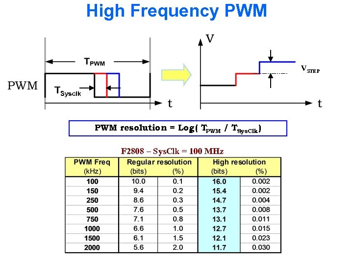 High Frequency PWM VSTEP TSysclk PWM resolution = Log ( TPWM / TSys. Clk ) 2 F 2808 – Sys. Clk = 100 MHz
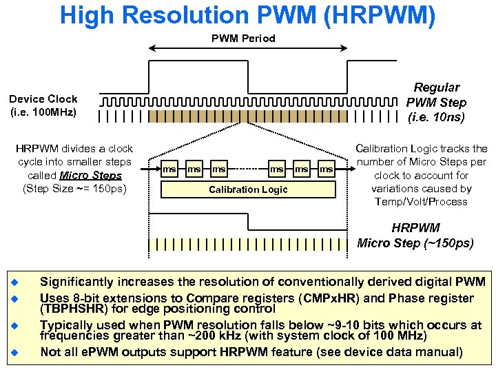 High Resolution PWM (HRPWM) PWM Period Regular PWM Step (i. e. 10 ns) Device Clock (i. e. 100 MHz) HRPWM divides a clock cycle into smaller steps called Micro Steps (Step Size ~= 150 ps) ms ms Calibration Logic tracks the number of Micro Steps per clock to account for variations caused by Temp/Volt/Process HRPWM Micro Step (~150 ps) u u Significantly increases the resolution of conventionally derived digital PWM Uses 8 -bit extensions to Compare registers (CMPx. HR) and Phase register (TBPHSHR) for edge positioning control Typically used when PWM resolution falls below ~9 -10 bits which occurs at frequencies greater than ~200 k. Hz (with system clock of 100 MHz) Not all e. PWM outputs support HRPWM feature (see device data manual)
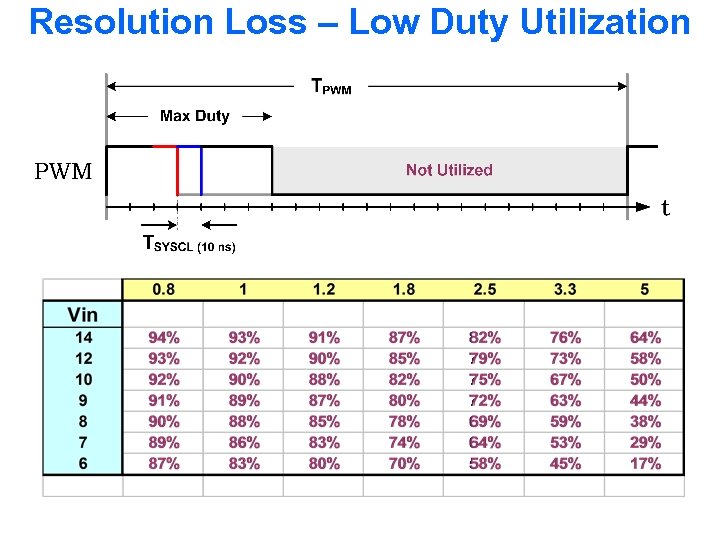 Resolution Loss – Low Duty Utilization
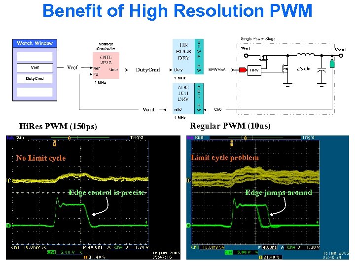 Benefit of High Resolution PWM Hi. Res PWM (150 ps) Regular PWM (10 ns) Limit cycle problem No Limit cycle Edge control is precise Edge jumps around
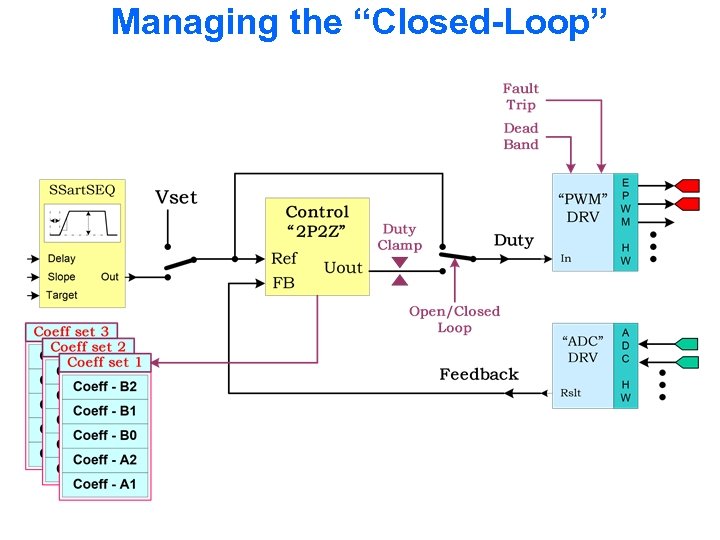 Managing the “Closed-Loop”
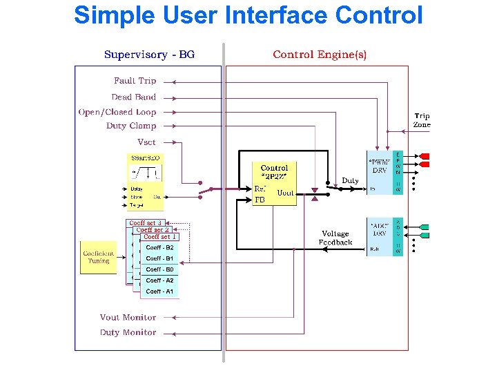 Simple User Interface Control
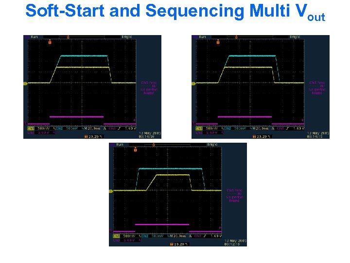 Soft-Start and Sequencing Multi Vout
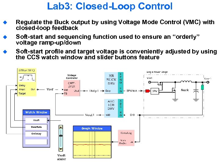 Lab 3: Closed-Loop Control u u u Regulate the Buck output by using Voltage Mode Control (VMC) with closed-loop feedback Soft-start and sequencing function used to ensure an “orderly” voltage ramp-up/down Soft-start profile and target voltage is conveniently adjusted by using the CCS watch window and slider buttons feature
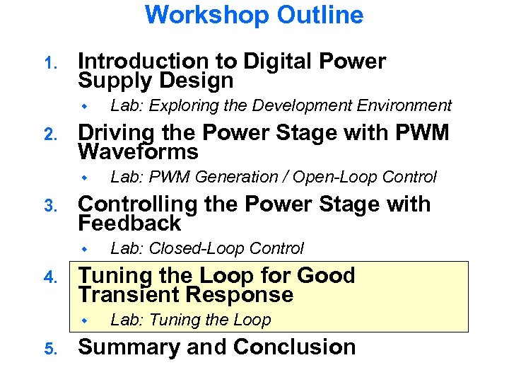 Workshop Outline 1. Introduction to Digital Power Supply Design 2. Driving the Power Stage with PWM Waveforms 3. Lab: Closed-Loop Control Tuning the Loop for Good Transient Response 5. Lab: PWM Generation / Open-Loop Controlling the Power Stage with Feedback 4. Lab: Exploring the Development Environment Lab: Tuning the Loop Summary and Conclusion
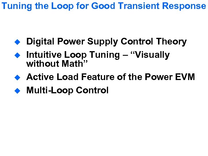 Tuning the Loop for Good Transient Response u u Digital Power Supply Control Theory Intuitive Loop Tuning – “Visually without Math” Active Load Feature of the Power EVM Multi-Loop Control
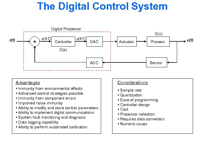 The Digital Control System Digital Processor G(s) r(t) + e(k. T) Controller u(k. T) DAC Actuator Process D(z) ADC Sensor Advantages Considerations • Immunity from environmental effects • Advanced control strategies possible • Immunity from component errors • Improved noise immunity • Ability to modify and store control parameters • Ability to implement digital communications • System fault monitoring and diagnosis • Data logging capability • Ability to perform automated calibration • Sample rate • Quantization • Ease of programming • Controller design • Cost • Processor selection • Requires data converters • Numeric issues c(t)
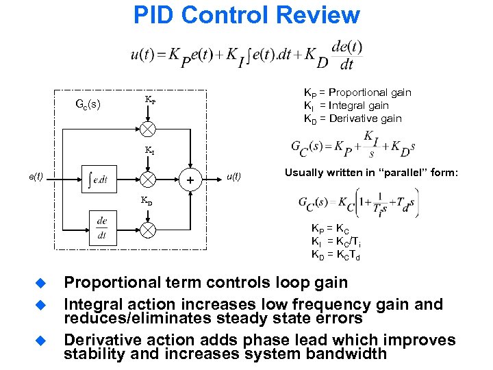 PID Control Review Gc(s) KP = Proportional gain KI = Integral gain KD = Derivative gain KP KI e(t) + u(t) Usually written in “parallel” form: KD KP = K C KI = KC/Ti K D = K CT d u u u Proportional term controls loop gain Integral action increases low frequency gain and reduces/eliminates steady state errors Derivative action adds phase lead which improves stability and increases system bandwidth
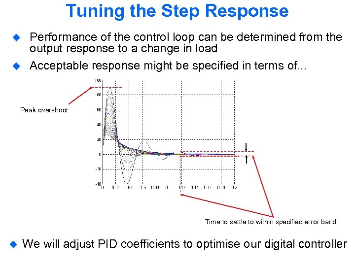 Tuning the Step Response u u Performance of the control loop can be determined from the output response to a change in load Acceptable response might be specified in terms of. . . Peak overshoot Time to settle to within specified error band u We will adjust PID coefficients to optimise our digital controller
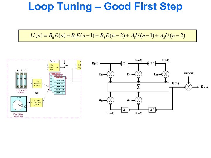 Loop Tuning – Good First Step
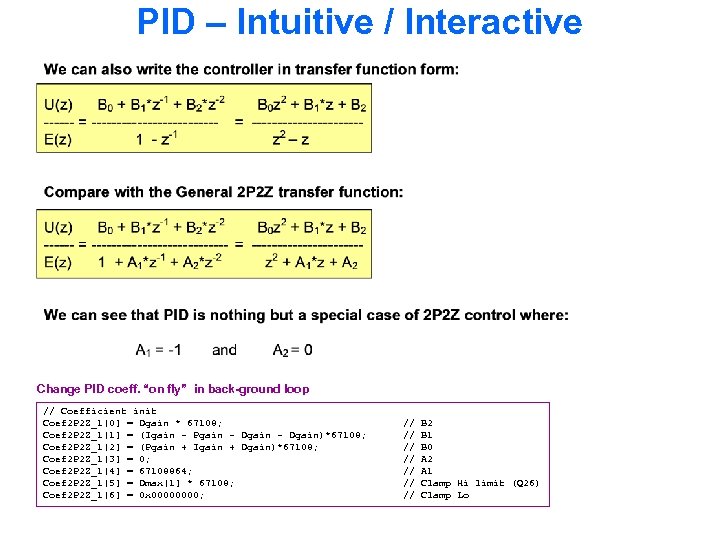 PID – Intuitive / Interactive Change PID coeff. “on fly” in back-ground loop // Coefficient init Coef 2 P 2 Z_1[0] = Dgain * 67108; Coef 2 P 2 Z_1[1] = (Igain - Pgain - Dgain)*67108; Coef 2 P 2 Z_1[2] = (Pgain + Igain + Dgain)*67108; Coef 2 P 2 Z_1[3] = 0; Coef 2 P 2 Z_1[4] = 67108864; Coef 2 P 2 Z_1[5] = Dmax[1] * 67108; Coef 2 P 2 Z_1[6] = 0 x 0000; // // B 2 B 1 B 0 A 2 A 1 Clamp Hi limit (Q 26) Clamp Lo
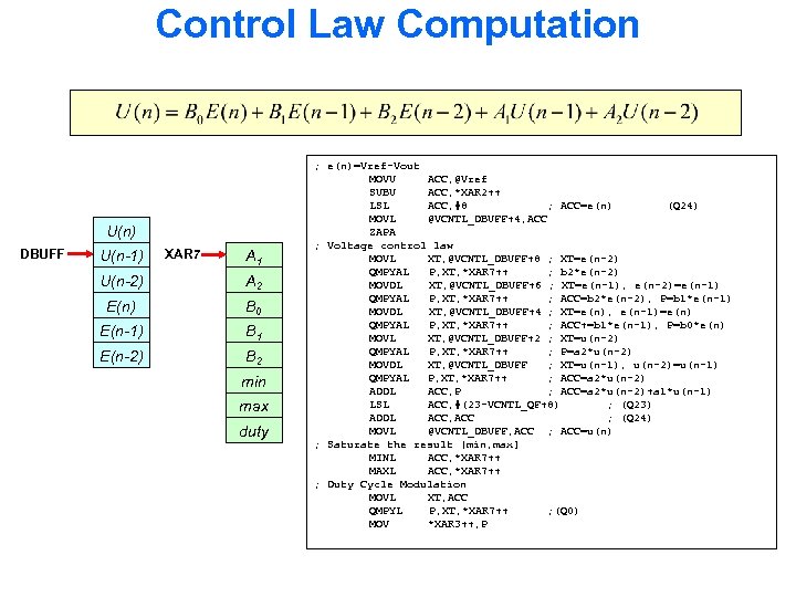 Control Law Computation U(n) DBUFF U(n-1) XAR 7 A 1 U(n-2) A 2 E(n) B 0 E(n-1) B 1 E(n-2) B 2 min max duty ; e(n)=Vref-Vout MOVU ACC, @Vref SUBU ACC, *XAR 2++ LSL ACC, #8 ; ACC=e(n) (Q 24) MOVL @VCNTL_DBUFF+4, ACC ZAPA ; Voltage control law MOVL XT, @VCNTL_DBUFF+8 ; XT=e(n-2) QMPYAL P, XT, *XAR 7++ ; b 2*e(n-2) MOVDL XT, @VCNTL_DBUFF+6 ; XT=e(n-1), e(n-2)=e(n-1) QMPYAL P, XT, *XAR 7++ ; ACC=b 2*e(n-2), P=b 1*e(n-1) MOVDL XT, @VCNTL_DBUFF+4 ; XT=e(n), e(n-1)=e(n) QMPYAL P, XT, *XAR 7++ ; ACC+=b 1*e(n-1), P=b 0*e(n) MOVL XT, @VCNTL_DBUFF+2 ; XT=u(n-2) QMPYAL P, XT, *XAR 7++ ; P=a 2*u(n-2) MOVDL XT, @VCNTL_DBUFF ; XT=u(n-1), u(n-2)=u(n-1) QMPYAL P, XT, *XAR 7++ ; ACC=a 2*u(n-2) ADDL ACC, P ; ACC=a 2*u(n-2)+a 1*u(n-1) LSL ACC, #(23 -VCNTL_QF+8) ; (Q 23) ADDL ACC, ACC ; (Q 24) MOVL @VCNTL_DBUFF, ACC ; ACC=u(n) ; Saturate the result [min, max] MINL ACC, *XAR 7++ MAXL ACC, *XAR 7++ ; Duty Cycle Modulation MOVL XT, ACC QMPYL P, XT, *XAR 7++ ; (Q 0) MOV *XAR 3++, P
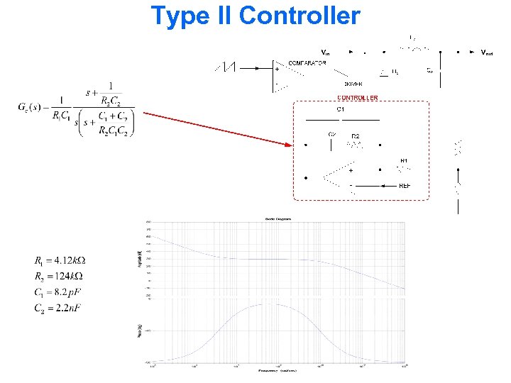 Type II Controller
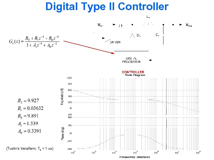 Digital Type II Controller (Tustin’s transform, Ts = 1 us)
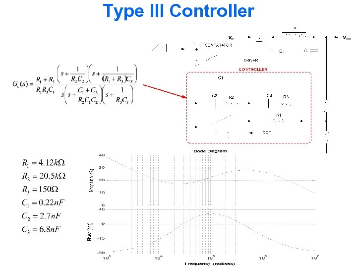 Type III Controller
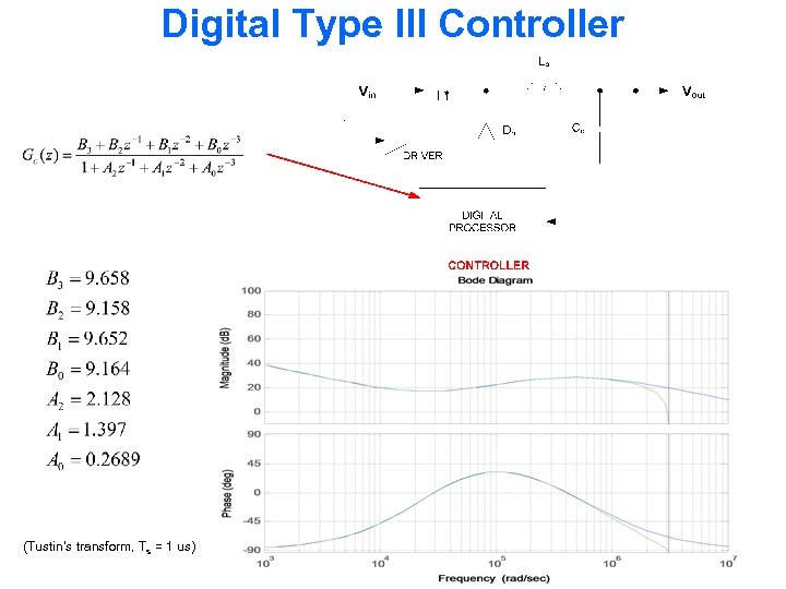 Digital Type III Controller (Tustin’s transform, Ts = 1 us)
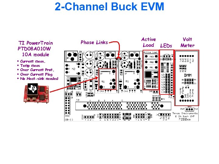 2 -Channel Buck EVM TI Power. Train PTD 08 A 010 W 10 A module § § § Current meas. Temp meas Over Current Prot. Over Current Flag No Heat-sink needed Phase Links Active Load LEDs Volt Meter
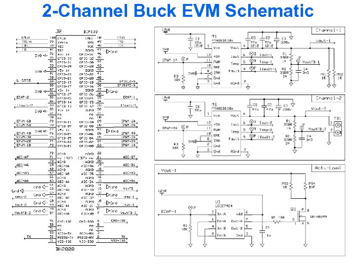 2 -Channel Buck EVM Schematic
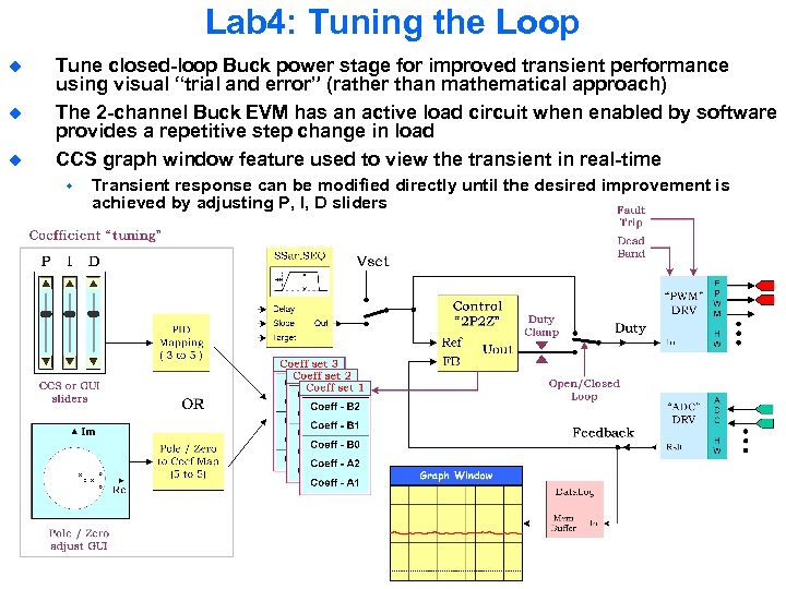 Lab 4: Tuning the Loop u u u Tune closed-loop Buck power stage for improved transient performance using visual “trial and error” (rather than mathematical approach) The 2 -channel Buck EVM has an active load circuit when enabled by software provides a repetitive step change in load CCS graph window feature used to view the transient in real-time Transient response can be modified directly until the desired improvement is achieved by adjusting P, I, D sliders
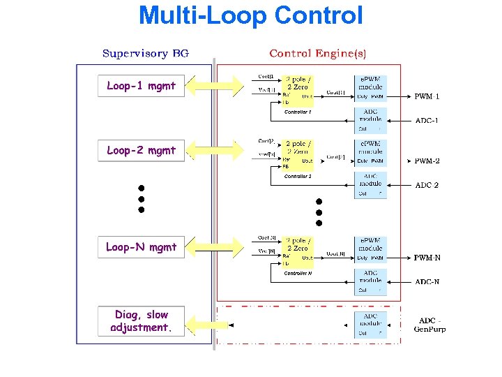 Multi-Loop Control
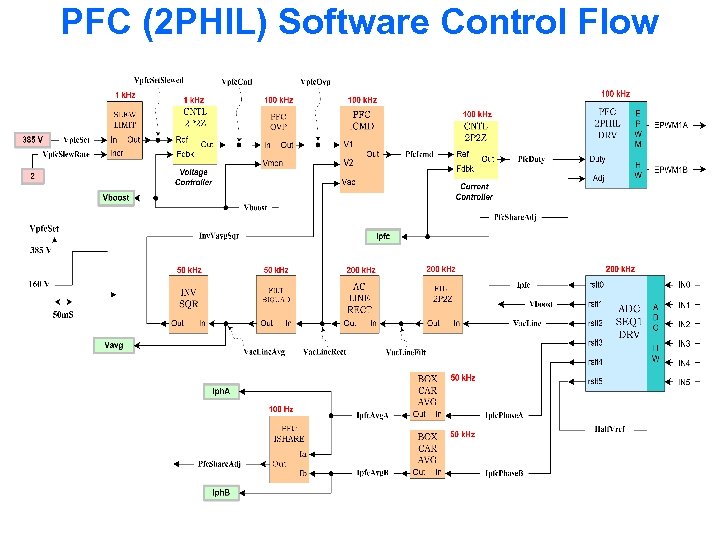 PFC (2 PHIL) Software Control Flow
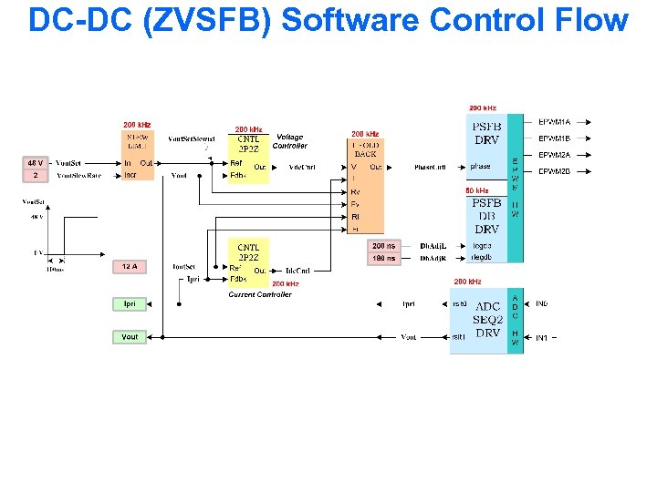 DC-DC (ZVSFB) Software Control Flow
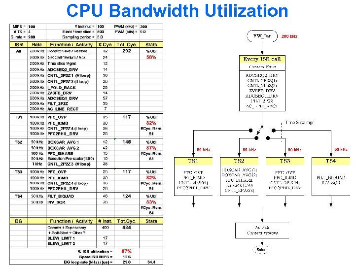 CPU Bandwidth Utilization
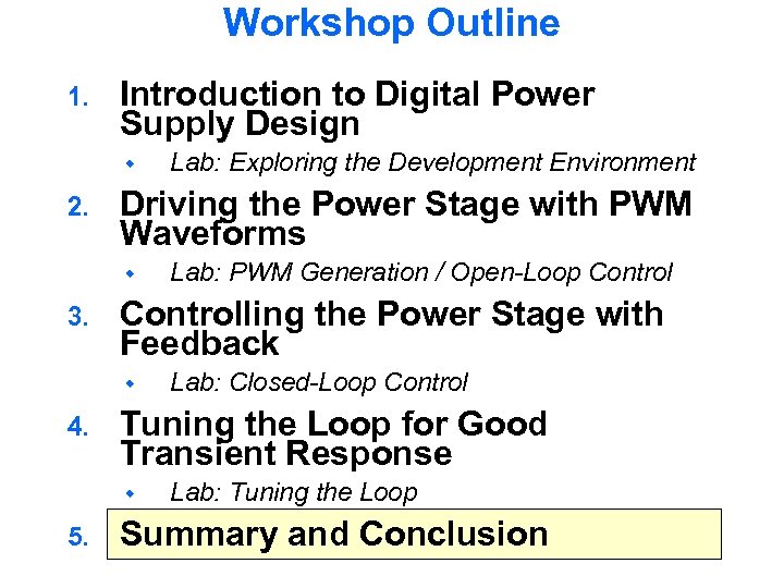 Workshop Outline 1. Introduction to Digital Power Supply Design 2. Driving the Power Stage with PWM Waveforms 3. Lab: Closed-Loop Control Tuning the Loop for Good Transient Response 5. Lab: PWM Generation / Open-Loop Controlling the Power Stage with Feedback 4. Lab: Exploring the Development Environment Lab: Tuning the Loop Summary and Conclusion
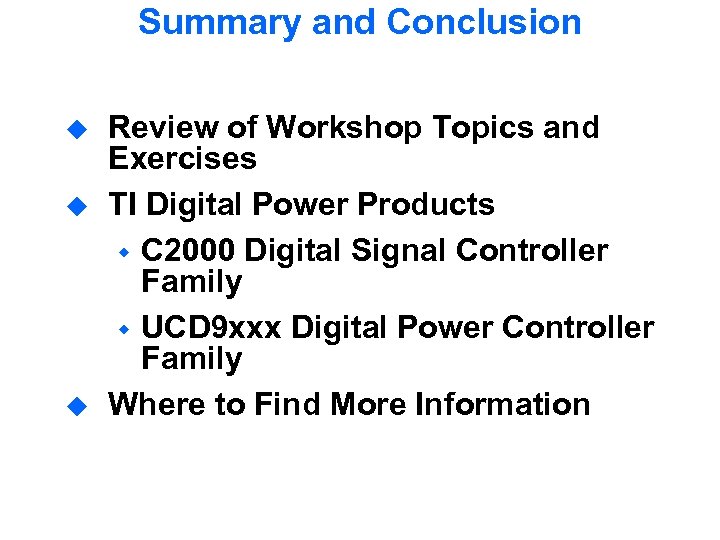 Summary and Conclusion u u u Review of Workshop Topics and Exercises TI Digital Power Products C 2000 Digital Signal Controller Family UCD 9 xxx Digital Power Controller Family Where to Find More Information
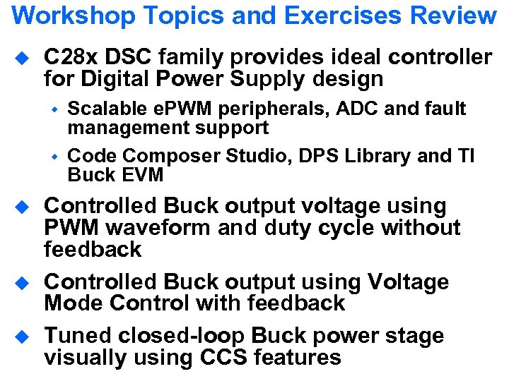 Workshop Topics and Exercises Review u C 28 x DSC family provides ideal controller for Digital Power Supply design u u u Scalable e. PWM peripherals, ADC and fault management support Code Composer Studio, DPS Library and TI Buck EVM Controlled Buck output voltage using PWM waveform and duty cycle without feedback Controlled Buck output using Voltage Mode Control with feedback Tuned closed-loop Buck power stage visually using CCS features
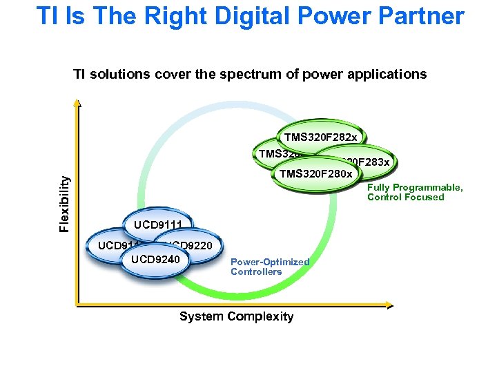 TI Is The Right Digital Power Partner Flexibility TI solutions cover the spectrum of power applications TMS 320 F 282 x TMS 320 F 281 x TMS 320 F 283 x TMS 320 F 280 x Fully Programmable, Control Focused UCD 9111 UCD 9112 UCD 9220 UCD 9240 Power-Optimized Controllers System Complexity
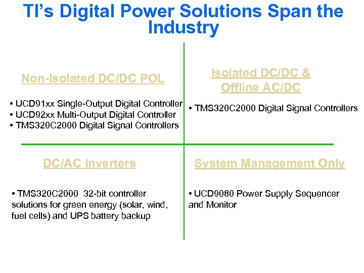 TI’s Digital Power Solutions Span the Industry Non-Isolated DC/DC POL Isolated DC/DC & Offline AC/DC • UCD 91 xx Single-Output Digital Controller • TMS 320 C 2000 Digital Signal Controllers • UCD 92 xx Multi-Output Digital Controller • TMS 320 C 2000 Digital Signal Controllers DC/AC Inverters • TMS 320 C 2000 32 -bit controller solutions for green energy (solar, wind, fuel cells) and UPS battery backup System Management Only • UCD 9080 Power Supply Sequencer and Monitor
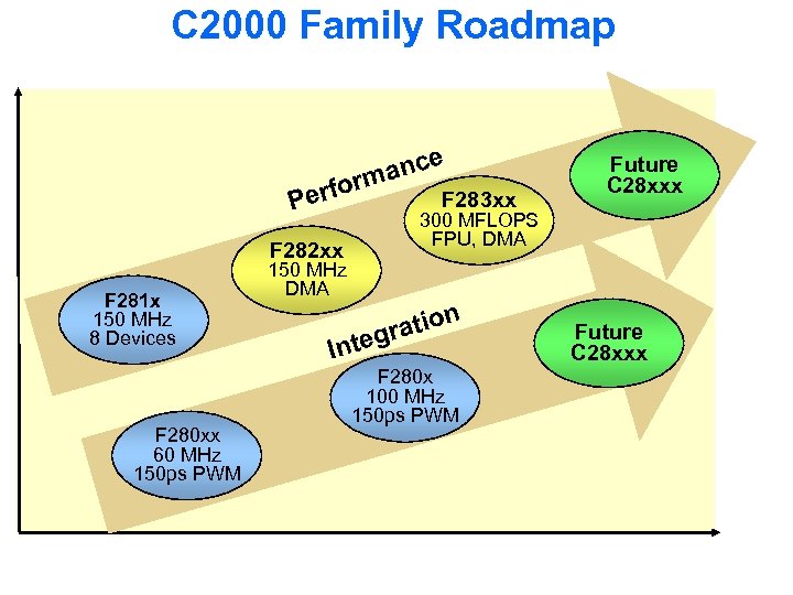 C 2000 Family Roadmap e anc rm o Perf F 283 xx 300 MFLOPS FPU, DMA F 282 xx F 281 x 150 MHz 8 Devices F 280 xx 60 MHz 150 ps PWM Future C 28 xxx 150 MHz DMA n atio egr Int F 280 xx 100 MHz 100 MHz 150 ps PWM Future C 28 xxx
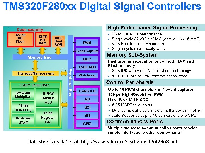 TMS 320 F 280 xx Digital Signal Controllers High Performance Signal Processing Code security 32 -256 KB Flash 12 -36 KB RAM § 8 KB Boot ROM PWM Event Capture Memory Bus C 28 x. TM 32 -bit DSC 32 x 32 -bit Multiplier 32 -bit Timers (3) Real-Time JTAG R M W Atomic ALU Peripheral Bus Interrupt Management QEP 12 -bit ADC Watchdog § § Memory Sub-System Fast program execution out of both RAM and Flash memory § 80 MIPS with Flash Acceleration Technology § 100 MIPS out of RAM for time-critical code Control Peripherals CAN 2. 0 B I 2 C SCI 32 -bit Register File § Up to 100 MHz performance Single cycle 32 x 32 -bit MAC (or dual 16 x 16 MAC) Very Fast Interrupt Response Single cycle read-modify-write SPI GPIO Up to 16 PWM channels and 4 event captures 150 ps High-Resolution PWM Ultra-Fast 12 -bit ADC § 6. 25 MSPS throughput § Dual sample&holds enable simultaneous sampling § Auto Sequencer, up to 16 conversions w/o CPU Communications Ports Multiple standard communication ports provide simple interfaces to other components Datasheet available at: http: //www-s. ti. com/sc/ds/tms 320 f 2808. pdf
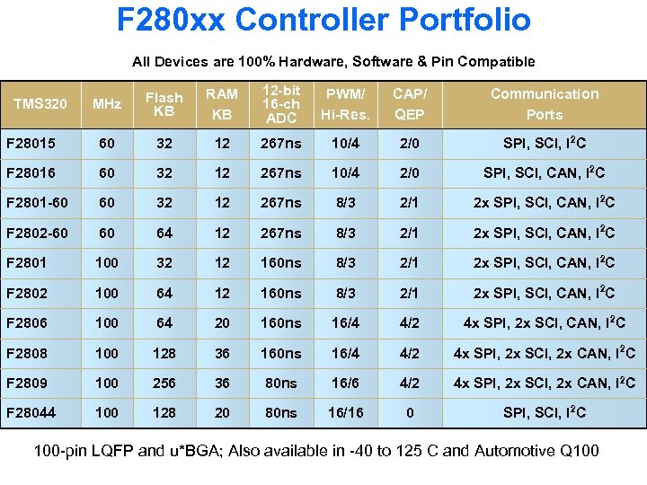 F 280 xx Controller Portfolio All Devices are 100% Hardware, Software & Pin Compatible MHz Flash KB RAM KB 12 -bit 16 -ch ADC PWM/ Hi-Res. CAP/ QEP Communication Ports F 28015 60 32 12 267 ns 10/4 2/0 SPI, SCI, I 2 C F 28016 60 32 12 267 ns 10/4 2/0 SPI, SCI, CAN, I 2 C F 2801 -60 60 32 12 267 ns 8/3 2/1 2 x SPI, SCI, CAN, I 2 C F 2802 -60 60 64 12 267 ns 8/3 2/1 2 x SPI, SCI, CAN, I 2 C F 2801 100 32 12 160 ns 8/3 2/1 2 x SPI, SCI, CAN, I 2 C F 2802 100 64 12 160 ns 8/3 2/1 2 x SPI, SCI, CAN, I 2 C F 2806 100 64 20 160 ns 16/4 4/2 4 x SPI, 2 x SCI, CAN, I 2 C F 2808 100 128 36 160 ns 16/4 4/2 4 x SPI, 2 x SCI, 2 x CAN, I 2 C F 2809 100 256 36 80 ns 16/6 4/2 4 x SPI, 2 x SCI, 2 x CAN, I 2 C F 28044 100 128 20 80 ns 16/16 0 SPI, SCI, I 2 C TMS 320 100 -pin LQFP and u*BGA; Also available in -40 to 125 C and Automotive Q 100
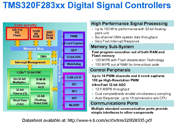 TMS 320 F 283 xx Digital Signal Controllers High Performance Signal Processing Code security 128 -512 KB Flash § 52 -68 KB RAM 8 KB Boot ROM PWM Event Capture Memory Bus Interrupt Management C 28 x. TM 32 -bit DSC 32 x 32 -bit Multiplier 32 -bit Timers (3) Real-Time JTAG R M W Atomic ALU Peripheral Bus DMA QEP 12 -bit ADC Watchdog § Memory Sub-System Fast program execution out of both RAM and Flash memory § 120 MIPS with Flash Acceleration Technology § 150 MIPS out of RAM for time-critical code Control Peripherals CAN 2. 0 B I 2 C SCI 32 -bit Floating. Point Unit § Up to 150 MHz performance with 32 -bit floatingpoint unit Six-channel DMA speeds data throughput Very Fast Interrupt Response SPI Mc. BSP Up to 16 PWM channels and 4 event captures 150 ps High-Resolution PWM Ultra-Fast 12 -bit ADC § 12. 5 MSPS throughput § Dual sample&holds enable simultaneous sampling § Auto Sequencer, up to 16 conversions w/o CPU Communications Ports Multiple standard communication ports provide simple interfaces to other components Datasheet available at: http: //www-s. ti. com/sc/ds/tms 320 f 28335. pdf
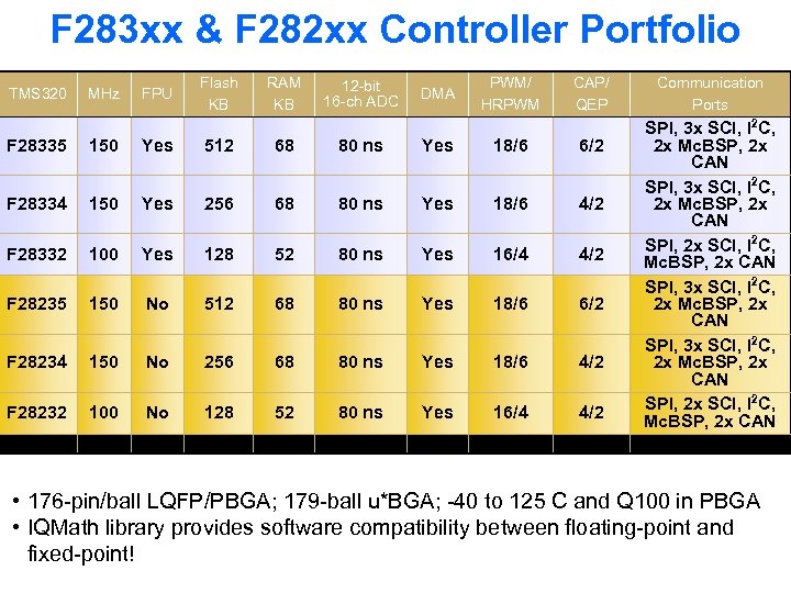 F 283 xx & F 282 xx Controller Portfolio TMS 320 MHz FPU Flash KB RAM KB 12 -bit 16 -ch ADC DMA PWM/ HRPWM CAP/ QEP F 28335 150 Yes 512 68 80 ns Yes 18/6 6/2 F 28334 150 Yes 256 68 80 ns Yes 18/6 4/2 F 28332 100 Yes 128 52 80 ns Yes 16/4 4/2 F 28235 150 No 512 68 80 ns Yes 18/6 6/2 F 28234 150 No 256 68 80 ns Yes 18/6 4/2 F 28232 100 No 128 52 80 ns Yes 16/4 4/2 Communication Ports SPI, 3 x SCI, I 2 C, 2 x Mc. BSP, 2 x CAN SPI, 2 x SCI, I 2 C, Mc. BSP, 2 x CAN • 176 -pin/ball LQFP/PBGA; 179 -ball u*BGA; -40 to 125 C and Q 100 in PBGA • IQMath library provides software compatibility between floating-point and fixed-point!
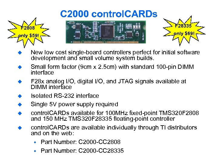 C 2000 control. CARDs F 2808 only $59! u u u u F 28335 only $69! New low cost single-board controllers perfect for initial software development and small volume system builds. Small form factor (9 cm x 2. 5 cm) with standard 100 -pin DIMM interface F 28 x analog I/O, digital I/O, and JTAG signals available at DIMM interface Isolated RS-232 interface Single 5 V power supply required control. CARDs available for 100 MHz fixed-point TMS 320 F 2808 and 150 MHz TMS 320 F 28335 floating-point controller control. CARDs are available individually through TI distributors and on the web: Part Number: C 2000 -CC 2808 Part Number: C 2000 -CC 28335
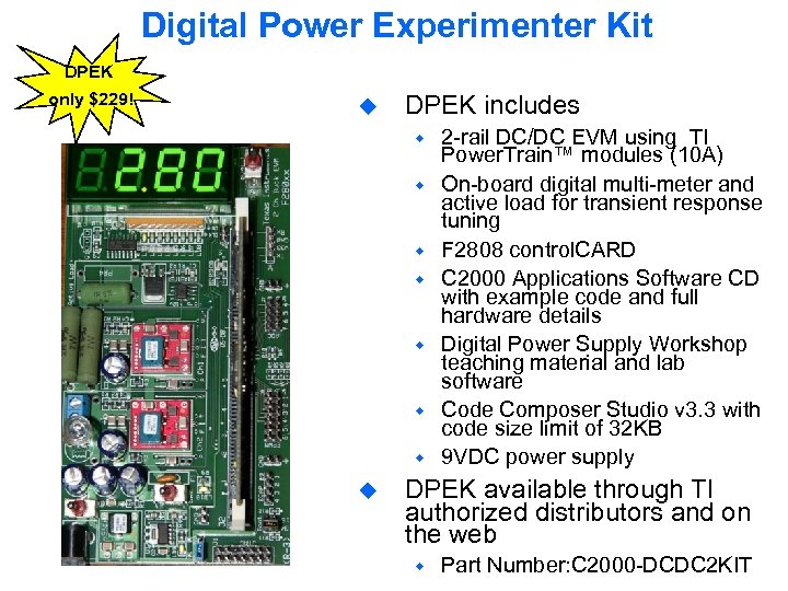 Digital Power Experimenter Kit DPEK only $229! u DPEK includes u 2 -rail DC/DC EVM using TI Power. Train™ modules (10 A) On-board digital multi-meter and active load for transient response tuning F 2808 control. CARD C 2000 Applications Software CD with example code and full hardware details Digital Power Supply Workshop teaching material and lab software Code Composer Studio v 3. 3 with code size limit of 32 KB 9 VDC power supply DPEK available through TI authorized distributors and on the web Part Number: C 2000 -DCDC 2 KIT
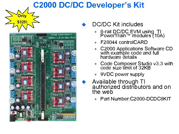 C 2000 DC/DC Developer’s Kit Only $325! u DC/DC Kit includes u 8 -rail DC/DC EVM using TI Power. Train™ modules (10 A) F 28044 control. CARD C 2000 Applications Software CD with example code and full hardware details Code Composer Studio v 3. 3 with code size limit of 32 KB 9 VDC power supply Available through TI authorized distributors and on the web Part Number: C 2000 -DCDC 8 KIT
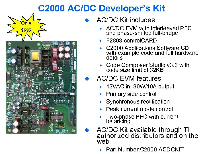 C 2000 AC/DC Developer’s Kit Only u AC/DC Kit includes $695! u AC/DC EVM features u AC/DC EVM with interleaved PFC and phase-shifted full-bridge F 2808 control. CARD C 2000 Applications Software CD with example code and full hardware details Code Composer Studio v 3. 3 with code size limit of 32 KB 12 VAC in, 80 W/10 A output Primary side control Synchronous rectification Peak current mode control Two-phase PFC with current balancing AC/DC Kit available through TI authorized distributors and on the web Part Number: C 2000 -ACDCKIT
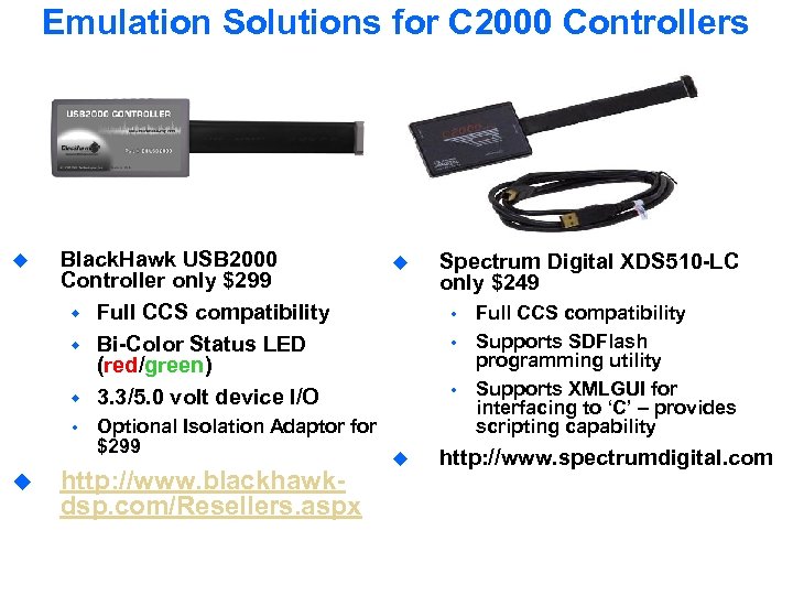 Emulation Solutions for C 2000 Controllers u Black. Hawk USB 2000 Controller only $299 Full CCS compatibility Bi-Color Status LED (red/green) 3. 3/5. 0 volt device I/O u Optional Isolation Adaptor for $299 http: //www. blackhawkdsp. com/Resellers. aspx u Spectrum Digital XDS 510 -LC only $249 u Full CCS compatibility Supports SDFlash programming utility Supports XMLGUI for interfacing to ‘C’ – provides scripting capability http: //www. spectrumdigital. com
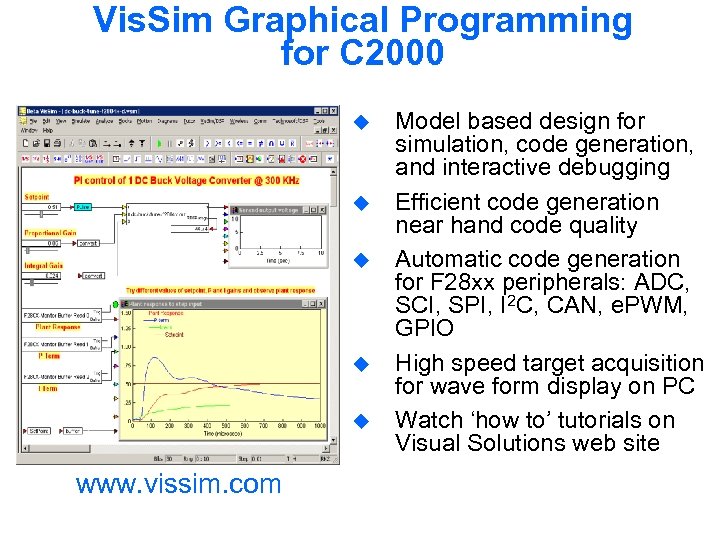 Vis. Sim Graphical Programming for C 2000 u u u www. vissim. com Model based design for simulation, code generation, and interactive debugging Efficient code generation near hand code quality Automatic code generation for F 28 xx peripherals: ADC, SCI, SPI, I 2 C, CAN, e. PWM, GPIO High speed target acquisition for wave form display on PC Watch ‘how to’ tutorials on Visual Solutions web site
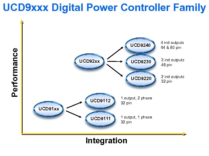 UCD 9 xxx Digital Power Controller Family UCD 9230 UCD 92 xx 4 ind outputs 64 & 80 pin 3 ind outputs 48 pin UCD 9220 Performance UCD 9240 2 ind outputs 32 pin UCD 9112 1 output, 2 phase 32 pin UCD 9111 1 output, 1 phase 32 pin UCD 91 xx Integration
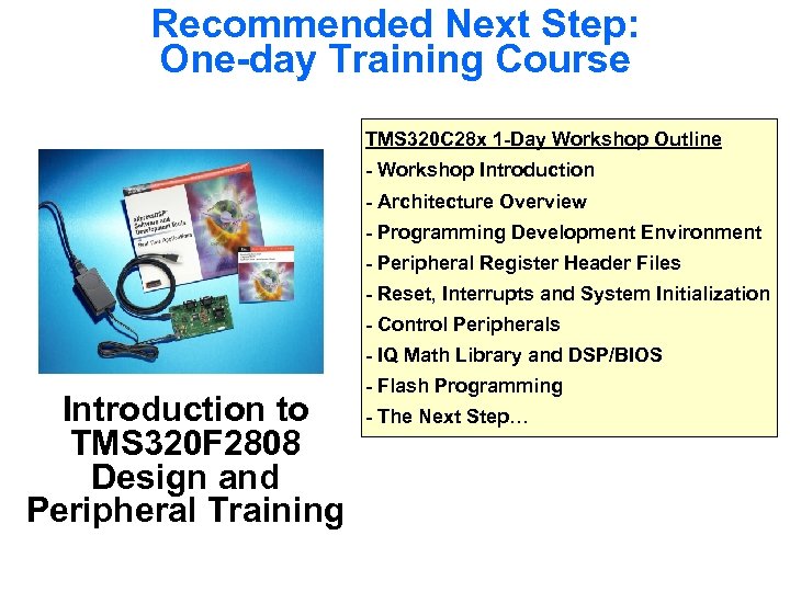 Recommended Next Step: One-day Training Course TMS 320 C 28 x 1 -Day Workshop Outline - Workshop Introduction - Architecture Overview - Programming Development Environment - Peripheral Register Header Files - Reset, Interrupts and System Initialization - Control Peripherals - IQ Math Library and DSP/BIOS Introduction to TMS 320 F 2808 Design and Peripheral Training - Flash Programming - The Next Step…
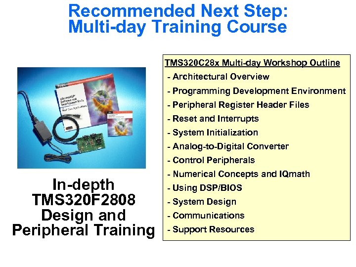 Recommended Next Step: Multi-day Training Course TMS 320 C 28 x Multi-day Workshop Outline - Architectural Overview - Programming Development Environment - Peripheral Register Header Files - Reset and Interrupts - System Initialization - Analog-to-Digital Converter - Control Peripherals In-depth TMS 320 F 2808 Design and Peripheral Training - Numerical Concepts and IQmath - Using DSP/BIOS - System Design - Communications - Support Resources
 For More Information. . . Internet Website: http: //www. ti. com FAQ: http: //www-k. ext. ti. com/sc/technical_support/knowledgebase. htm Device information my. ti. com Application notes News and events Technical documentation Training Enroll in Technical Training: http: //www. ti. com/sc/training USA - Product Information Center ( PIC ) Phone: 800 -477 -8924 or 972 -644 -5580 Email: support@ti. com Information and support for all TI Semiconductor products/tools Submit suggestions and errata for tools, silicon and documents
 European Product Information Center (EPIC) Web: http: //www-k. ext. ti. com/sc/technical_support/pic/euro. htm Phone: Language Belgium (English) France Germany Israel (English) Italy Netherlands (English) Spain Sweden (English) United Kingdom Finland (English) Fax: All Languages Number +32 (0) 27 45 55 32 +33 (0) 1 30 70 11 64 +49 (0) 8161 80 33 11 1800 949 0107 (free phone) 800 79 11 37 (free phone) +31 (0) 546 87 95 45 +34 902 35 40 28 +46 (0) 8587 555 22 +44 (0) 1604 66 33 99 +358(0) 9 25 17 39 48 +49 (0) 8161 80 2045 Email: epic@ti. com Literature, Sample Requests and Analog EVM Ordering Information, Technical and Design support for all Catalog TI Semiconductor products/tools Submit suggestions and errata for tools, silicon and documents
 Technical Training Organization ti


