7d1218c5aee8ba78723232769abc91ef.ppt
- Количество слайдов: 157
Block Owner: Brain Felsmenn
Capstone Design Team #2 Team Members • • • Eenas Omari Ayodeji Opadeyi Kevin Erickson Brian Felsmann Rick Ryer • • • BSEE, BSCS BSEE 2
Millennium Infrared Sound System • Project Description: – A wireless audio system using infrared technology – Primarily designed for Home Theater Systems to eliminate speaker wires – Accepts any analog audio input and transmits the signal to the wireless amplifiers. Uses owner’s already existing speakers. – Not proprietary to any audio manufactures equipment 3
Millennium Infrared Sound System • Benefits of Product: – A plug-n-play system compatible with existing audio receiver and speakers – Eliminates speaker wires around the living room – Does not use RF technology which could have inference from other popular home electronic devices (telephones, Wi-Fi, Radio) – Fast easy installation 4

Millennium Infrared Sound System • Targeted Market of Product: – Consumer Electronics market – Marketed in the United States and Canada • Targeted Demographic – 18 – 30 year olds with Home Theater Systems • MSRP – $100 -- $125 5
Millennium Infrared Sound System • Project Selection: – Reasonable low cost project – Unique product – Similar, more expensive, products using RF technology – An interest from team members 6
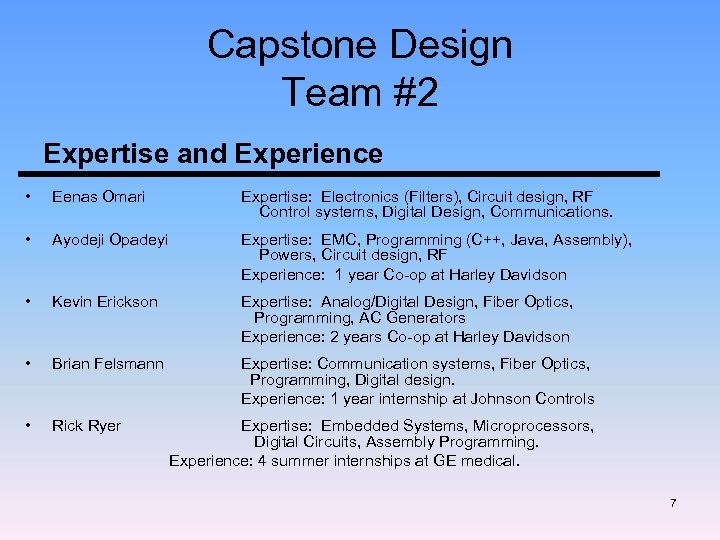
Capstone Design Team #2 Expertise and Experience • Eenas Omari • Ayodeji Opadeyi Expertise: EMC, Programming (C++, Java, Assembly), Powers, Circuit design, RF Experience: 1 year Co-op at Harley Davidson • Kevin Erickson Expertise: Analog/Digital Design, Fiber Optics, Programming, AC Generators Experience: 2 years Co-op at Harley Davidson • Brian Felsmann Expertise: Communication systems, Fiber Optics, Programming, Digital design. Experience: 1 year internship at Johnson Controls • Rick Ryer Expertise: Electronics (Filters), Circuit design, RF Control systems, Digital Design, Communications. Expertise: Embedded Systems, Microprocessors, Digital Circuits, Assembly Programming. Experience: 4 summer internships at GE medical. 7

Capstone Design Team #2 • Available Resources: – 1200 – 1600 Man-hours • 15 -20 hours/week per team member • Includes lab time, periodic meetings, and personal time – $500 -$750 for material and prototyping • $100 -$125 per team member • Actual Resources: – 1000 Man-hours – $250 for materials and prototyping 8
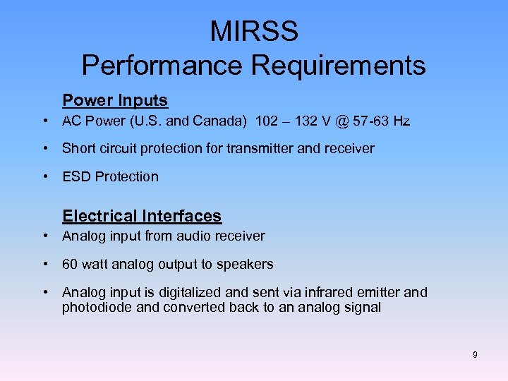
MIRSS Performance Requirements Power Inputs • AC Power (U. S. and Canada) 102 – 132 V @ 57 -63 Hz • Short circuit protection for transmitter and receiver • ESD Protection Electrical Interfaces • Analog input from audio receiver • 60 watt analog output to speakers • Analog input is digitalized and sent via infrared emitter and photodiode and converted back to an analog signal 9
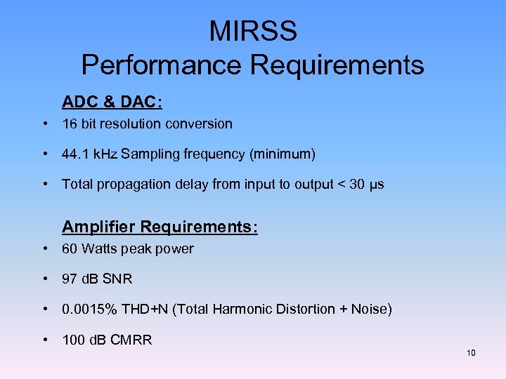
MIRSS Performance Requirements ADC & DAC: • 16 bit resolution conversion • 44. 1 k. Hz Sampling frequency (minimum) • Total propagation delay from input to output < 30 μs Amplifier Requirements: • 60 Watts peak power • 97 d. B SNR • 0. 0015% THD+N (Total Harmonic Distortion + Noise) • 100 d. B CMRR 10
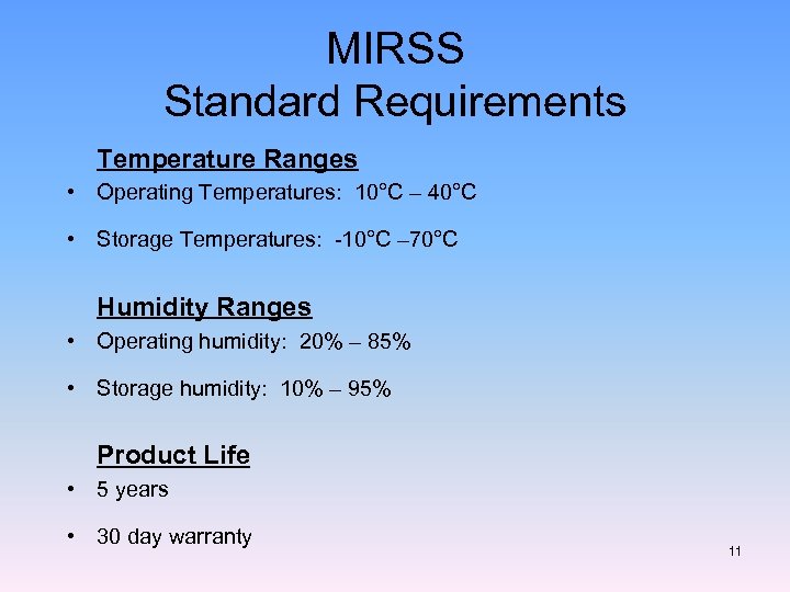
MIRSS Standard Requirements Temperature Ranges • Operating Temperatures: 10°C – 40°C • Storage Temperatures: -10°C – 70°C Humidity Ranges • Operating humidity: 20% – 85% • Storage humidity: 10% – 95% Product Life • 5 years • 30 day warranty 11
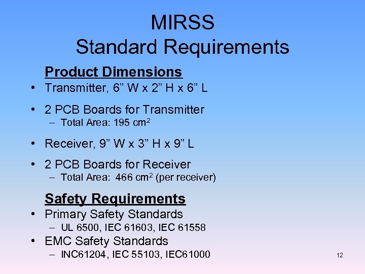
MIRSS Standard Requirements Product Dimensions • Transmitter, 6” W x 2” H x 6” L • 2 PCB Boards for Transmitter – Total Area: 195 cm 2 • Receiver, 9” W x 3” H x 9” L • 2 PCB Boards for Receiver – Total Area: 466 cm 2 (per receiver) Safety Requirements • Primary Safety Standards – UL 6500, IEC 61603, IEC 61558 • EMC Safety Standards – INC 61204, IEC 55103, IEC 61000 12
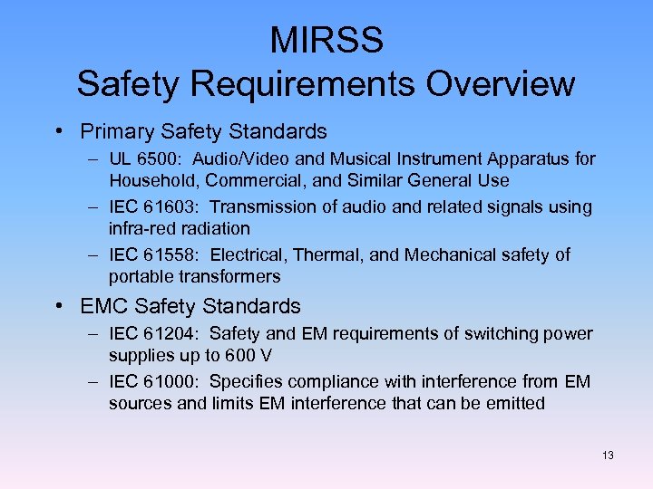
MIRSS Safety Requirements Overview • Primary Safety Standards – UL 6500: Audio/Video and Musical Instrument Apparatus for Household, Commercial, and Similar General Use – IEC 61603: Transmission of audio and related signals using infra-red radiation – IEC 61558: Electrical, Thermal, and Mechanical safety of portable transformers • EMC Safety Standards – IEC 61204: Safety and EM requirements of switching power supplies up to 600 V – IEC 61000: Specifies compliance with interference from EM sources and limits EM interference that can be emitted 13
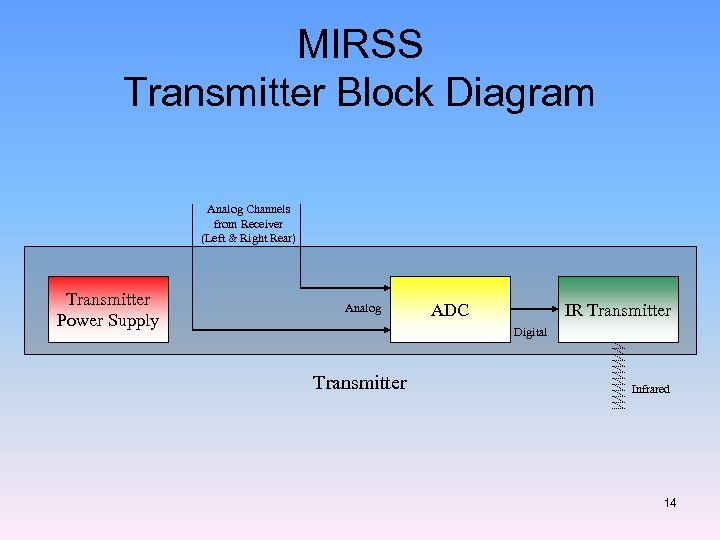
MIRSS Transmitter Block Diagram Analog Channels from Receiver (Left & Right Rear) Transmitter Power Supply Analog ADC IR Transmitter Digital Transmitter Infrared 14
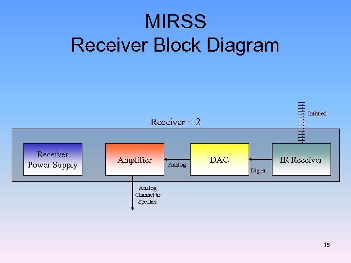
MIRSS Receiver Block Diagram Infrared Receiver × 2 Receiver Power Supply Amplifier Analog DAC IR Receiver Digital Analog Channel to Speaker 15
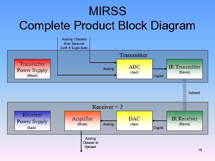
MIRSS Complete Product Block Diagram Analog Channels from Receiver (Left & Right Rear) Transmitter Power Supply Analog (Eenas) ADC (Ayo) IR Transmitter Digital (Kevin) Infrared Receiver × 2 Receiver Power Supply (Rick) Amplifier (Brian) Analog Channel to Speaker DAC Analog (Ayo) IR Receiver Digital (Kevin) 16
MIRSS Block Allocations 17
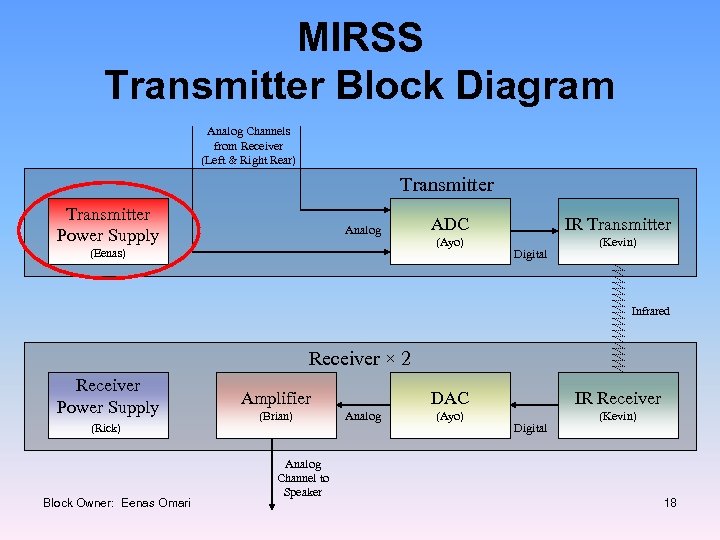
MIRSS Transmitter Block Diagram Analog Channels from Receiver (Left & Right Rear) Transmitter Power Supply Analog (Eenas) ADC (Ayo) IR Transmitter Digital (Kevin) Infrared Receiver × 2 Receiver Power Supply (Rick) Block Owner: Eenas Omari Amplifier (Brian) Analog Channel to Speaker DAC Analog (Ayo) IR Receiver Digital (Kevin) 18
Transmitter Power Supply • Block Description – An electrical device that transforms the standard wall outlet electricity (AC) into lower voltages (DC) – Will supply voltage to both the Analog to Digital converter (ADC) and the Infrared transmitter (IR Transmitter). Block Owner: Eenas Omari 19
Transmitter Power Supply Standard Requirements Temperature: - Operating Temperature: 10 – 60 o. C. - Storage Temperature: 10 – 40 o. C. Humidity: - Operating Humidity: 20– 85 %Rh. - Storage Humidity: 10 – 95 %Rh Block Owner: Eenas Omari 20
Transmitter Power Supply Standard Requirements • Mechanical: - Max PCB Area: 103. 23 cm 2 - Max Volume: 524. 41 cm 3. - Max Mass: 0. 907 kg - # PCB: 1. - # Connectors : 1 • Power: Voltage Range (AC): 102 V < Vin < 132 V • Life Cycle: - Life : 5 years - Reliability : 5 years. - Disposal : Recycle. Block Owner: Eenas Omari 21
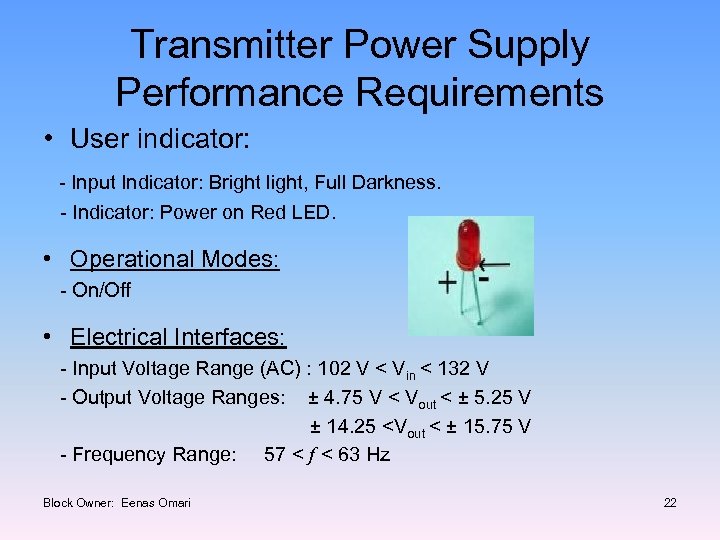
Transmitter Power Supply Performance Requirements • User indicator: - Input Indicator: Bright light, Full Darkness. - Indicator: Power on Red LED. • Operational Modes: - On/Off • Electrical Interfaces: - Input Voltage Range (AC) : 102 V < Vin < 132 V - Output Voltage Ranges: ± 4. 75 V < Vout < ± 5. 25 V ± 14. 25 <Vout < ± 15. 75 V - Frequency Range: 57 < f < 63 Hz Block Owner: Eenas Omari 22
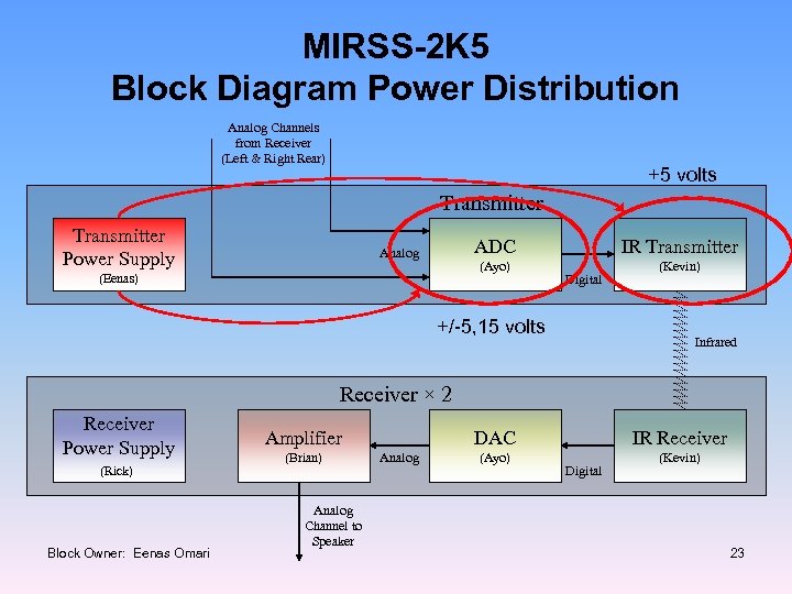
MIRSS-2 K 5 Block Diagram Power Distribution Analog Channels from Receiver (Left & Right Rear) +5 volts Transmitter Power Supply ADC Analog (Ayo) (Eenas) IR Transmitter Digital +/-5, 15 volts (Kevin) Infrared Receiver × 2 Receiver Power Supply (Rick) Block Owner: Eenas Omari Amplifier (Brian) Analog Channel to Speaker DAC Analog (Ayo) IR Receiver Digital (Kevin) 23
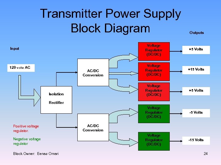
Transmitter Power Supply Block Diagram Outputs Voltage Regulator (DC/DC) AC/DC Conversion Isolation Voltage Regulator (DC/DC) +15 Volts +5 Volts Voltage Regulator (DC/DC) 120 volts AC +5 Volts Voltage Regulator (DC/DC) Input -5 Volts Voltage Regulator (DC/DC) -15 Volts Rectifier Positive voltage regulator. Negative voltage regulator Block Owner: Eenas Omari AC/DC Conversion 24
Block Owner: Eenas Omari 25
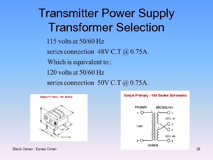
Transmitter Power Supply Transformer Selection Block Owner: Eenas Omari 26
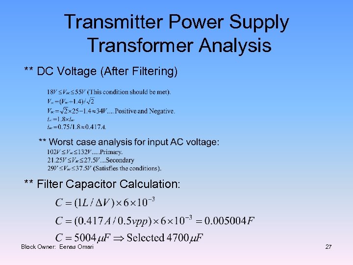
Transmitter Power Supply Transformer Analysis ** DC Voltage (After Filtering) ** Filter Capacitor Calculation: Block Owner: Eenas Omari 27
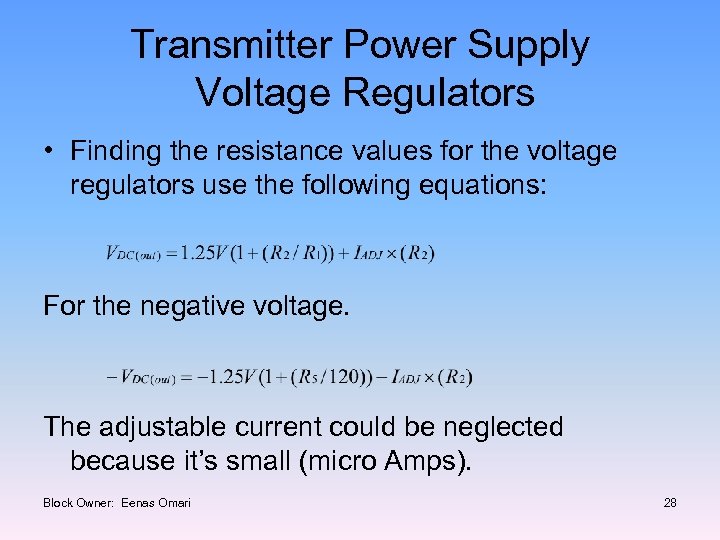
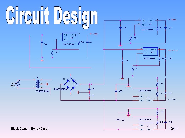
Transmitter Power Supply Voltage Regulators • Finding the resistance values for the voltage regulators use the following equations: For the negative voltage. The adjustable current could be neglected because it’s small (micro Amps). Block Owner: Eenas Omari 28
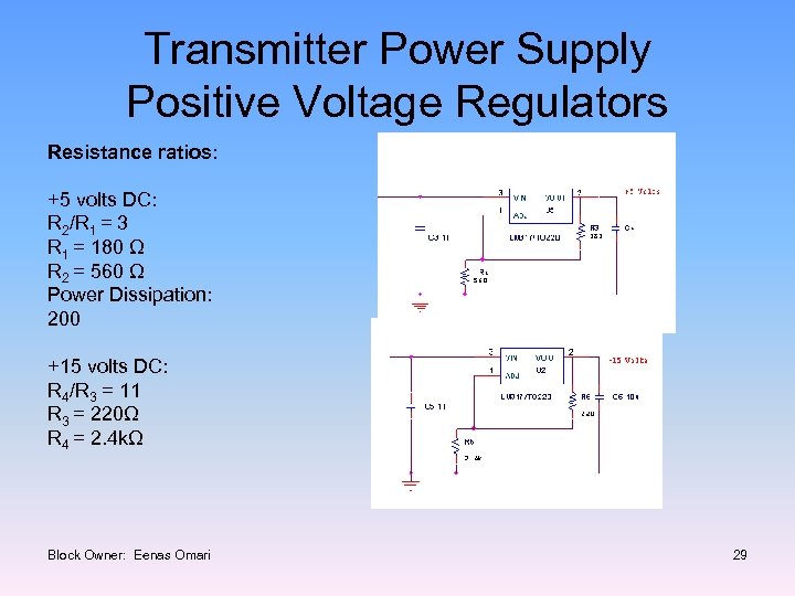
Transmitter Power Supply Positive Voltage Regulators Resistance ratios: +5 volts DC: R 2/R 1 = 3 R 1 = 180 Ω R 2 = 560 Ω Power Dissipation: 200 +15 volts DC: R 4/R 3 = 11 R 3 = 220Ω R 4 = 2. 4 kΩ Block Owner: Eenas Omari 29
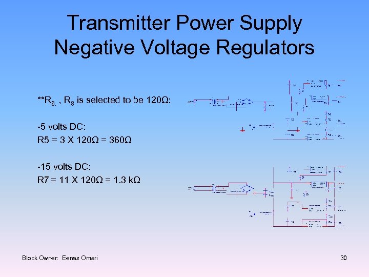
Transmitter Power Supply Negative Voltage Regulators **R 6, , R 8 is selected to be 120Ω: -5 volts DC: R 5 = 3 X 120Ω = 360Ω -15 volts DC: R 7 = 11 X 120Ω = 1. 3 kΩ Block Owner: Eenas Omari 30
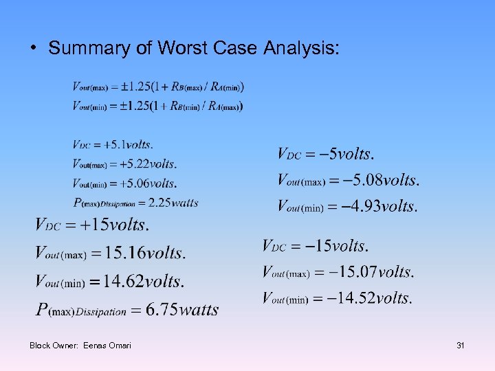
• Summary of Worst Case Analysis: Block Owner: Eenas Omari 31
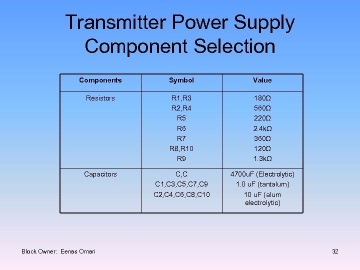
Transmitter Power Supply Component Selection Components Symbol Value Resistors R 1, R 3 R 2, R 4 R 5 R 6 R 7 R 8, R 10 R 9 180Ω 560Ω 220Ω 2. 4 kΩ 360Ω 120Ω 1. 3 kΩ Capacitors C, C C 1, C 3, C 5, C 7, C 9 C 2, C 4, C 6, C 8, C 10 4700 u. F (Electrolytic) 1. 0 u. F (tantalum) 10 u. F (alum electrolytic) Block Owner: Eenas Omari 32
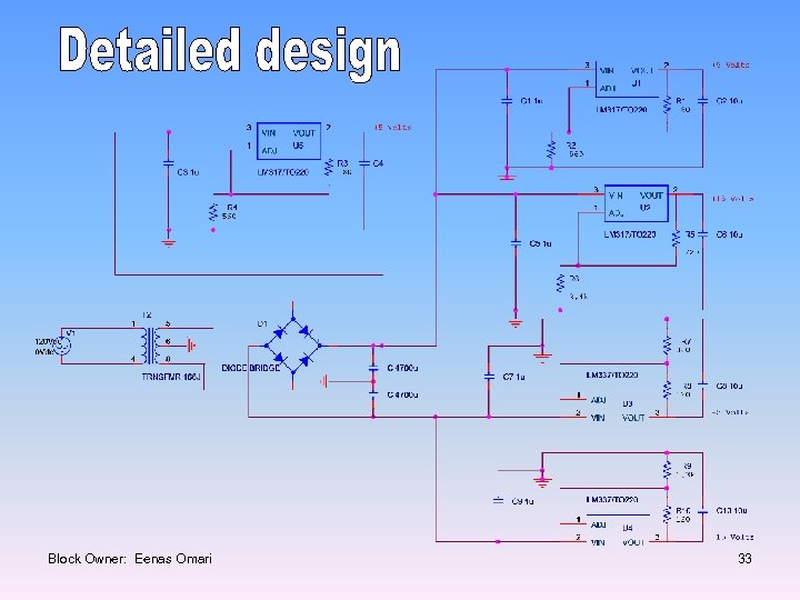
Block Owner: Eenas Omari 33
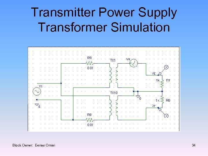
Transmitter Power Supply Transformer Simulation Block Owner: Eenas Omari 34
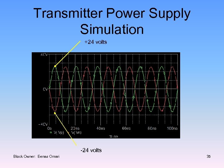
Transmitter Power Supply Simulation +24 volts -24 volts Block Owner: Eenas Omari 35
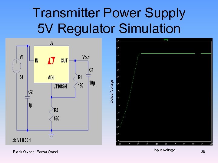
Output Voltage Transmitter Power Supply 5 V Regulator Simulation Block Owner: Eenas Omari Input Voltage 36
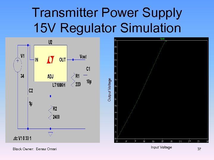
Output Voltage Transmitter Power Supply 15 V Regulator Simulation Block Owner: Eenas Omari Input Voltage 37
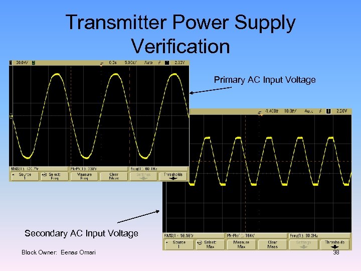
Transmitter Power Supply Verification Primary AC Input Voltage Secondary AC Input Voltage Block Owner: Eenas Omari 38
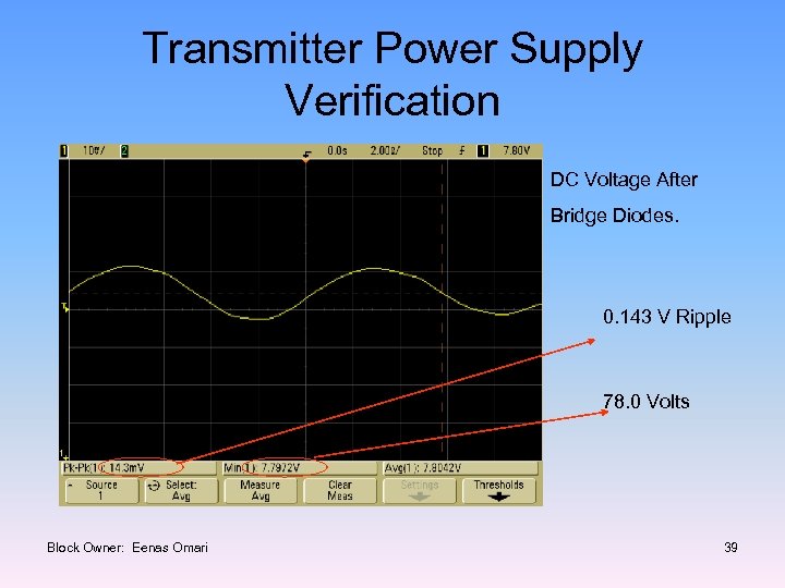
Transmitter Power Supply Verification DC Voltage After Bridge Diodes. 0. 143 V Ripple 78. 0 Volts Block Owner: Eenas Omari 39
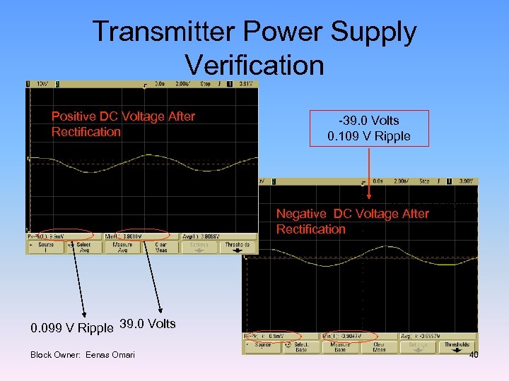
Transmitter Power Supply Verification Positive DC Voltage After Rectification -39. 0 Volts 0. 109 V Ripple 0. 143 V Ripple Negative DC Voltage After Rectification 0. 099 V Ripple 39. 0 Volts Block Owner: Eenas Omari 40
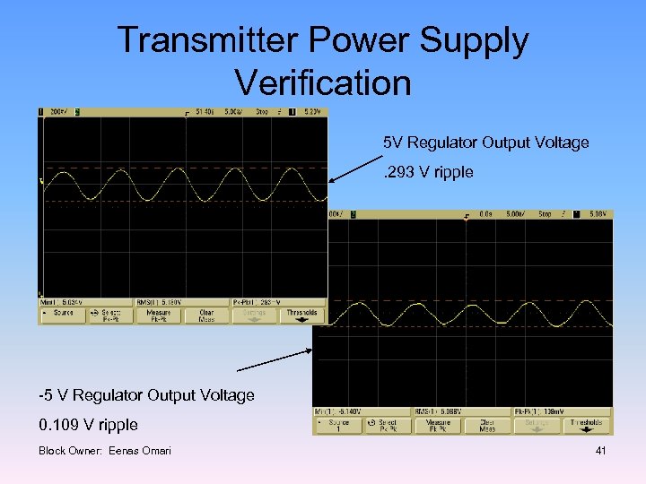
Transmitter Power Supply Verification 5 V Regulator Output Voltage. 293 V ripple -5 V Regulator Output Voltage 0. 109 V ripple Block Owner: Eenas Omari 41
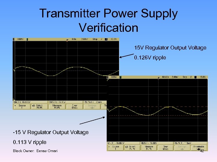
Transmitter Power Supply Verification 15 V Regulator Output Voltage 0. 126 V ripple -15 V Regulator Output Voltage 0. 113 V ripple Block Owner: Eenas Omari 42
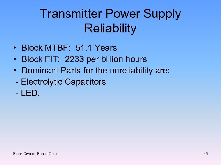
Transmitter Power Supply Reliability • Block MTBF: 51. 1 Years • Block FIT: 2233 per billion hours • Dominant Parts for the unreliability are: - Electrolytic Capacitors - LED. Block Owner: Eenas Omari 43
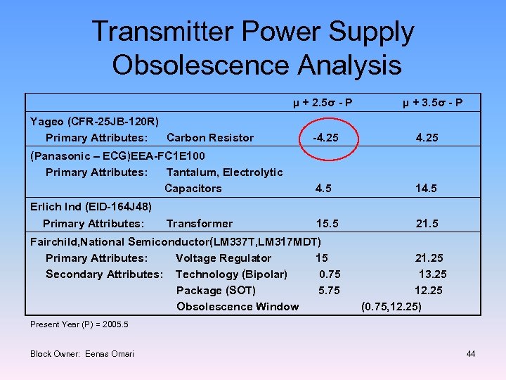
Transmitter Power Supply Obsolescence Analysis µ + 2. 5σ - P µ + 3. 5σ - P Yageo (CFR-25 JB-120 R) Primary Attributes: Carbon Resistor -4. 25 (Panasonic – ECG)EEA-FC 1 E 100 Primary Attributes: Tantalum, Electrolytic Capacitors 4. 5 14. 5 Erlich Ind (EID-164 J 48) Primary Attributes: 15. 5 21. 5 Transformer Fairchild, National Semiconductor(LM 337 T, LM 317 MDT) Primary Attributes: Voltage Regulator 15 Secondary Attributes: Technology (Bipolar) 0. 75 Package (SOT) 5. 75 Obsolescence Window 21. 25 13. 25 12. 25 (0. 75, 12. 25) Present Year (P) = 2005. 5 Block Owner: Eenas Omari 44
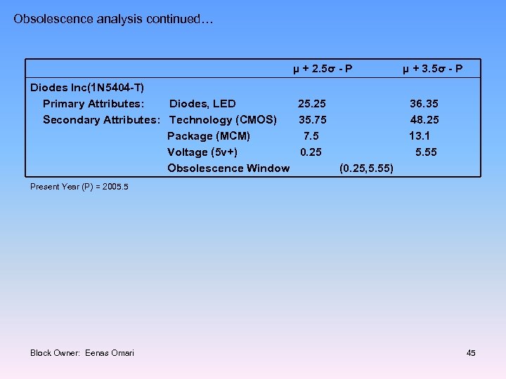
Obsolescence analysis continued… µ + 2. 5σ - P Diodes Inc(1 N 5404 -T) Primary Attributes: Diodes, LED 25. 25 Secondary Attributes: Technology (CMOS) 35. 75 Package (MCM) 7. 5 Voltage (5 v+) 0. 25 Obsolescence Window µ + 3. 5σ - P 36. 35 48. 25 13. 1 5. 55 (0. 25, 5. 55) Present Year (P) = 2005. 5 Block Owner: Eenas Omari 45
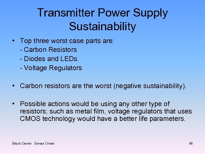
Transmitter Power Supply Sustainability • Top three worst case parts are: - Carbon Resistors - Diodes and LEDs. - Voltage Regulators • Carbon resistors are the worst (negative sustainability). • Possible actions would be using any other type of resistors; such as metal film, voltage regulators that uses CMOS technology would have a better life parameters. Block Owner: Eenas Omari 46
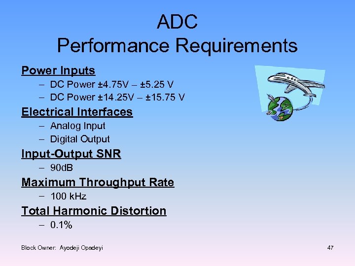
ADC Performance Requirements Power Inputs – DC Power ± 4. 75 V – ± 5. 25 V – DC Power ± 14. 25 V – ± 15. 75 V Electrical Interfaces – Analog Input – Digital Output Input-Output SNR – 90 d. B Maximum Throughput Rate − 100 k. Hz Total Harmonic Distortion – 0. 1% Block Owner: Ayodeji Opadeyi 47
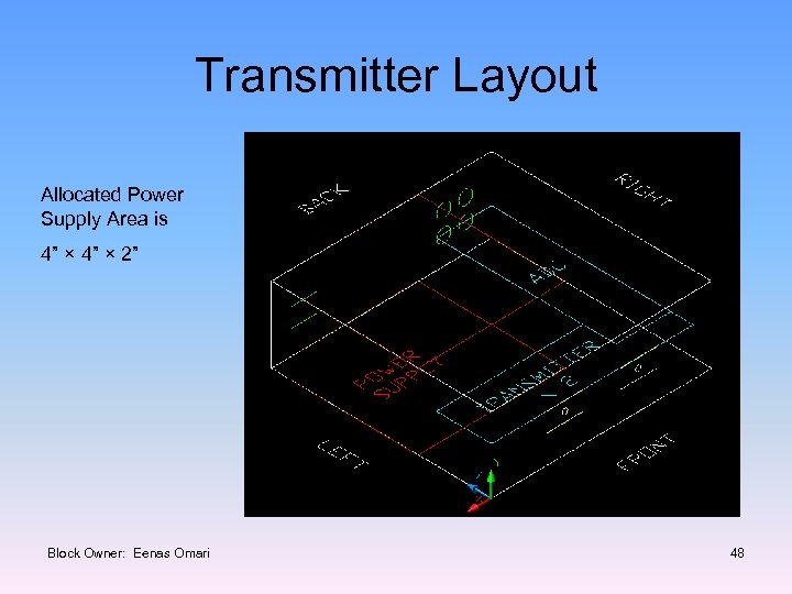
Transmitter Layout Allocated Power Supply Area is 4” × 2” Block Owner: Eenas Omari 48
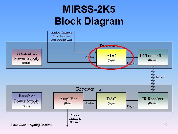
MIRSS-2 K 5 Block Diagram Analog Channels from Receiver (Left & Right Rear) Transmitter Power Supply Analog (Eenas) ADC (Ayo) IR Transmitter Digital (Kevin) Infrared Receiver × 2 Receiver Power Supply (Rick) Block Owner: Ayodeji Opadeyi Amplifier (Brian) Analog Channel to Speaker DAC Analog (Ayo) IR Receiver Digital (Kevin) 49
ADC Standard Requirements Temperature Ranges – Operating Temperatures -40°C – 85°C – Storage Temperatures -65°C – 150°C Max Volume – 103. 24 cm 3 Max Mass – 0. 1 kg Block Owner: Ayodeji Opadeyi 50
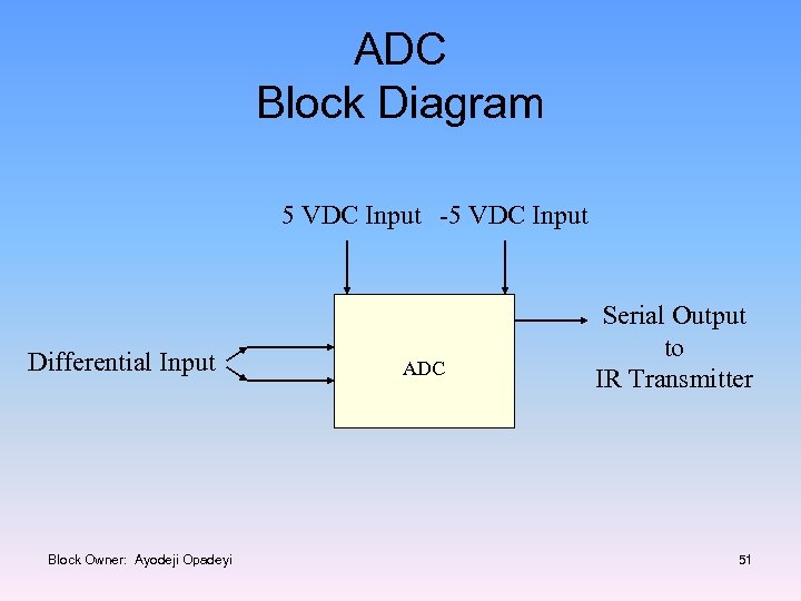
ADC Block Diagram 5 VDC Input -5 VDC Input Differential Input Block Owner: Ayodeji Opadeyi ADC Serial Output to IR Transmitter 51
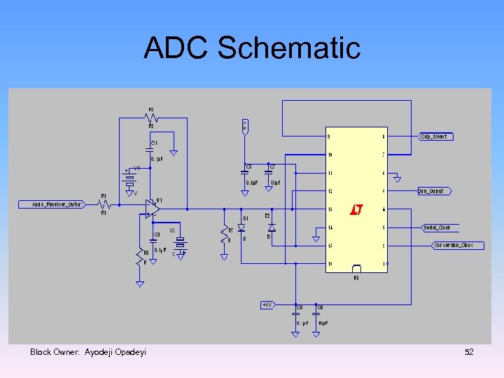
ADC Schematic Block Owner: Ayodeji Opadeyi 52
ADC Key Components Product – Eight 5% tolerance resistors, ½ W • – Two op-amps • – Part of the signal conditioning to reduce the analog input to the ADC High speed, low noise to condition the input signal by attenuating the analog input 2 Max 195 chips (Surface mount) • • • 85 k. Sps max 16 bit resolution, serial output 1. 7 MHz max clock frequency Block Owner: Ayodeji Opadeyi 53
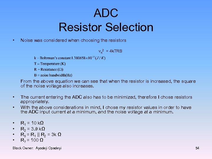
ADC Resistor Selection • Noise was considered when choosing the resistors vn 2 = 4 k. TRB From the above equation we can see that when the resistor is increased, the square of the noise voltage also increases. • • • The current entering the ADC also has to be minimized, therefore I chose resistors appropriately. With the above considerations in mind, I chose my resistor values in order to have the ADC input current at a minimum, and the noise voltage at a minimum. R 1 = 10 kΩ R 2 = 3. 9 kΩ R 5 = R 1 || R 2 = 3 k Ω R 7 = 100 Ω Block Owner: Ayodeji Opadeyi 54
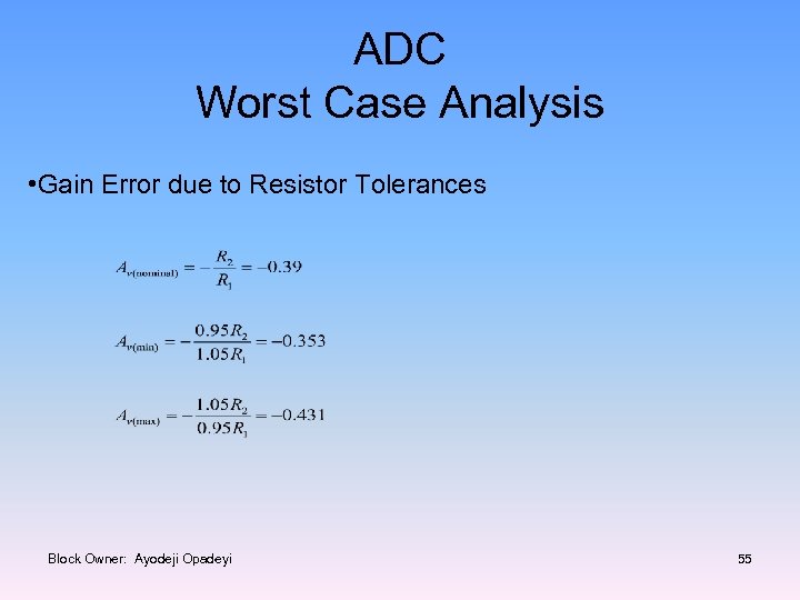
ADC Worst Case Analysis • Gain Error due to Resistor Tolerances Block Owner: Ayodeji Opadeyi 55
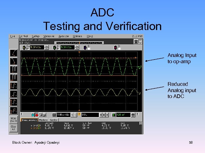
ADC Testing and Verification Analog Input to op-amp Reduced Analog input to ADC Block Owner: Ayodeji Opadeyi 56
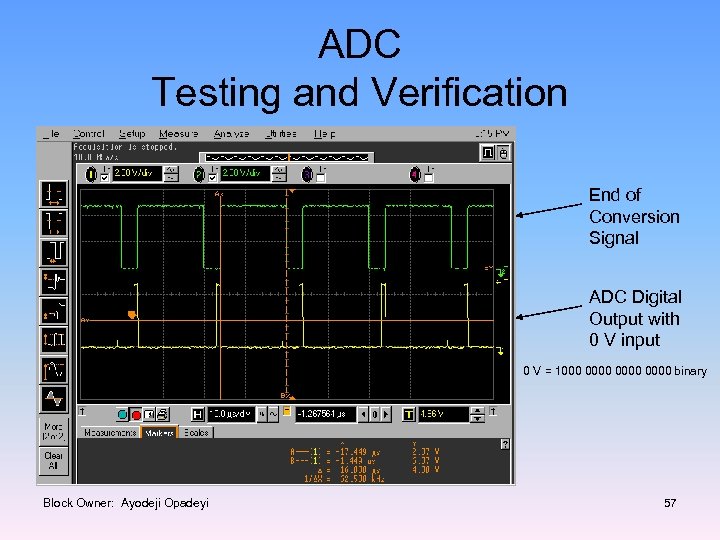
ADC Testing and Verification End of Conversion Signal ADC Digital Output with 0 V input 0 V = 1000 0000 binary Block Owner: Ayodeji Opadeyi 57
ADC Reliability Analysis • Block FITs: – 745. 1 failure Units per billion hours • MTBF: – 153. 1 years • Most unreliable – ADC, and Capacitors • Possible solutions to improve the reliability – Use more reliable capacitors – ADC cannot be changed Block Owner: Ayodeji Opadeyi 58
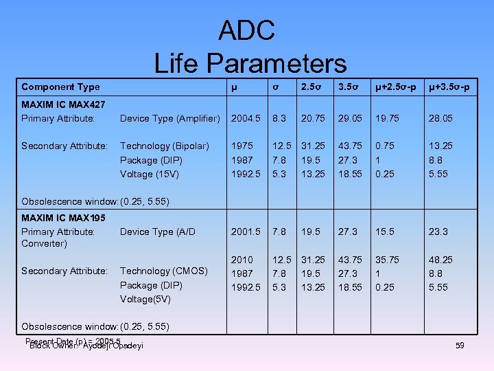
ADC Life Parameters Component Type μ σ 2. 5σ 3. 5σ μ+2. 5σ-p μ+3. 5σ-p MAXIM IC MAX 427 Primary Attribute: 2004. 5 8. 3 20. 75 29. 05 19. 75 28. 05 1975 1987 1992. 5 12. 5 7. 8 5. 3 31. 25 19. 5 13. 25 43. 75 27. 3 18. 55 0. 75 1 0. 25 13. 25 8. 8 5. 55 2001. 5 7. 8 19. 5 27. 3 15. 5 23. 3 2010 1987 1992. 5 12. 5 7. 8 5. 3 31. 25 19. 5 13. 25 43. 75 27. 3 18. 55 35. 75 1 0. 25 48. 25 8. 8 5. 55 Device Type (Amplifier) Secondary Attribute: Technology (Bipolar) Package (DIP) Voltage (15 V) Obsolescence window: (0. 25, 5. 55) MAXIM IC MAX 195 Primary Attribute: Converter) Device Type (A/D Secondary Attribute: Technology (CMOS) Package (DIP) Voltage(5 V) Obsolescence window: (0. 25, 5. 55) Present Date (p) = 2005. 5 Block Owner: Ayodeji Opadeyi 59
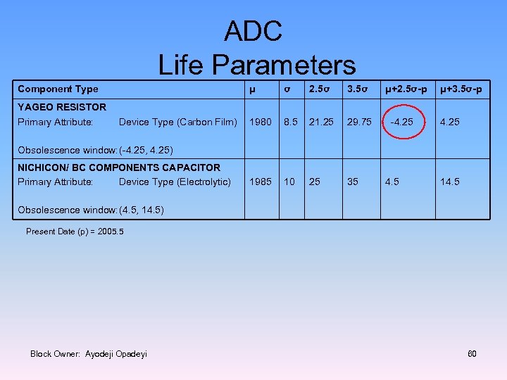
ADC Life Parameters Component Type YAGEO RESISTOR Primary Attribute: μ Device Type (Carbon Film) σ 2. 5σ 3. 5σ μ+2. 5σ-p μ+3. 5σ-p 1980 8. 5 21. 25 29. 75 -4. 25 1985 10 25 35 4. 5 14. 5 Obsolescence window: (-4. 25, 4. 25) NICHICON/ BC COMPONENTS CAPACITOR Primary Attribute: Device Type (Electrolytic) Obsolescence window: (4. 5, 14. 5) Present Date (p) = 2005. 5 Block Owner: Ayodeji Opadeyi 60
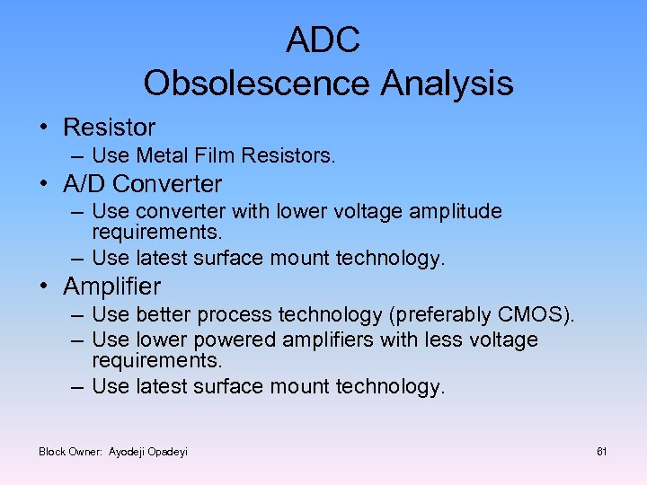
ADC Obsolescence Analysis • Resistor – Use Metal Film Resistors. • A/D Converter – Use converter with lower voltage amplitude requirements. – Use latest surface mount technology. • Amplifier – Use better process technology (preferably CMOS). – Use lower powered amplifiers with less voltage requirements. – Use latest surface mount technology. Block Owner: Ayodeji Opadeyi 61
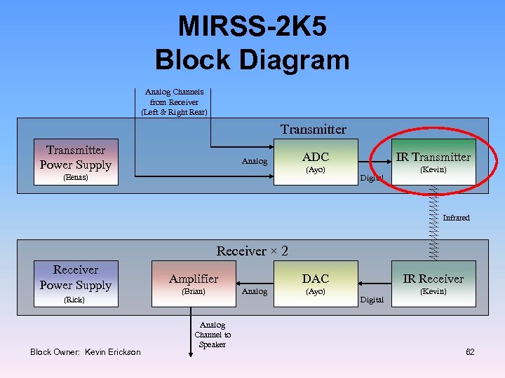
MIRSS-2 K 5 Block Diagram Analog Channels from Receiver (Left & Right Rear) Transmitter Power Supply Analog (Eenas) ADC (Ayo) IR Transmitter Digital (Kevin) Infrared Receiver × 2 Receiver Power Supply (Rick) Block Owner: Kevin Erickson Amplifier (Brian) Analog Channel to Speaker DAC Analog (Ayo) IR Receiver Digital (Kevin) 62
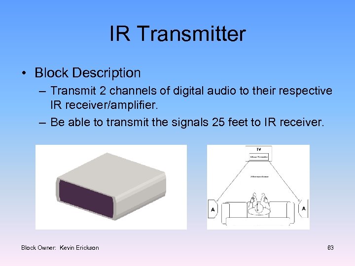
IR Transmitter • Block Description – Transmit 2 channels of digital audio to their respective IR receiver/amplifier. – Be able to transmit the signals 25 feet to IR receiver. Block Owner: Kevin Erickson 63
IR Transmitter Performance Requirements Power Inputs • 4. 75 – 5. 25 Volts DC Electrical Interfaces • Serial Digital Input from ADC block • Digital Infrared output to IR Receiver block – Infrared wavelength λ = 950 nm Block Owner: Kevin Erickson 64
IR Transmitter Standard Requirements PCB Circuit Area • 35 cm 2 Unique Parts • Infrared Emitter Temperature Ranges • Operating Temperatures: -40°C – 100°C Humidity Ranges • Operating humidity: 20% – 85% Safety • IEC 61603 – Transmission of audio and related signals using infrared radiation Block Owner: Kevin Erickson 65
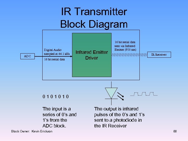
IR Transmitter Block Diagram ADC Digital Audio sampled at 44. 1 k. Hz 16 bit serial data Infrared Emitter Driver 16 bit serial data sent via Infrared Emitter (950 nm) IR Receiver 0 1 0 1 0 The input is a series of 0’s and 1’s from the ADC block. Block Owner: Kevin Erickson The output is infrared pulses of the 0’s and 1’s sent to a photodiode in the IR Receiver 66
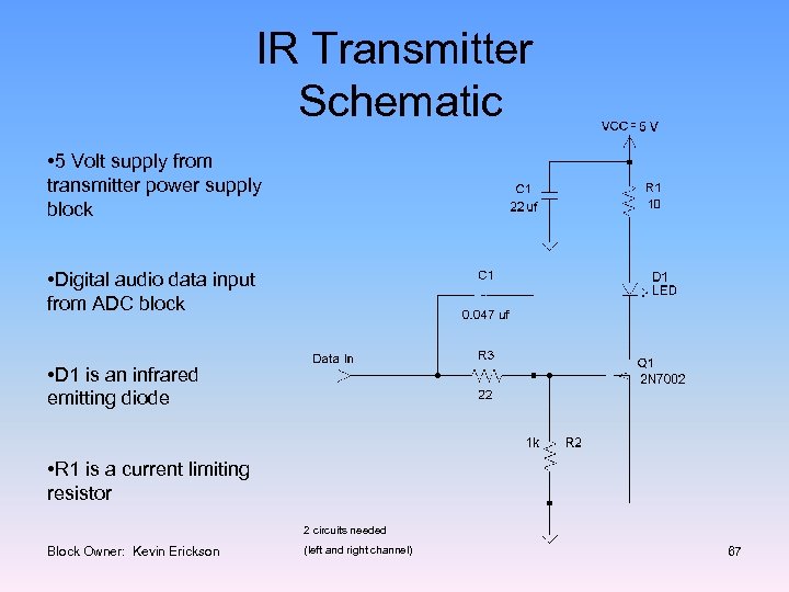
IR Transmitter Schematic • 5 Volt supply from transmitter power supply block • Digital audio data input from ADC block • D 1 is an infrared emitting diode • R 1 is a current limiting resistor 2 circuits needed Block Owner: Kevin Erickson (left and right channel) 67
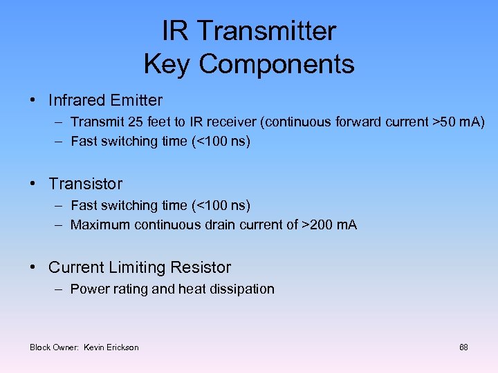
IR Transmitter Key Components • Infrared Emitter – Transmit 25 feet to IR receiver (continuous forward current >50 m. A) – Fast switching time (<100 ns) • Transistor – Fast switching time (<100 ns) – Maximum continuous drain current of >200 m. A • Current Limiting Resistor – Power rating and heat dissipation Block Owner: Kevin Erickson 68
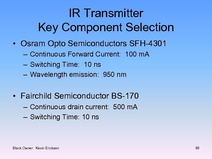
IR Transmitter Key Component Selection • Osram Opto Semiconductors SFH-4301 – Continuous Forward Current: 100 m. A – Switching Time: 10 ns – Wavelength emission: 950 nm • Fairchild Semiconductor BS-170 – Continuous drain current: 500 m. A – Switching Time: 10 ns Block Owner: Kevin Erickson 69
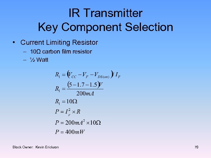
IR Transmitter Key Component Selection • Current Limiting Resistor – 10Ω carbon film resistor – ½ Watt Block Owner: Kevin Erickson 70
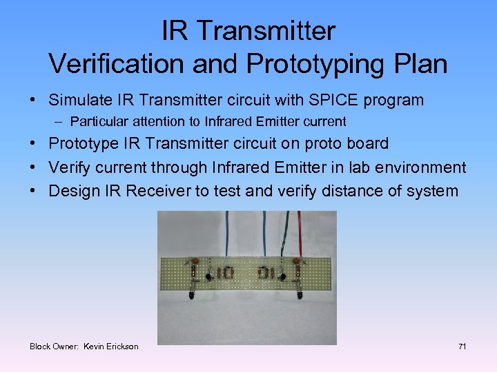
IR Transmitter Verification and Prototyping Plan • Simulate IR Transmitter circuit with SPICE program – Particular attention to Infrared Emitter current • Prototype IR Transmitter circuit on proto board • Verify current through Infrared Emitter in lab environment • Design IR Receiver to test and verify distance of system Block Owner: Kevin Erickson 71
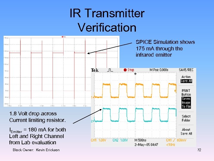
IR Transmitter Verification SPICE Simulation shows 175 m. A through the infrared emitter 1. 8 Volt drop across Current limiting resistor. IEmitter = 180 m. A for both Left and Right Channel from Lab evaluation Block Owner: Kevin Erickson 72
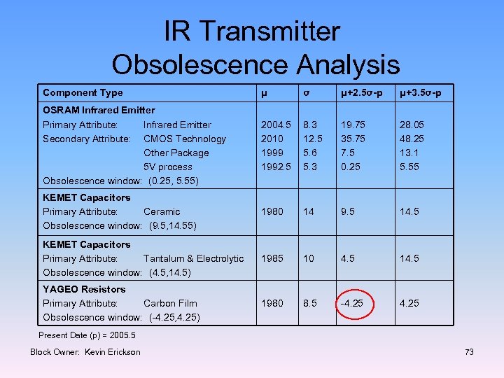
IR Transmitter Obsolescence Analysis Component Type μ σ μ+2. 5σ-p μ+3. 5σ-p OSRAM Infrared Emitter Primary Attribute: Infrared Emitter Secondary Attribute: CMOS Technology Other Package 5 V process Obsolescence window: (0. 25, 5. 55) 2004. 5 2010 1999 1992. 5 8. 3 12. 5 5. 6 5. 3 19. 75 35. 75 7. 5 0. 25 28. 05 48. 25 13. 1 5. 55 KEMET Capacitors Primary Attribute: Ceramic Obsolescence window: (9. 5, 14. 55) 1980 14 9. 5 14. 5 KEMET Capacitors Primary Attribute: Tantalum & Electrolytic Obsolescence window: (4. 5, 14. 5) 1985 10 4. 5 14. 5 YAGEO Resistors Primary Attribute: Carbon Film Obsolescence window: (-4. 25, 4. 25) 1980 8. 5 -4. 25 Present Date (p) = 2005. 5 Block Owner: Kevin Erickson 73
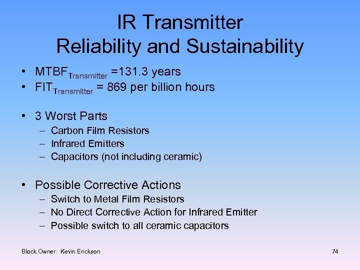
IR Transmitter Reliability and Sustainability • MTBFTransmitter =131. 3 years • FITTransmitter = 869 per billion hours • 3 Worst Parts – Carbon Film Resistors – Infrared Emitters – Capacitors (not including ceramic) • Possible Corrective Actions – Switch to Metal Film Resistors – No Direct Corrective Action for Infrared Emitter – Possible switch to all ceramic capacitors Block Owner: Kevin Erickson 74
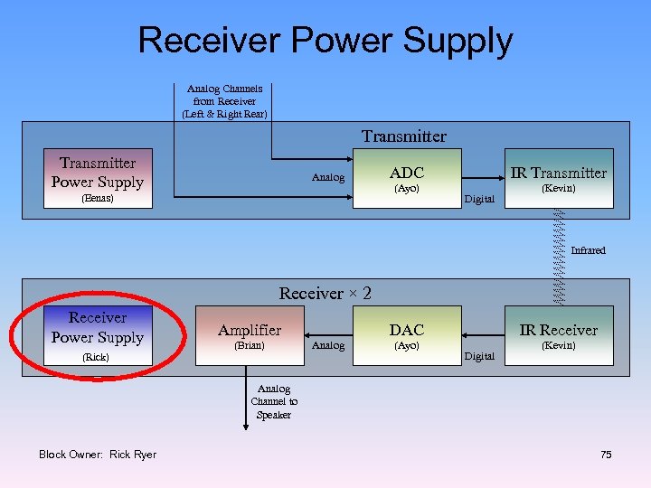
Receiver Power Supply Analog Channels from Receiver (Left & Right Rear) Transmitter Power Supply Analog (Eenas) ADC (Ayo) IR Transmitter Digital (Kevin) Infrared Receiver × 2 Receiver Power Supply (Rick) Amplifier (Brian) DAC Analog (Ayo) IR Receiver Digital (Kevin) Analog Channel to Speaker Block Owner: Rick Ryer 75
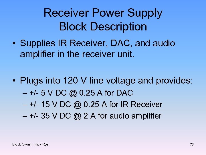
Receiver Power Supply Block Description • Supplies IR Receiver, DAC, and audio amplifier in the receiver unit. • Plugs into 120 V line voltage and provides: – +/- 5 V DC @ 0. 25 A for DAC – +/- 15 V DC @ 0. 25 A for IR Receiver – +/- 35 V DC @ 2 A for audio amplifier Block Owner: Rick Ryer 76
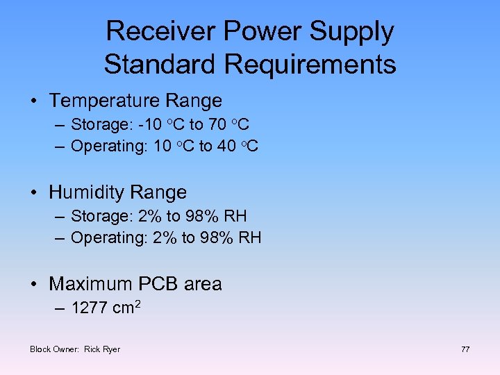
Receiver Power Supply Standard Requirements • Temperature Range – Storage: -10 o. C to 70 o. C – Operating: 10 o. C to 40 o. C • Humidity Range – Storage: 2% to 98% RH – Operating: 2% to 98% RH • Maximum PCB area – 1277 cm 2 Block Owner: Rick Ryer 77
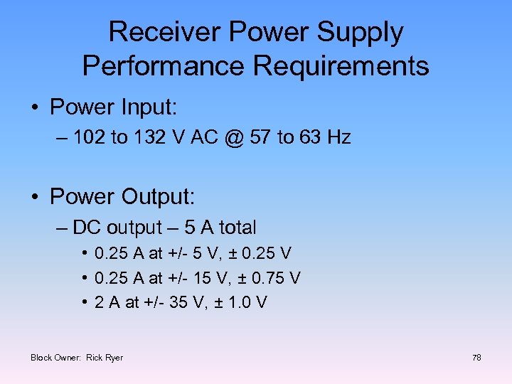
Receiver Power Supply Performance Requirements • Power Input: – 102 to 132 V AC @ 57 to 63 Hz • Power Output: – DC output – 5 A total • 0. 25 A at +/- 5 V, ± 0. 25 V • 0. 25 A at +/- 15 V, ± 0. 75 V • 2 A at +/- 35 V, ± 1. 0 V Block Owner: Rick Ryer 78
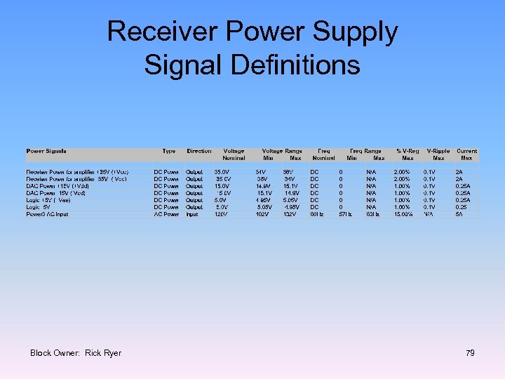
Receiver Power Supply Signal Definitions Block Owner: Rick Ryer 79
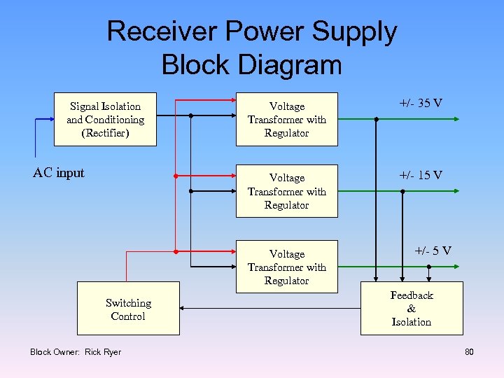
Receiver Power Supply Block Diagram AC input Voltage Transformer with Regulator +/- 35 V Voltage Transformer with Regulator Signal Isolation and Conditioning (Rectifier) +/- 15 V Voltage Transformer with Regulator Switching Control Block Owner: Rick Ryer +/- 5 V Feedback & Isolation 80
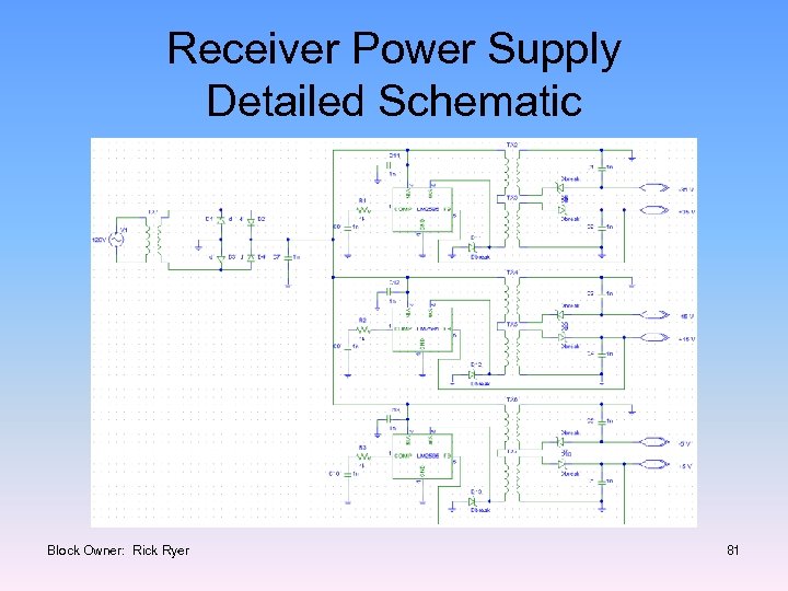
Receiver Power Supply Detailed Schematic Block Owner: Rick Ryer 81
Receiver Power Supply Schematic Notes • Voltage Regulators – +/- 5 V DC regulator uses LM 2585 – +/- 15 V DC regulator uses LM 2588 – +/- 35 V DC regulator uses LM 2587 • Implementation – Mostly Thru-Hole technology for prototype – Nearly all surface mount for product. Block Owner: Rick Ryer 82
Receiver Power Supply Block Attributes Block Location – This block will reside in a metal enclosure at the rear of the receiver package. – It will reside on its own circuit board within this enclosure. – Connection to other PCB will be made via heavy gauge wire and a connector Testing – This block requires no special testing other than verify the performance requirements. – Safety standard testing will rely on the success of the metal enclosure as shielding Block Owner: Rick Ryer 83
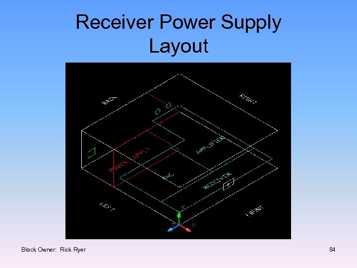
Receiver Power Supply Layout Block Owner: Rick Ryer 84
Receiver Power Supply Key Component Selection • Transformer – Must provide at least 70 VA power for audio amplifier (35 V at 2 A) – Must support 5 A on secondary windings • 35 V regulator – Must switch fast enough to sustain 70 W on output – Must provide +/- 35 V at output – Must accept +/- 18 V DC input (based on transformer specifications) Block Owner: Rick Ryer 85

Receiver Power Supply Lab Results • Transformers Block Owner: Rick Ryer 86

Receiver Power Supply Lab results • Regulators Block Owner: Rick Ryer 87
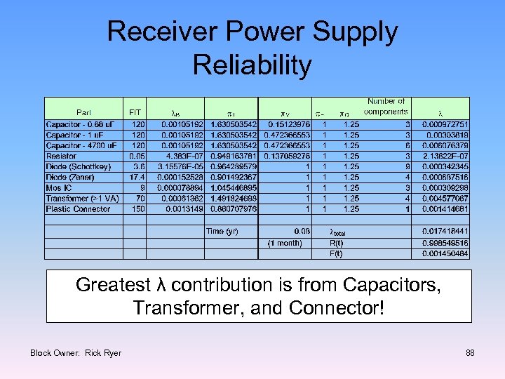
Receiver Power Supply Reliability Greatest λ contribution is from Capacitors, Transformer, and Connector! Block Owner: Rick Ryer 88
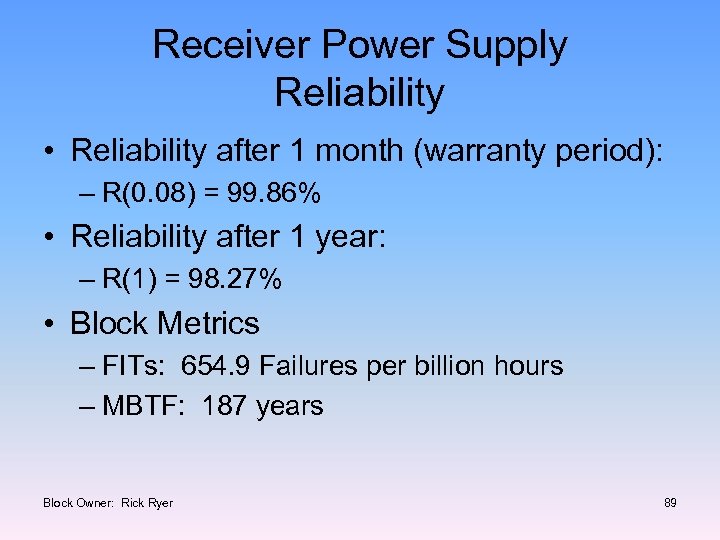
Receiver Power Supply Reliability • Reliability after 1 month (warranty period): – R(0. 08) = 99. 86% • Reliability after 1 year: – R(1) = 98. 27% • Block Metrics – FITs: 654. 9 Failures per billion hours – MBTF: 187 years Block Owner: Rick Ryer 89
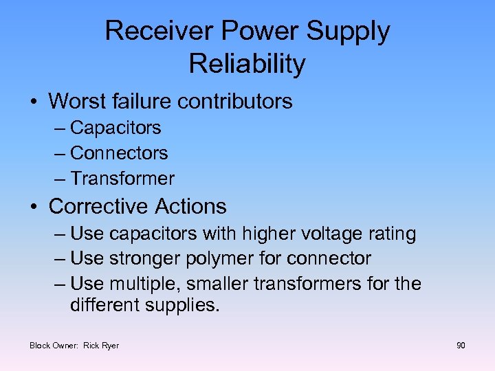
Receiver Power Supply Reliability • Worst failure contributors – Capacitors – Connectors – Transformer • Corrective Actions – Use capacitors with higher voltage rating – Use stronger polymer for connector – Use multiple, smaller transformers for the different supplies. Block Owner: Rick Ryer 90
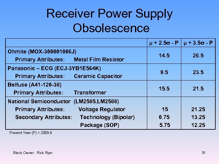
Receiver Power Supply Obsolescence µ + 2. 5σ - P µ + 3. 5σ - P Ohmite (MOX-300001006 J) Primary Attributes: Metal Film Resistor 14. 5 26. 5 Panasonic – ECG (ECJ-3 YB 1 E 564 K) Primary Attributes: Ceramic Capacitor 9. 5 23. 5 Belfuse (A 41 -120 -38) Primary Attributes: 15. 5 21. 5 15 0. 75 5. 75 21. 25 13. 25 12. 25 Transformer National Semiconductor (LM 2585, LM 2588) Primary Attributes: Voltage Regulator Secondary Attributes: Technology (Bipolar) Package (SOP) Present Year (P) = 2005. 5 Block Owner: Rick Ryer 91
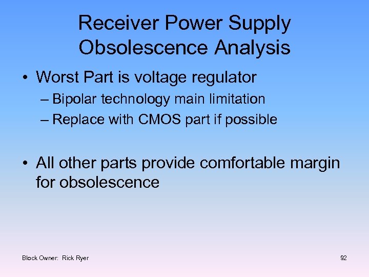
Receiver Power Supply Obsolescence Analysis • Worst Part is voltage regulator – Bipolar technology main limitation – Replace with CMOS part if possible • All other parts provide comfortable margin for obsolescence Block Owner: Rick Ryer 92
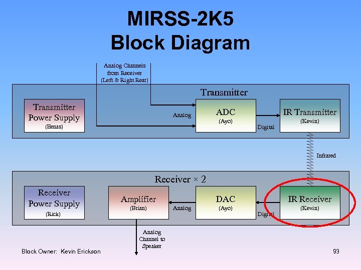
MIRSS-2 K 5 Block Diagram Analog Channels from Receiver (Left & Right Rear) Transmitter Power Supply Analog (Eenas) ADC (Ayo) IR Transmitter Digital (Kevin) Infrared Receiver × 2 Receiver Power Supply (Rick) Block Owner: Kevin Erickson Amplifier (Brian) Analog Channel to Speaker DAC Analog (Ayo) IR Receiver Digital (Kevin) 93
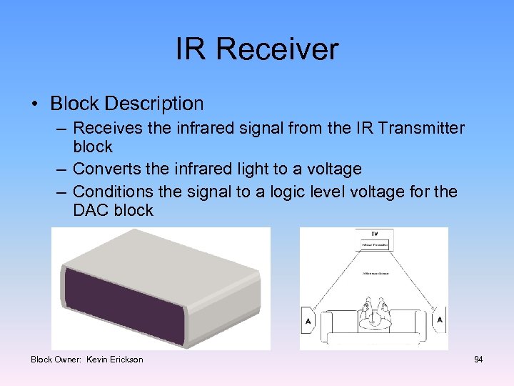
IR Receiver • Block Description – Receives the infrared signal from the IR Transmitter block – Converts the infrared light to a voltage – Conditions the signal to a logic level voltage for the DAC block Block Owner: Kevin Erickson 94
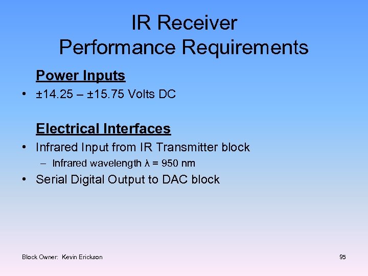
IR Receiver Performance Requirements Power Inputs • ± 14. 25 – ± 15. 75 Volts DC Electrical Interfaces • Infrared Input from IR Transmitter block – Infrared wavelength λ = 950 nm • Serial Digital Output to DAC block Block Owner: Kevin Erickson 95
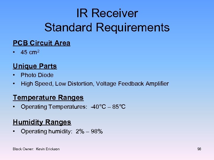
IR Receiver Standard Requirements PCB Circuit Area • 45 cm 2 Unique Parts • Photo Diode • High Speed, Low Distortion, Voltage Feedback Amplifier Temperature Ranges • Operating Temperatures: -40°C – 85°C Humidity Ranges • Operating humidity: 2% – 98% Block Owner: Kevin Erickson 96
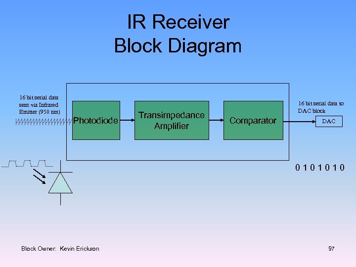
IR Receiver Block Diagram 16 bit serial data sent via Infrared Emitter (950 nm) Photodiode Transimpedance Amplifier 16 bit serial data to DAC block Comparator DAC 0 1 0 1 0 Block Owner: Kevin Erickson 97
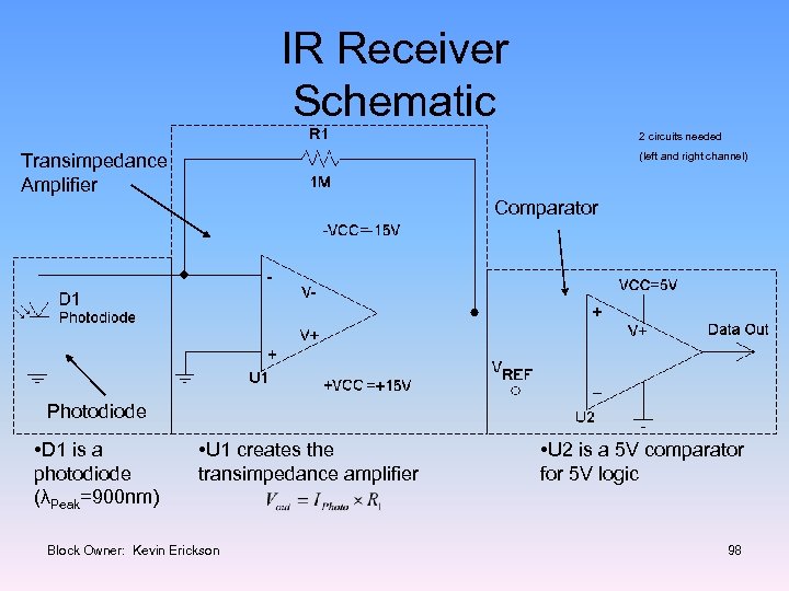
IR Receiver Schematic 2 circuits needed Transimpedance Amplifier (left and right channel) Comparator Photodiode • D 1 is a photodiode (λPeak=900 nm) • U 1 creates the transimpedance amplifier Block Owner: Kevin Erickson • U 2 is a 5 V comparator for 5 V logic 98
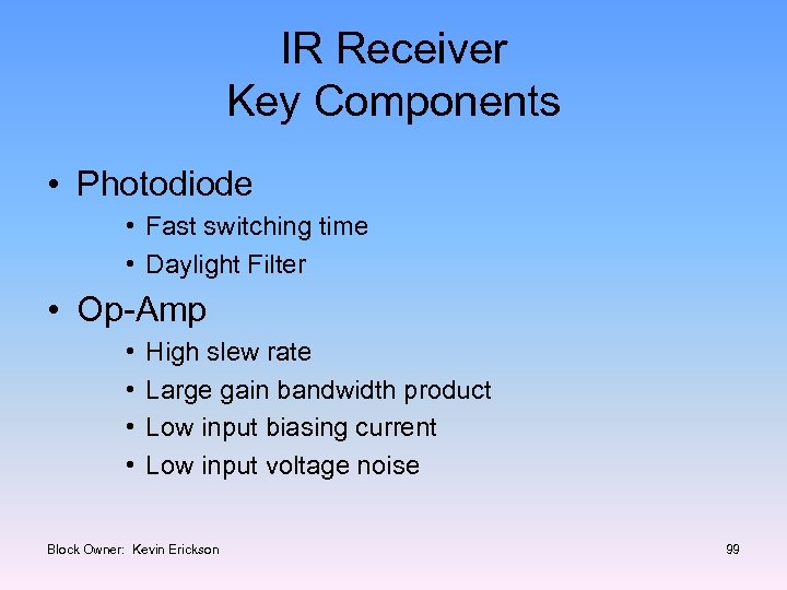
IR Receiver Key Components • Photodiode • Fast switching time • Daylight Filter • Op-Amp • • High slew rate Large gain bandwidth product Low input biasing current Low input voltage noise Block Owner: Kevin Erickson 99
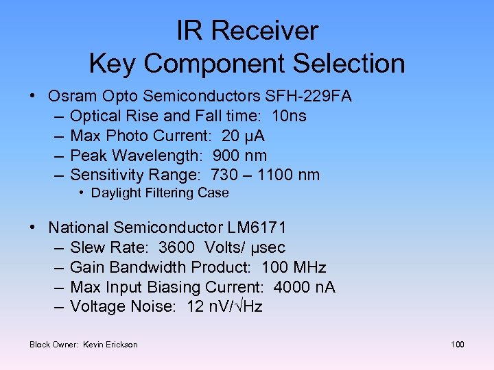
IR Receiver Key Component Selection • Osram Opto Semiconductors SFH-229 FA – Optical Rise and Fall time: 10 ns – Max Photo Current: 20 μA – Peak Wavelength: 900 nm – Sensitivity Range: 730 – 1100 nm • Daylight Filtering Case • National Semiconductor LM 6171 – Slew Rate: 3600 Volts/ μsec – Gain Bandwidth Product: 100 MHz – Max Input Biasing Current: 4000 n. A – Voltage Noise: 12 n. V/√Hz Block Owner: Kevin Erickson 100
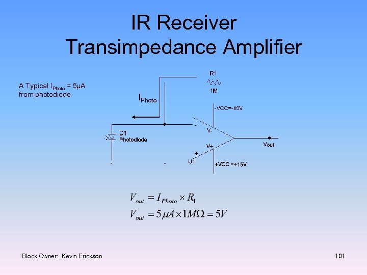
IR Receiver Transimpedance Amplifier A Typical IPhoto = 5μA from photodiode Block Owner: Kevin Erickson IPhoto 101
IR Receiver Prototyping and Verification Plan • Prototype IR Receiver circuit(s) on proto board • Set up IR Transmitter to transmit 1 k. Hz 0 -5 Volt square wave – Observe that the IR Receiver works under short distances – Lengthen the distance between the IR Transmitter and IR Receiver and observe the output of the amplifier – Speed up IR Transmitter to 1 MHz • Explore other Photodiode circuits to meet distance and/or speed requirements Block Owner: Kevin Erickson 102
IR Receiver Verification • Suggested screen captures – Output of op-amp • Digital Photo showing distance of transmission Block Owner: Kevin Erickson 103
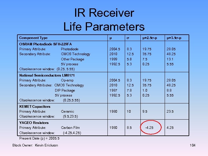
IR Receiver Life Parameters Component Type μ σ μ+2. 5σ-p μ+3. 5σ-p OSRAM Photodiode SFH-229 FA Primary Attribute: Photodiode Secondary Attribute: CMOS Technology Other Package 5 V process Obsolescence window: (0. 25, 5. 55) 2004. 5 2010 1999 1992. 5 8. 3 12. 5 5. 6 5. 3 19. 75 35. 75 7. 5 0. 25 28. 05 48. 25 13. 1 5. 55 National Semiconductors LM 6171 Primary Attribute: Op-amp Secondary Attributes: CMOS Technology DIP Package 5 V process Obsolescence window: (0. 25, 5. 55) 2004. 5 2010 1987 1992. 5 8. 3 12. 5 7. 8 5. 3 19. 75 35. 75 1. 0 0. 25 28. 05 48. 25 8. 8 5. 55 KEMET Capacitors Primary Attribute: Obsolescence window: Ceramic (9. 5, 23. 5) 1980 10 9. 5 23. 5 YAGEO Resistors Primary Attribute: Obsolescence window: Carbon Film (-4. 25, 4. 25) 1980 8. 5 -4. 25 Present Date (p) = 2005. 5 Block Owner: Kevin Erickson 104
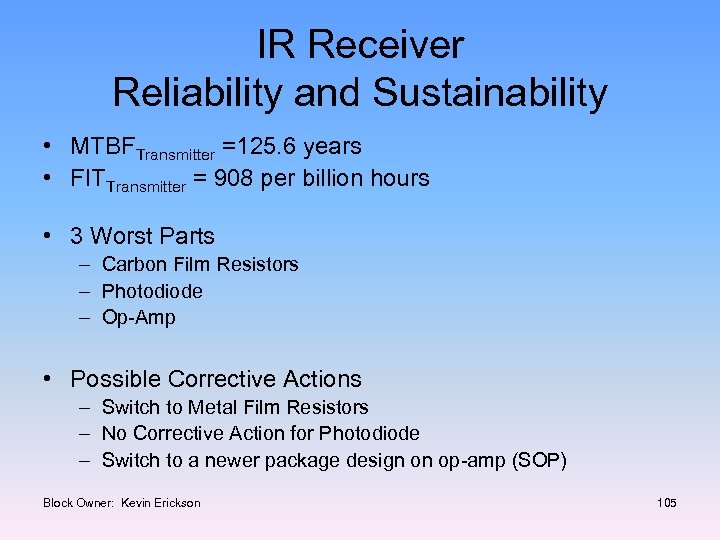
IR Receiver Reliability and Sustainability • MTBFTransmitter =125. 6 years • FITTransmitter = 908 per billion hours • 3 Worst Parts – Carbon Film Resistors – Photodiode – Op-Amp • Possible Corrective Actions – Switch to Metal Film Resistors – No Corrective Action for Photodiode – Switch to a newer package design on op-amp (SOP) Block Owner: Kevin Erickson 105
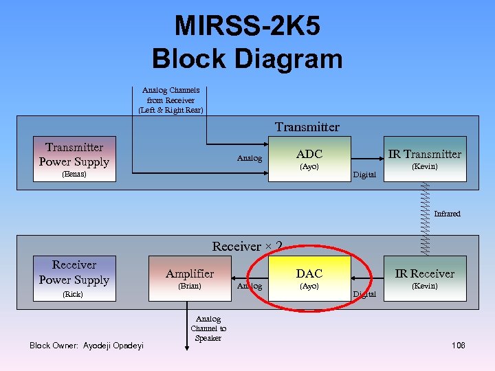
MIRSS-2 K 5 Block Diagram Analog Channels from Receiver (Left & Right Rear) Transmitter Power Supply Analog (Eenas) ADC (Ayo) IR Transmitter Digital (Kevin) Infrared Receiver × 2 Receiver Power Supply (Rick) Block Owner: Ayodeji Opadeyi Amplifier (Brian) Analog Channel to Speaker DAC Analog (Ayo) IR Receiver Digital (Kevin) 106
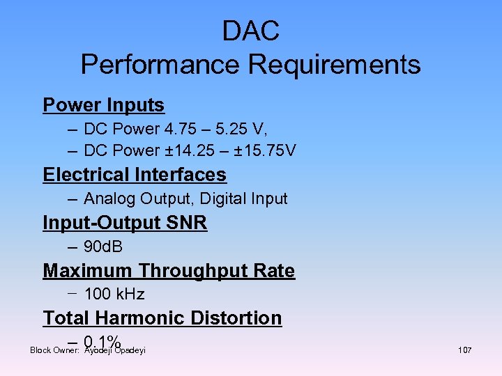
DAC Performance Requirements Power Inputs – DC Power 4. 75 – 5. 25 V, – DC Power ± 14. 25 – ± 15. 75 V Electrical Interfaces – Analog Output, Digital Input-Output SNR – 90 d. B Maximum Throughput Rate − 100 k. Hz Total Harmonic Distortion – 0. 1% Block Owner: Ayodeji Opadeyi 107
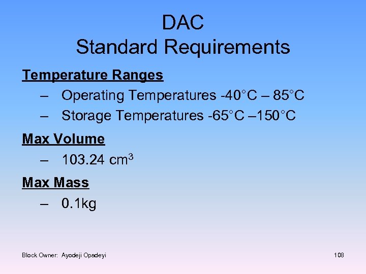
DAC Standard Requirements Temperature Ranges – Operating Temperatures -40°C – 85°C – Storage Temperatures -65°C – 150°C Max Volume – 103. 24 cm 3 Max Mass – 0. 1 kg Block Owner: Ayodeji Opadeyi 108
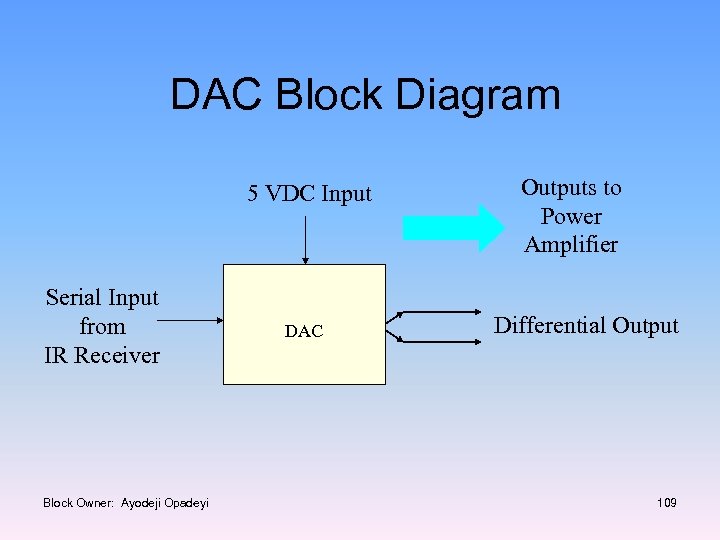
DAC Block Diagram 5 VDC Input Serial Input from IR Receiver Block Owner: Ayodeji Opadeyi DAC Outputs to Power Amplifier Differential Output 109
DAC Key Components • Eight 5% resistors ½ W – For restoring the signal to its original form • two op-amps – Amplifying the signal to its original amplitude – Low noise, high speed amplifiers • 2 Max 542 chips (Surface mount) – Converts the digital signal back to analog – 16 Bit serial input Block Owner: Ayodeji Opadeyi 110
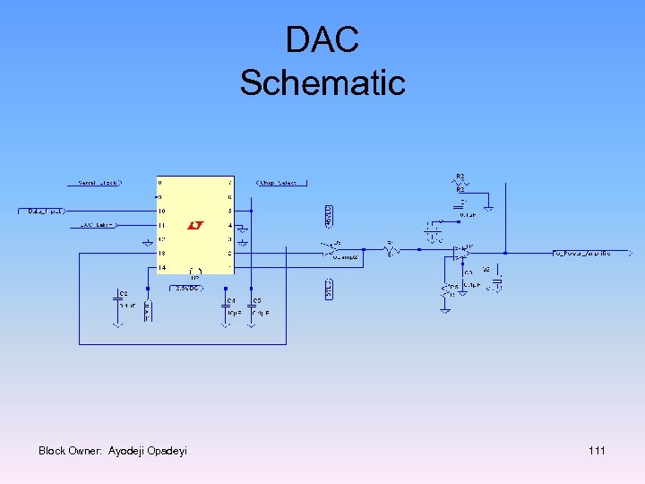
DAC Schematic Block Owner: Ayodeji Opadeyi 111
DAC Resistor Selection • The resistors were chosen to reverse the attenuation caused by the ADC signal reduction, but it had to be amplified by 2 because the reference voltage of the ADC is 5 V, and that of the DAC is 2. 5 V. • R 1 = 20 kΩ • R 2 = 3. 9 kΩ • R 5 = R 1 || R 2 ≈ 3. 3 k Ω Block Owner: Ayodeji Opadeyi 112
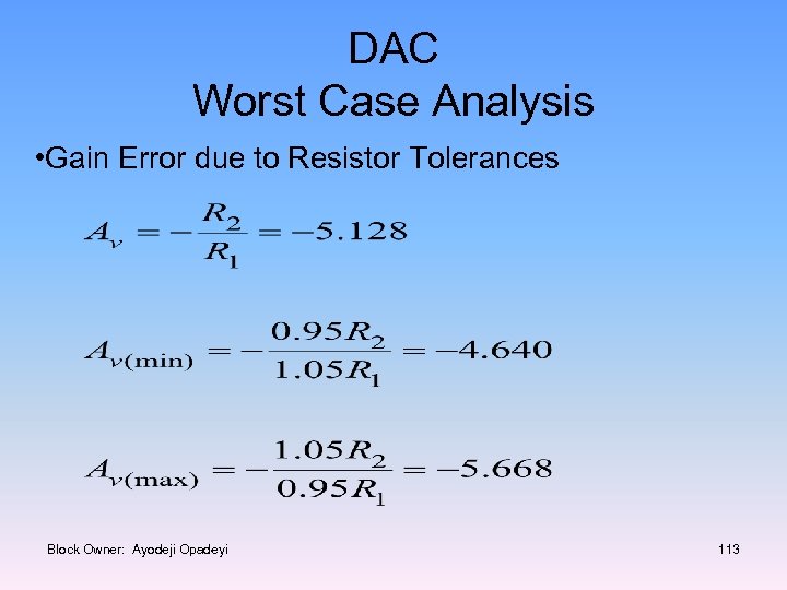
DAC Worst Case Analysis • Gain Error due to Resistor Tolerances Block Owner: Ayodeji Opadeyi 113
DAC Block Reliability • Block FITs: – 571. 3 failure Units per billion hours • MTBF: – 199. 7 years • Most unreliable parts – DAC, and Capacitors • Solution to improve the reliability – Use more reliable capacitors – DAC cannot be changed. Block Owner: Ayodeji Opadeyi 114
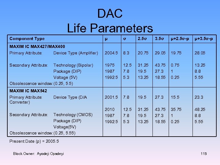
DAC Life Parameters Component Type μ σ 2. 5σ 3. 5σ μ+2. 5σ-p μ+3. 5σ-p MAXIM IC MAX 427/MAX 400 Primary Attribute: Device Type (Amplifier) 2004. 5 8. 3 20. 75 29. 05 19. 75 28. 05 Secondary Attribute: Technology (Bipolar) Package (DIP) Voltage (5 V) Obsolescence window: (0. 25, 5. 5) 1975 1987 1992. 5 12. 5 7. 8 5. 3 31. 25 19. 5 13. 25 43. 75 27. 3 18. 55 0. 75 1 0. 25 13. 25 8. 8 5. 55 2001. 5 7. 8 19. 5 27. 3 15. 5 23. 3 2010 1987 1992. 5 12. 5 7. 8 5. 3 31. 25 19. 5 13. 25 43. 75 27. 3 18. 55 35. 75 1 0. 25 48. 25 8. 8 5. 55 MAXIM IC MAX 542 Primary Attribute: Converter) Device Type (D/A Secondary Attribute: Technology (CMOS) Package (DIP) Voltage(5 V) Obsolescence window: (0. 25, 5. 55) Present Date (p) = 2005. 5 Block Owner: Ayodeji Opadeyi 115
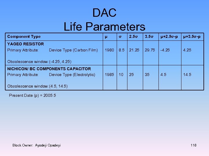
DAC Life Parameters Component Type YAGEO RESISTOR Primary Attribute: μ Device Type (Carbon Film) σ 2. 5σ 3. 5σ μ+2. 5σ-p μ+3. 5σ-p 1980 8. 5 21. 25 29. 75 -4. 25 1985 10 25 35 4. 5 14. 5 Obsolescence window: (-4. 25, 4. 25) NICHICON/ BC COMPONENTS CAPACITOR Primary Attribute: Device Type (Electrolytic) Obsolescence window: (4. 5, 14. 5) Present Date (p) = 2005. 5 Block Owner: Ayodeji Opadeyi 116
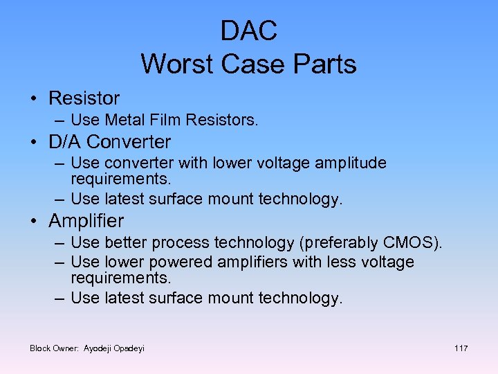
DAC Worst Case Parts • Resistor – Use Metal Film Resistors. • D/A Converter – Use converter with lower voltage amplitude requirements. – Use latest surface mount technology. • Amplifier – Use better process technology (preferably CMOS). – Use lower powered amplifiers with less voltage requirements. – Use latest surface mount technology. Block Owner: Ayodeji Opadeyi 117
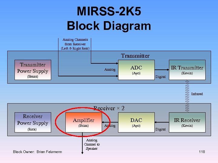
MIRSS-2 K 5 Block Diagram Analog Channels from Receiver (Left & Right Rear) Transmitter Power Supply Analog (Eenas) ADC (Ayo) IR Transmitter Digital (Kevin) Infrared Receiver × 2 Receiver Power Supply (Rick) Block Owner: Brian Felsmenn Amplifier (Brian) Analog Channel to Speaker DAC Analog (Ayo) IR Receiver Digital (Kevin) 118
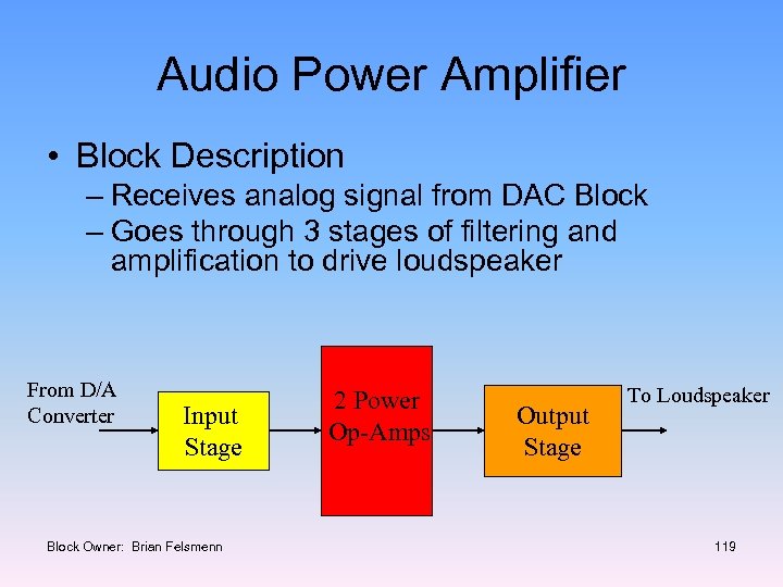
Audio Power Amplifier • Block Description – Receives analog signal from DAC Block – Goes through 3 stages of filtering and amplification to drive loudspeaker From D/A Converter Input Stage Block Owner: Brian Felsmenn 2 Power Op-Amps Output Stage To Loudspeaker 119
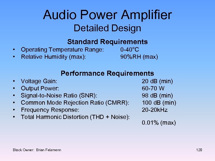
Audio Power Amplifier Detailed Design Standard Requirements • Operating Temperature Range: • Relative Humidity (max): 0 -40°C 90%RH (max) Performance Requirements • • • Voltage Gain: Output Power: Signal-to-Noise Ratio (SNR): Common Mode Rejection Ratio (CMRR): Frequency Response: Total Harmonic Distortion (THD + Noise): Block Owner: Brian Felsmenn 20 d. B (min) 60 -70 W 98 d. B (min) 100 d. B (min) 20 -20 k. Hz 0. 01% (max) 120
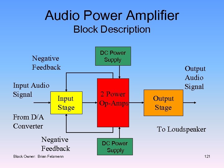
Audio Power Amplifier Block Description Negative Feedback Input Audio Signal Input Stage DC Power Supply 2 Power Op-Amps From D/A Converter Negative Feedback Block Owner: Brian Felsmenn Output Audio Signal Output Stage To Loudspeaker DC Power Supply 121
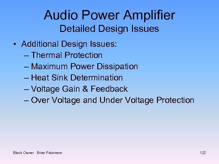
Audio Power Amplifier Detailed Design Issues • Additional Design Issues: – Thermal Protection – Maximum Power Dissipation – Heat Sink Determination – Voltage Gain & Feedback – Over Voltage and Under Voltage Protection Block Owner: Brian Felsmenn 122
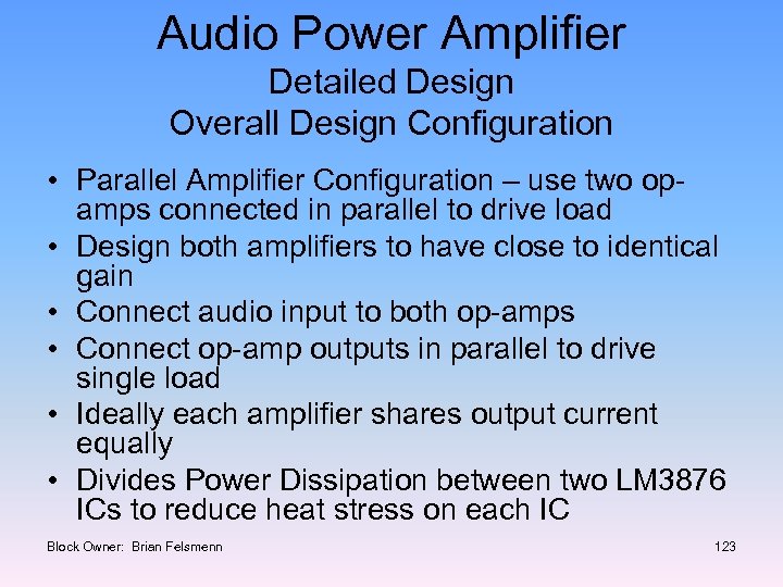
Audio Power Amplifier Detailed Design Overall Design Configuration • Parallel Amplifier Configuration – use two opamps connected in parallel to drive load • Design both amplifiers to have close to identical gain • Connect audio input to both op-amps • Connect op-amp outputs in parallel to drive single load • Ideally each amplifier shares output current equally • Divides Power Dissipation between two LM 3876 ICs to reduce heat stress on each IC Block Owner: Brian Felsmenn 123
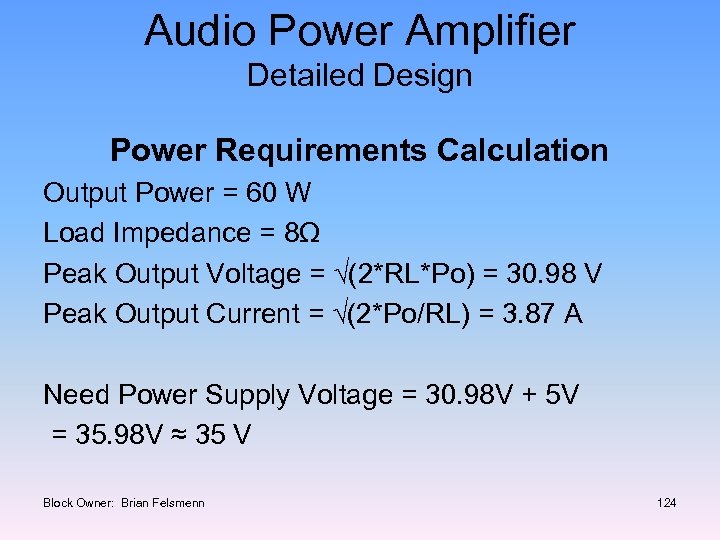
Audio Power Amplifier Detailed Design Power Requirements Calculation Output Power = 60 W Load Impedance = 8Ω Peak Output Voltage = √(2*RL*Po) = 30. 98 V Peak Output Current = √(2*Po/RL) = 3. 87 A Need Power Supply Voltage = 30. 98 V + 5 V = 35. 98 V ≈ 35 V Block Owner: Brian Felsmenn 124
Audio Power Amplifier Detailed Design Op-Amp and Feedback Design & Calculations • Non-inverting op-amp configuration with negative feedback • R 4 and R 6 set the gain of op-amp • Gain (nominal) = R 6/R 4 + 1 = 20 kΩ/1 kΩ +1 =21 • Gain (nominal) = 20 log(21) = 26 d. B Block Owner: Brian Felsmenn 125
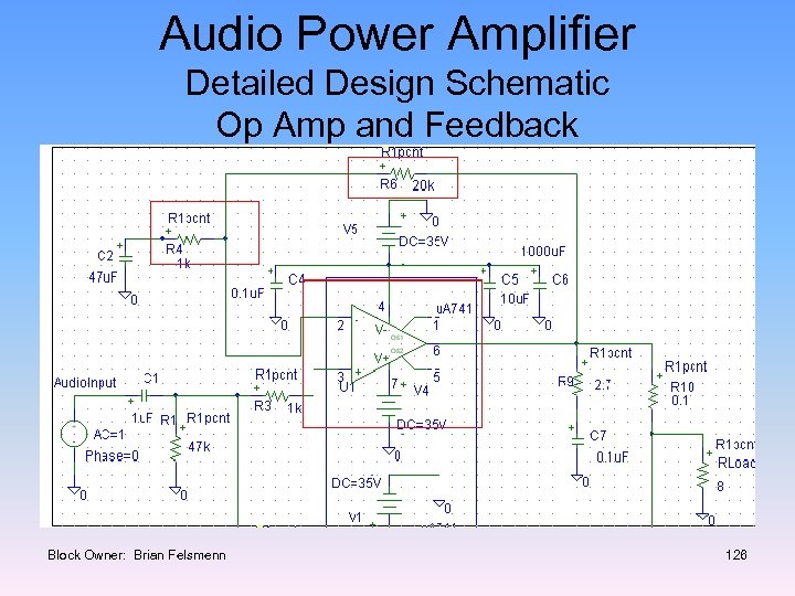
Audio Power Amplifier Detailed Design Schematic Op Amp and Feedback Block Owner: Brian Felsmenn 126
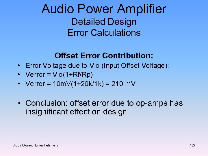
Audio Power Amplifier Detailed Design Error Calculations Offset Error Contribution: • Error Voltage due to Vio (Input Offset Voltage): • Verror = Vio(1+Rf/Rp) • Verror = 10 m. V(1+20 k/1 k) = 210 m. V • Conclusion: offset error due to op-amps has insignificant effect on design Block Owner: Brian Felsmenn 127
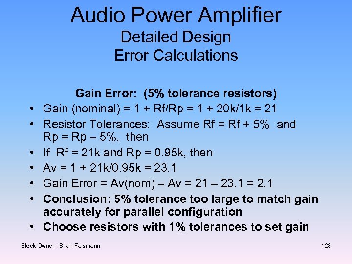
Audio Power Amplifier Detailed Design Error Calculations • • Gain Error: (5% tolerance resistors) Gain (nominal) = 1 + Rf/Rp = 1 + 20 k/1 k = 21 Resistor Tolerances: Assume Rf = Rf + 5% and Rp = Rp – 5%, then If Rf = 21 k and Rp = 0. 95 k, then Av = 1 + 21 k/0. 95 k = 23. 1 Gain Error = Av(nom) – Av = 21 – 23. 1 = 2. 1 Conclusion: 5% tolerance too large to match gain accurately for parallel configuration Choose resistors with 1% tolerances to set gain Block Owner: Brian Felsmenn 128
Audio Power Amplifier Detailed Design Error Calculations Gain Error (1% tolerance resistors) • Gain (nominal) = 1 + Rf/Rp = 1 + 20 k/1 k = 21 • Resistor Tolerances: Assume Rf = Rf + 1% and Rp = Rp – 1% then • Rf = 20. 2 k and Rp = 0. 99 k • Then Av = 1 + Rf/Rp = 1 + 20. 2 k/0. 99 k = 21. 4 • Gain Error = Av(nom) – Av = 21 – 21. 4 = 0. 4 • Conclusion: 1% resistors offer much better gain error and matching for parallel amplifier configuration Block Owner: Brian Felsmenn 129
Audio Power Amplifier Detailed Design Input Stage Design Calculations: Need high-pass filter to prevent oscillations: • R 1 and C 1 create a high-pass filter: • Choose R 1 = 47 kΩ and C 1= 1μF • So F = 1/(2π*R 1*C 1) = 3. 38 Hz (cut-off freq) • C 1 is also a coupling capacitor Need high-pass filter on feedback loop for unity gain at DC: • R 4 and C 2 create a high-pass filter: • Choose R 4 = 1 kΩ and C 2 = 47μF • So F = 1/(2π*R 4*C 2) = 3. 38 Hz (cut-off freq) • R 4 is also a gain determining resistor Block Owner: Brian Felsmenn 130
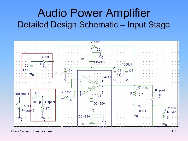
Audio Power Amplifier Detailed Design Schematic – Input Stage Block Owner: Brian Felsmenn 131

Audio Power Amplifier Detailed Design Power Supply Input Circuit Design • Power Supply and Filtering Capacitors • Capacitors C 4, C 5 and C 6 provide power supply filtering and bypassing • Need filtering and bypassing capacitors to smooth out any power supply ripple voltages and DC voltage to op-amps will remain constant Block Owner: Brian Felsmenn 132
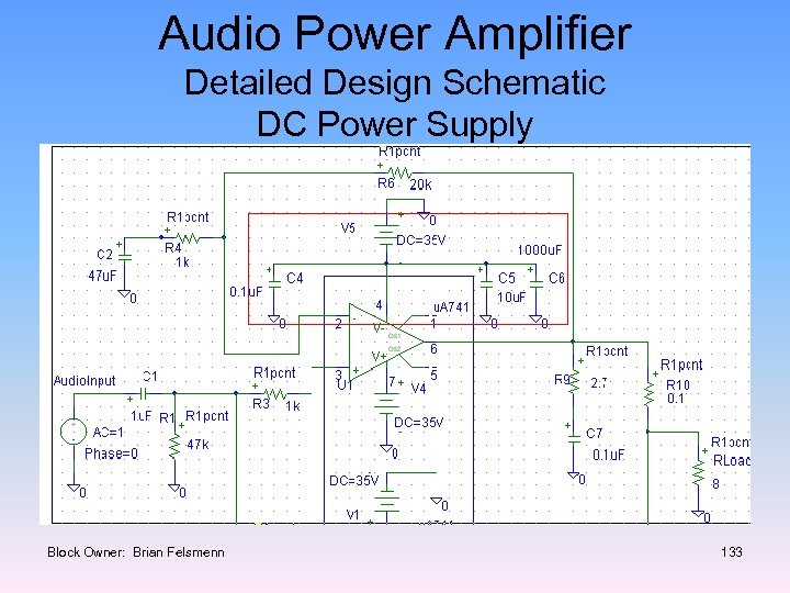
Audio Power Amplifier Detailed Design Schematic DC Power Supply Block Owner: Brian Felsmenn 133
Audio Power Amplifier Detailed Design Output Stage Design & Calculations: Need to stabilize output stage with a pole that reduces high frequency instabilities • R 9 and C 7 create a high frequency pole: • Choose R 9 = 2. 7Ω and C 7 = 0. 1μF • F = 1/(2π*R 9*C 7) = 5. 89 MHz • R 10 balances current to loudspeaker caused by gain or DC offset differences between op-amps • Choose R 10 = 0. 1Ω (3 W power rating) Block Owner: Brian Felsmenn 134
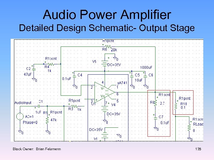
Audio Power Amplifier Detailed Design Schematic- Output Stage Block Owner: Brian Felsmenn 135
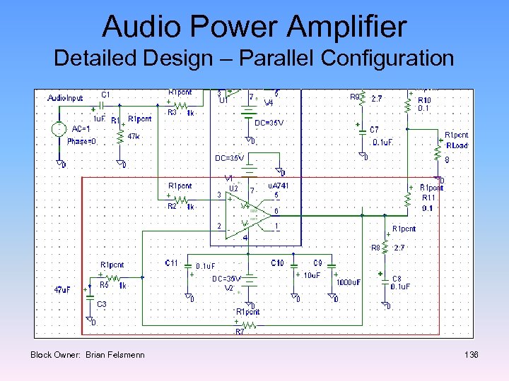
Audio Power Amplifier Detailed Design – Parallel Configuration Block Owner: Brian Felsmenn 136
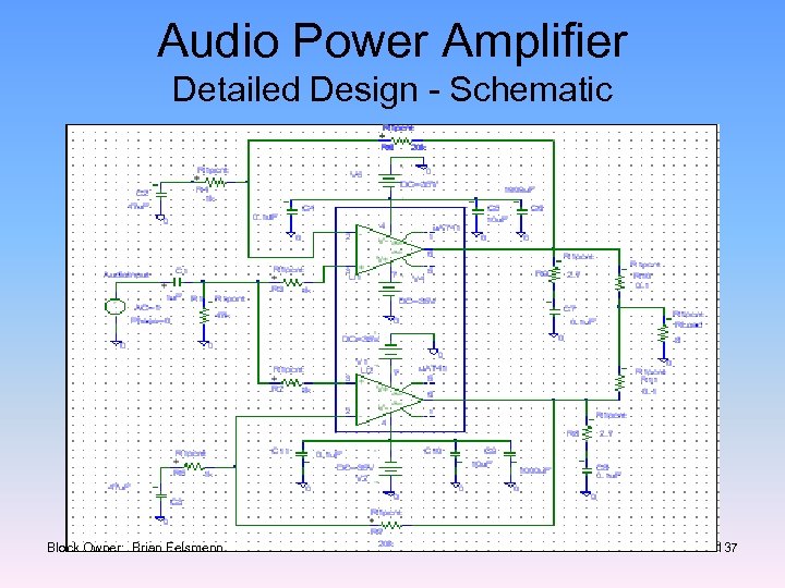
Audio Power Amplifier Detailed Design - Schematic Block Owner: Brian Felsmenn 137
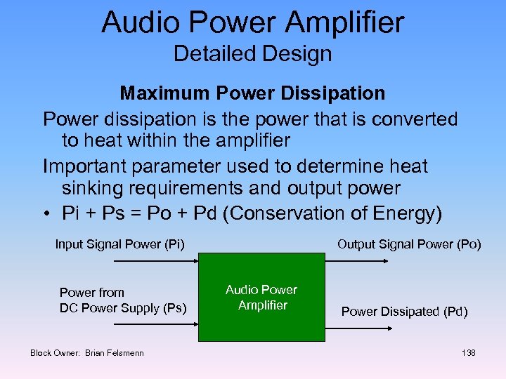
Audio Power Amplifier Detailed Design Maximum Power Dissipation Power dissipation is the power that is converted to heat within the amplifier Important parameter used to determine heat sinking requirements and output power • Pi + Ps = Po + Pd (Conservation of Energy) Input Signal Power (Pi) Power from DC Power Supply (Ps) Block Owner: Brian Felsmenn Output Signal Power (Po) Audio Power Amplifier Power Dissipated (Pd) 138
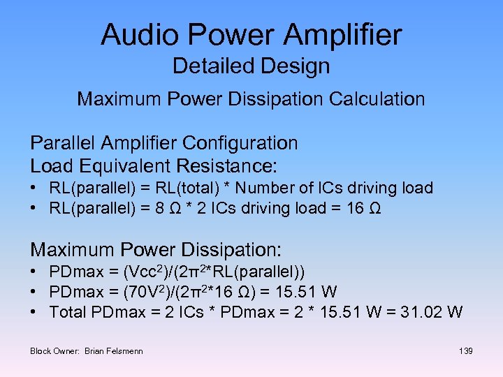
Audio Power Amplifier Detailed Design Maximum Power Dissipation Calculation Parallel Amplifier Configuration Load Equivalent Resistance: • RL(parallel) = RL(total) * Number of ICs driving load • RL(parallel) = 8 Ω * 2 ICs driving load = 16 Ω Maximum Power Dissipation: • PDmax = (Vcc 2)/(2π2*RL(parallel)) • PDmax = (70 V 2)/(2π2*16 Ω) = 15. 51 W • Total PDmax = 2 ICs * PDmax = 2 * 15. 51 W = 31. 02 W Block Owner: Brian Felsmenn 139
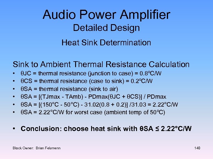
Audio Power Amplifier Detailed Design Heat Sink Determination Sink to Ambient Thermal Resistance Calculation • • • θJC = thermal resistance (junction to case) = 0. 8ºC/W θCS = thermal resistance (case to sink) = 0. 2ºC/W θSA = thermal resistance (sink to air) θSA = [(TJmax - TAmb) - PDmax(θJC + θCS)] / PDmax θSA = [(150°C - 50°C) - 31. 02(0. 8 + 0. 2)] /31. 03 = 2. 22°C/W θSA = 2. 22°C/W for worst case (ambient temp of 50ºC) • Conclusion: choose heat sink with θSA ≤ 2. 22°C/W Block Owner: Brian Felsmenn 140
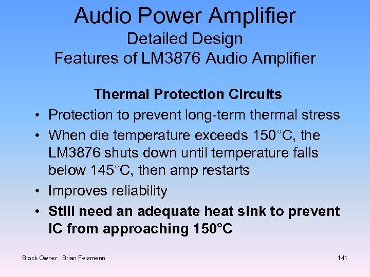
Audio Power Amplifier Detailed Design Features of LM 3876 Audio Amplifier • • Thermal Protection Circuits Protection to prevent long-term thermal stress When die temperature exceeds 150°C, the LM 3876 shuts down until temperature falls below 145°C, then amp restarts Improves reliability Still need an adequate heat sink to prevent IC from approaching 150°C Block Owner: Brian Felsmenn 141

Audio Power Amplifier Features of LM 3876 Audio Amplifier Device Protection • Under-Voltage Protection of LM 3876 built in protection allows power supplies and voltage across capacitors to reach full values before amp turned on to prevent DC output spikes • Over-Voltage Protection of LM 3876 built in protection limits the output current while providing voltage clamping Block Owner: Brian Felsmenn 142
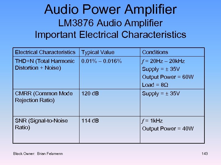
Audio Power Amplifier LM 3876 Audio Amplifier Important Electrical Characteristics Typical Value Conditions THD+N (Total Harmonic 0. 01% – 0. 016% Distortion + Noise) f = 20 Hz – 20 k. Hz Supply = ± 35 V Output Power = 60 W Load = 8Ω CMRR (Common Mode Rejection Ratio) 120 d. B Supply = ± 35 V SNR (Signal-to-Noise Ratio) 114 d. B f = 1 k. Hz Output Power = 40 W Block Owner: Brian Felsmenn 143
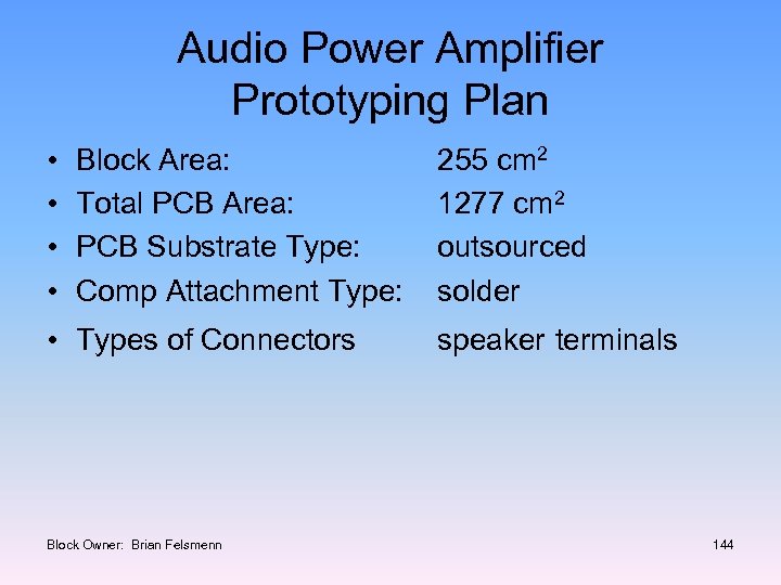
Audio Power Amplifier Prototyping Plan • • Block Area: Total PCB Area: PCB Substrate Type: Comp Attachment Type: • Types of Connectors Block Owner: Brian Felsmenn 255 cm 2 1277 cm 2 outsourced solder speaker terminals 144
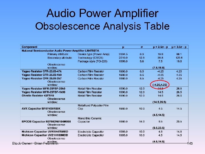
Audio Power Amplifier Obsolescence Analysis Table Block Owner: Brian Felsmenn 145
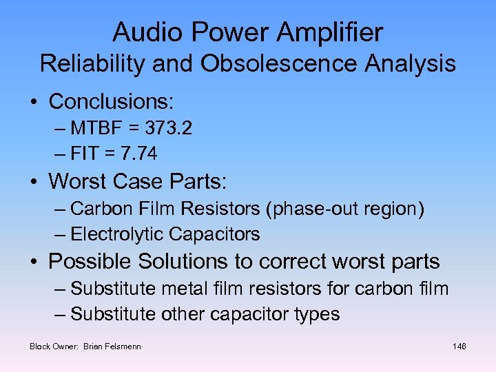
Audio Power Amplifier Reliability and Obsolescence Analysis • Conclusions: – MTBF = 373. 2 – FIT = 7. 74 • Worst Case Parts: – Carbon Film Resistors (phase-out region) – Electrolytic Capacitors • Possible Solutions to correct worst parts – Substitute metal film resistors for carbon film – Substitute other capacitor types Block Owner: Brian Felsmenn 146
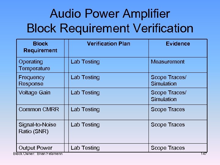
Audio Power Amplifier Block Requirement Verification Plan Evidence Operating Temperature Lab Testing Measurement Frequency Response Lab Testing Scope Traces/ Simulation Voltage Gain Lab Testing Scope Traces/ Simulation Common CMRR Lab Testing Scope Traces Signal-to-Noise Ratio (SNR) Lab Testing Scope Traces Output Power Lab Testing Scope Traces Block Owner: Brian Felsmenn 147
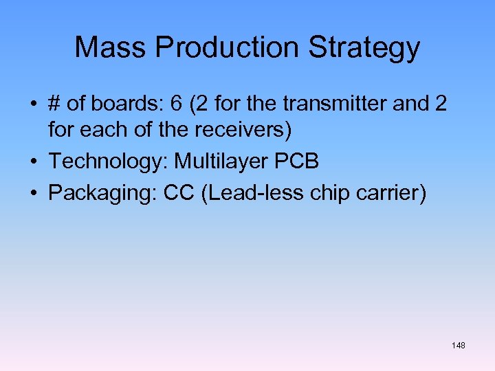
Mass Production Strategy • # of boards: 6 (2 for the transmitter and 2 for each of the receivers) • Technology: Multilayer PCB • Packaging: CC (Lead-less chip carrier) 148

Mass Production Parts List • Primarily Surface Mount parts • A few through hole components (Power Supply parts) • Pb-Free devices • Automated circuit board production 149
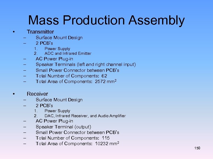
Mass Production Assembly • Transmitter – – Surface Mount Design 2 PCB’s 1. 2. – – – • Power Supply ADC and Infrared Emitter AC Power Plug-in Speaker Terminals (left and right channel input) Small Power Connector between PCB’s Total Number of Components: 62 Total Area of Components: 2572 mm 2 Receiver – – Surface Mount Design 2 PCB’s 1. 2. – – – Power Supply DAC, Infrared Receiver, and Audio Amplifier AC Power Plug-in Speaker Terminal (output) Small Power Connector between PCB’s Total Number of Components: 115 Total Area of Components: 10232 mm 2 150
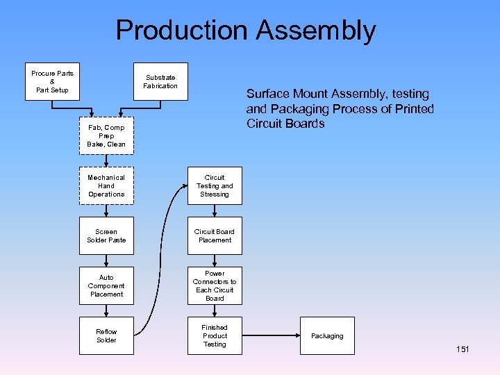
Production Assembly Procure Parts & Part Setup Substrate Fabrication Surface Mount Assembly, testing and Packaging Process of Printed Circuit Boards Fab, Comp Prep Bake, Clean Mechanical Hand Operations Circuit Testing and Stressing Screen Solder Paste Circuit Board Placement Auto Component Placement Power Connectors to Each Circuit Board Reflow Solder Finished Product Testing Packaging 151
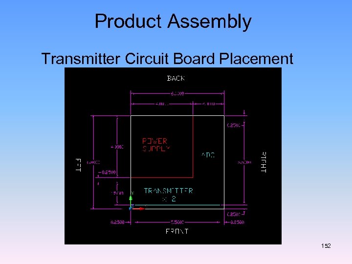
Product Assembly Transmitter Circuit Board Placement 152
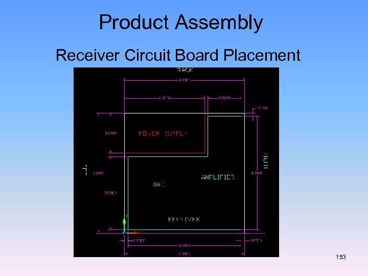
Product Assembly Receiver Circuit Board Placement 153
Mass Production Assembly • Circuit Testing – Power Supplies • With-in nominal range of specified output voltages – Audio Amplifier (8Ω Load) • Frequency Response • Gain • SNR & THD 154
Mass Production Assembly • Finished Product Testing – Meets Transmit and Receive Distances – SNR & THD – ESD • Stressing – Thermal Cycling – Mechanical Shock and Vibration – EMC 155

Capstone Design Team #2 Acknowledgements • Special Thanks to – Harley-Davidson Motor Company – Jim Cummins – Rajendra Naik – Jeff Kautzer 156
Prototype Demonstration 157
7d1218c5aee8ba78723232769abc91ef.ppt