

финмен слай АЗ.pptx
- Количество слайдов: 6
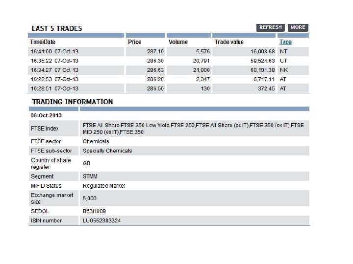
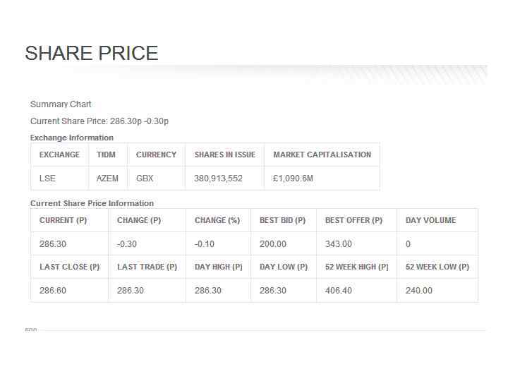
 HISTORY AZ is") AZEM AZ ELECTRONIC MATERIALS S. A. ORD USD 0. 10 (DI) HISTORY AZ is a leading global producer and supplier of high quality, high-purity specialty chemical materials, operating in the high growth electronics market. Its materials are widely used in integrated circuits (“ICs”) and devices, flat panel displays (“FPDs”), lightemitting diodes (“LEDs”) and photolithographic printing. AZ is a critical partner to the leading global electronic players because our chemical technology allows them to enhance existing processes and enables them to innovate new products. This is critically important in the “digital world” where there is increasing global demand a drive towards smaller, faster, more powerful and less expensive technology. AZ operates in 10 countries, namely China, India, South Korea, Taiwan, Hong Kong, Japan, Singapore, the USA, France and Germany. It also has corporate and support services offices in Luxembourg, the UK and Hong Kong, and employs over 1, 000 people globally. The AZ business was originally a part of Hoechst AG, the former German chemicals company. The name AZ (pronounced “A-Zee”) is taken from the photoreactive group name diazo, first developed around 1943 and used around 1950 to create photosensitive offset printing plates, and later adapted for use in ICs and FPDs. Ever since, AZ has been at the forefront of photoresist technology, selling the first broadband series photoresists under the AZ® trademark in 1962 and becoming the first supplier of photoresists to the FPD industry in the 1980’s. AZ’s international expansion and sustained investment in R&D, together with its unique relationship with its customers, are amongst the key factors that have driven the business’ success. The time chart below highlights some key milestones in AZ’s journey to date.
AZEM AZ ELECTRONIC MATERIALS S. A. ORD USD 0. 10 (DI) HISTORY AZ is a leading global producer and supplier of high quality, high-purity specialty chemical materials, operating in the high growth electronics market. Its materials are widely used in integrated circuits (“ICs”) and devices, flat panel displays (“FPDs”), lightemitting diodes (“LEDs”) and photolithographic printing. AZ is a critical partner to the leading global electronic players because our chemical technology allows them to enhance existing processes and enables them to innovate new products. This is critically important in the “digital world” where there is increasing global demand a drive towards smaller, faster, more powerful and less expensive technology. AZ operates in 10 countries, namely China, India, South Korea, Taiwan, Hong Kong, Japan, Singapore, the USA, France and Germany. It also has corporate and support services offices in Luxembourg, the UK and Hong Kong, and employs over 1, 000 people globally. The AZ business was originally a part of Hoechst AG, the former German chemicals company. The name AZ (pronounced “A-Zee”) is taken from the photoreactive group name diazo, first developed around 1943 and used around 1950 to create photosensitive offset printing plates, and later adapted for use in ICs and FPDs. Ever since, AZ has been at the forefront of photoresist technology, selling the first broadband series photoresists under the AZ® trademark in 1962 and becoming the first supplier of photoresists to the FPD industry in the 1980’s. AZ’s international expansion and sustained investment in R&D, together with its unique relationship with its customers, are amongst the key factors that have driven the business’ success. The time chart below highlights some key milestones in AZ’s journey to date.
 • • • • • AZ History 1957: Develops first positive photoresists for use in the manufacture of ICs 1967: Establishes presence in Taiwan through toll manufacturing of photoresists 1971: Opens new manufacturing facility in the USA 1986: Opens new manufacturing facility in Japan, supplying photoresist to the FPD industry 1989: Starts production of FPD materials in South Korea 1997: Taiwanese operation begins supply of EBR through a toll manufacturing arrangement 1997: Clariant AG, a Swiss chemicals company, acquires Hoechst AG’s specialty chemicals operations, including the AZ business 1998: Opens new manufacturing facility and functional testing centre in South Korea 1999: Opens new manufacturing facility and functional testing centre in the USA 2003: First commercial sales of dielectrics and pattern enhancement products, both used in the manufacturing of ICs 2004: AZ acquired by The Carlyle Group and established as a standalone business for the first time. 2004: Opens new manufacturing facility in Taiwan 2005: Opens new manufacturing facility in China 2007: Vestar Capital Partners invests in AZ 2008: Invests in new dielectrics and FPD photoresist production facilities in Japan and Taiwan respectively 2009: Moves large portion of FPD photoresist production from Japan to Taiwan 2010: Admitted to trading on the London Stock Exchange’s main market and included in the FTSE 250 index 2011: Acquires polysilazanes coatings and resins business from Clariant AG, including the world’s only commercial organic polysilazane manufacturing plant, located in India 2012: Opens new manufacturing facility in Taiwan
 • • Further miniaturisation, in line with Moore’s Law, will require further advancements in specialty chemicals. Semiconductors are created in patterned layers, which ultimately form a complete integrated circuit. As the number of layers on a semiconductor rises, so can the demand for the latest advanced chemicals. Products such as anti-reflective coatings to improve pattern uniformity and fidelity, specialty rinses to reduce pattern collapse and defects, and chemical shrink materials for controlled reduction of feature sizes, are essential for enabling die size reductions and enhancing manufacturing yields. One new material innovation is negative-tone development (“NTD”), in which the light-sensitive material used to create patterns on the semiconductor (known as the photoresist) is exposed to light and the organic solvent used for development removes the unexposed material, effectively reversing the imaging. This provides finer resolution capabilities and process window performance. The use of NTD in manufacturing is aided by new anti-collapse rinse agents to gain the process window improvements needed to deliver cost-of-ownership benefits. Chemical shrink materials are also finding use in NTD flows to further push resolution, enabling even finer feature patterning with installed lithographic tool sets. With smaller and smaller patterns needed, new patterning techniques such as extreme ultra-violet (“EUV”) lithography and directed self-assembly (“DSA”) are likely to be required. EUV will require the use of new coating and protection materials, while DSA – which may offer a very significant reduction in cost-of-ownership compared with EUV – requires entirely new materials which are being pioneered by AZ. Memory chips continue to advance. Smaller feature sizes are being developed allowing higher capacity in a smaller space, as well as lower energy use. 3 D NAND (a type of flash memory) is being developed for the future, where memory cells will be stacked on top of each other. New chemical materials products and processes will be needed for these memory chips, again driving demand for companies such as AZ.