4f9c836e45b492183aa09fc005d5dcb3.ppt
- Количество слайдов: 39
 Automatic Test Generation and Logic Optimization
 Types of Errors in a Digital System • Software error : detected by design validation – Design (conceptual) faults – Implementation faults • Hardware error : detected by testing – Physical faults
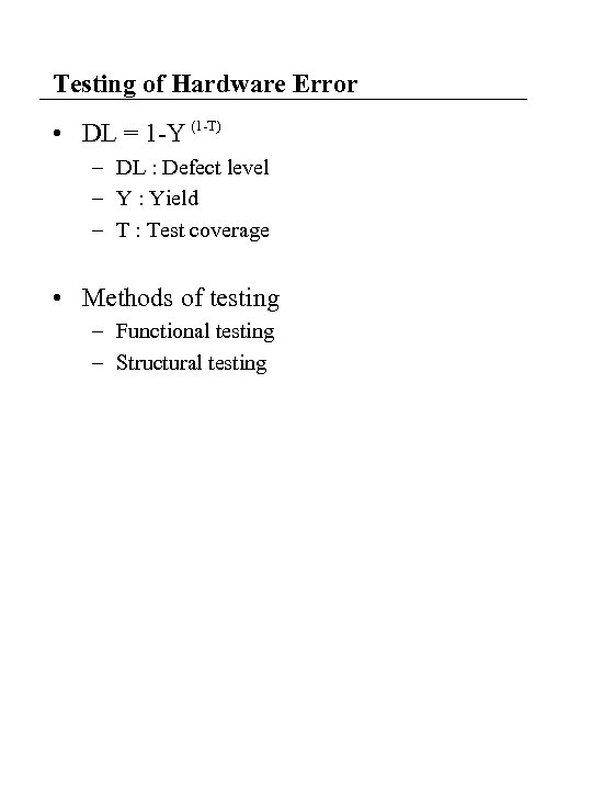 Testing of Hardware Error • DL = 1 -Y (1 -T) – DL : Defect level – Y : Yield – T : Test coverage • Methods of testing – Functional testing – Structural testing
 Faults and Fault Models • Fault – shorts, defective soldering, … • Fault model – stuck-at fault – bridging fault – stuck-open fault • Single stuck-at-0/1 fault – computationally efficient – represents most of defects which occur in real logic devices – detects many faults of other types
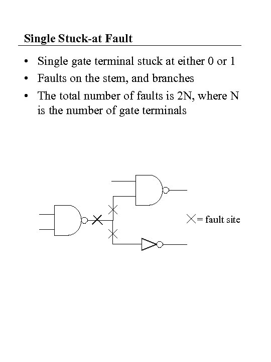 Single Stuck-at Fault • Single gate terminal stuck at either 0 or 1 • Faults on the stem, and branches • The total number of faults is 2 N, where N is the number of gate terminals = fault site
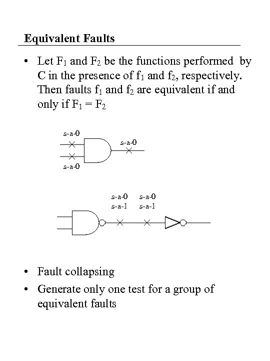 Equivalent Faults • Let F 1 and F 2 be the functions performed by C in the presence of f 1 and f 2, respectively. Then faults f 1 and f 2 are equivalent if and only if F 1 = F 2 s-a-0 s-a-1 s-a-0 s-a-1 • Fault collapsing • Generate only one test for a group of equivalent faults
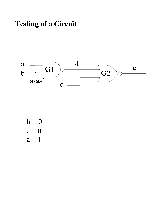 Testing of a Circuit a b G 1 s-a-1 c b=0 c=0 a=1 d G 2 e
 Controlling and Non-controlling Value • Controlling value : when it present on at least one input of a gate, it forces the output to a known value – AND gate, NAND gate : 0 – OR gate, NOR gate : 1 • Non-controlling value : the complement of (Sensitizing value) the controlling value – AND gate, NAND gate : 1 – OR gate, NOR gate : 0
 Automatic Test Generation • Three steps – Set up (fault sensitizing) – Propagation (path sensitizing) – Justification (consistency check)
 Test Generation (D-Algorithm) • The setup step is to produce a difference in the output signal at the gate where the fault is located between the two cases when the fault is present or it is absent stuck-at 1 H s-a-1 0 1 D= H D 0 when fault occurs 1 no fault D is called frontier
 Test Generation (D-Algorithm) • The propagation step derives the D (or D) condition from the faulty gate to a output stuck-at 1 0 1 1 H D J D
 Test Generation (D-Algorithm) • The last step is to force the logic values needed to sensitize the assumed fault from the primary inputs A B 1 1 F 0 s-a-1 H C D 0 X E 1 G 1 J D
 Backtracking a b G 2 c e G 1 s-a-1 G 4 d G 3 g f 1. excitation condition a = b = 1 2. sensitization condition f = 0 3. choose d = 1 b = 0 (conflict) try c = 1 (succeed) • Backtracking : returning on one’s step and reversing a previous choice
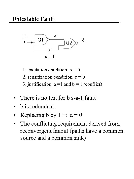 Untestable Fault a b G 1 c G 2 d s-a-1 1. excitation condition b = 0 2. sensitization condition c = 0 3. justification a =1 and b = 1 (conflict) • • There is no test for b s-a-1 fault b is redundant Replacing b by 1 d = 0 The conflicting requirement derived from reconvergent fanout (paths have a common source and a common sink)
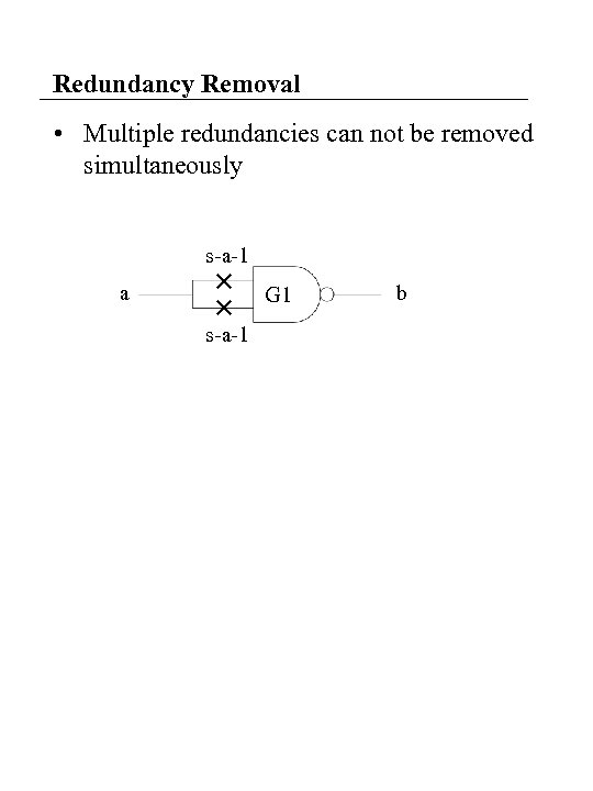 Redundancy Removal • Multiple redundancies can not be removed simultaneously s-a-1 a G 1 s-a-1 b
 Redundancy Removal • The result of redundancy removal depends on the order in which redundancies are removed a b c d G 2 s-a-0 G 1 e G 4 g f G 3 Initial Circuit a b c d G 1 s-a-1 G 2 G 3 G 4 e g f After the removal of s-a-0 redundancy a c G 1 b G 3 d f G 4 After the removal of the remaining redundancy g
 Desirable Property of Redundancy Removal • Increase the testability • Reduce area • Improve the performance by reducing the capacitive loads and the number of series transistors
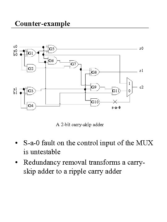 Counter-example c 0 a 0 b 0 G 1 G 6 G 2 a 1 b 1 G 3 G 4 s 0 G 5 G 7 s 1 G 8 G 9 1 G 11 0 c 2 G 10 s-a-0 A 2 -bit carry-skip adder • S-a-0 fault on the control input of the MUX is untestable • Redundancy removal transforms a carryskip adder to a ripple carry adder
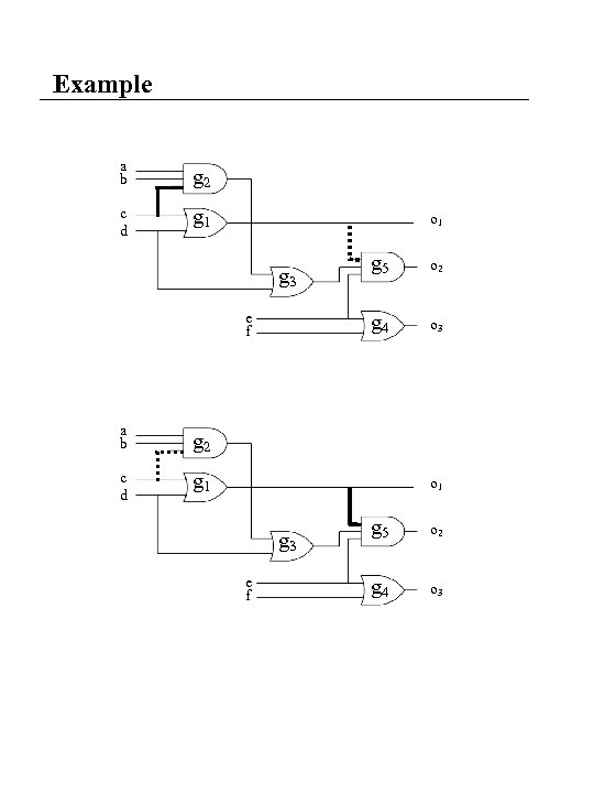
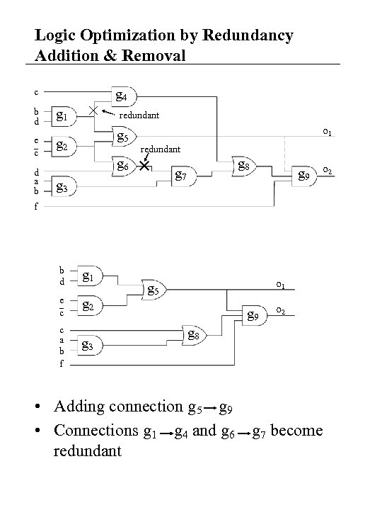 Logic Optimization by Redundancy Addition & Removal c b d e c d a b g 4 g 1 redundant g 5 g 2 o 1 redundant g 6 g 8 g 7 g 3 g 9 o 2 f b d g 1 e c g 2 c a b f g 3 o 1 g 5 g 9 o 2 g 8 • Adding connection g 5 g 9 • Connections g 1 g 4 and g 6 g 7 become redundant
 Definition c b d e c d a b g 4 g 1 g 2 g 6 g 3 o 1 g 5 g 7 g 8 g 9 o 2 f • Absolute dominator (dominator) of a wire W: the set of gates G such that all paths from wire W to any primary output have to pass through all gates in G • Ex : dominators of g 1 g 4 : g 4, g 8, g 9
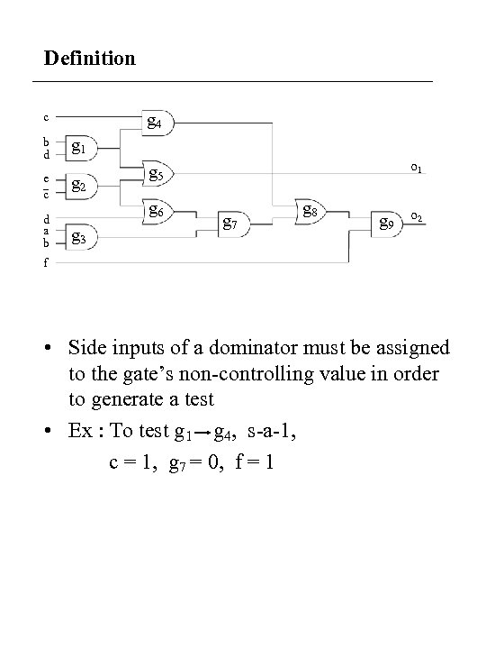 Definition c b d e c d a b g 4 g 1 g 2 g 6 g 3 o 1 g 5 g 7 g 8 g 9 o 2 f • Side inputs of a dominator must be assigned to the gate’s non-controlling value in order to generate a test • Ex : To test g 1 g 4, s-a-1, c = 1, g 7 = 0, f = 1
 Mandatory Assignments • The value assignments required for a test to exist and they must be satisfied by any test vector • Use implication to compute MA • To compute entire set of MA is NP-complete • Derive SMA (Set of Mandatory Assignment) from dominators
 Single Alternative Wire • Step 1 : Calculate Mandatory Assignment for target faults • Step 2 : Identify a set of candidate connections to be added. Each addition will make the target fault untestable (redundant) • Step 3 : Check whether a candidate is redundant • Step 1 and Step 3 can be performed by implication and checking of the consistency of the SMA
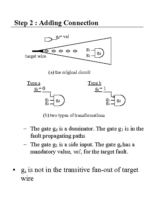 Step 2 : Adding Connection gs= val g 1 g 2 target wire gd (a) the original circuit Type a gs = 0 Type b gs = 1 g 2 gd g 1 g 2 gd (b) two types of transformations – The gate gd is a dominator. The gate g 1 is in the fault propagating paths – The gate g 2 is a side input. The gate gs has a mandatory value, val, for the target fault. • gs is not in the transitive fan-out of target wire
 Example a b g 2 c d g 1 o 1 e f a b o 2 o 3 g 2 c d g 5 g 4 g 3 g 1 o 1 g 3 e f g 5 o 2 g 4 o 3
 False Path Identification
 Static Delay Analysis 1 1 3 3 c g 2 d e h f • arrival time : from input to output • required time : from output to input • slack = required time - arrival time
 Timing Analysis Problems • We want to determine the true critical paths of a circuit in order to: – To determine the minimum cycle time that the circuit will function – To identify critical paths for performance optimization – don’t want to try to optimize the wrong (non-critical) paths • Implications: – Don’t want false paths (produced by static delay analysis)
 False Paths • Static analysis is fast but leads to false paths • Path of length 400 is never “exercised” u x fj 200 100 v 1 MUX 0 fi 200 100 y 1 MUX 0 s • Approaches: 1. Mark orthogonal pairs – May be wrong, can’t find all possibilities 2. Throw out non-sensitizable (false) paths • Circuit delay = Length of longest path ? – Not a good enough bound (too pessimistic) • Circuit delay = Time of last output change => Functional timing analysis for false paths
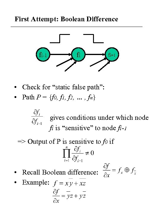 First Attempt: Boolean Difference fi-1 fi fi+1 • Check for “static false path”: • Path P = {f 0, f 1, f 2, … , fn} gives conditions under which node fi is “sensitive” to node fi-1 => Output of P is sensitive to f 0 if • Recall Boolean difference: • Example:
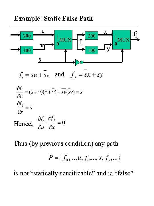 Example: Static False Path 200 100 u v 1 MUX 0 fi 200 100 x y 1 MUX 0 s and Hence, Thus (by previous condition) any path is not “statically sensitizable” and is “false” fj
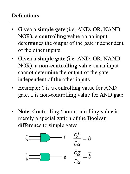 Definitions • Given a simple gate (i. e. AND, OR, NAND, NOR), a controlling value on an input determines the output of the gate independent of the other inputs • Given a simple gate (i. e. AND, OR, NAND, NOR), a non-controlling value on an input cannot determine the output of the gate independent of the other inputs • Example: 0 is a controlling value for AND gate. 1 is non-controlling value for AND gate • Note: Controlling / non-controlling value is merely a specialization of the Boolean difference to simple gates a b f a b g
 Static Sensitization • Simple Gates: Let path P = {f 0, f 1, …, fi} • A side-input to a gate fi along P is any input other than fi-1 • An event is a transition from 0 to 1 or 1 to 0 • Path P is statically sensitizable if there exists a primary input vector under which every side-input is set to a non-controlling value • A path is a “statically false path” if it is not statically sensitizable (see previous example)
 Static Sensitization and False Paths • Static sensitization is wrong! a b d 1 1 e 1 c f 1 g a b c constant 0 d e f g t= 0 1 2 3 • Paths shown in bold are not statically sensitizable, but delay of circuit is 3
 Why Static Sensitization Fails • Static sensitization fails because it considers only the final value on each side-input. It does not consider values on side-inputs at the moment the event propagates from fi-1 through node fi • For example, in previous circuit when determining static sensitization of path {b, e, f, g} we assume side-input a of gate e is at final non-controlling value of 1. This is not necessary for the path to be sensitizable
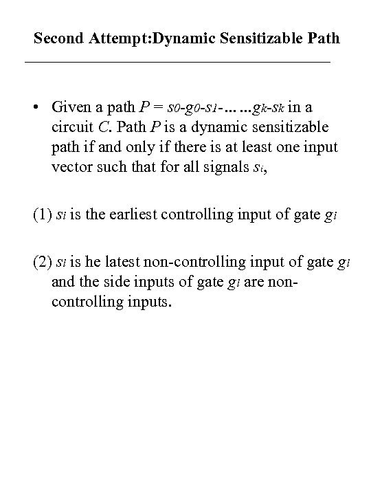 Second Attempt: Dynamic Sensitizable Path • Given a path P = s 0 -g 0 -s 1 -……gk-sk in a circuit C. Path P is a dynamic sensitizable path if and only if there is at least one input vector such that for all signals si, (1) si is the earliest controlling input of gate gi (2) si is he latest non-controlling input of gate gi and the side inputs of gate gi are noncontrolling inputs.
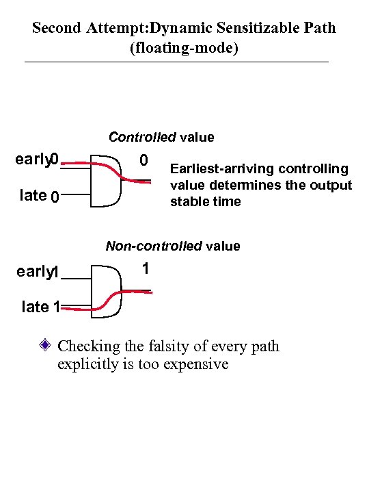 Second Attempt: Dynamic Sensitizable Path (floating-mode) Controlled value early 0 0 late 0 Earliest-arriving controlling value determines the output stable time Non-controlled value early 1 1 late 1 Checking the falsity of every path explicitly is too expensive
 False Path Analysis • State-of-the-art approach: – D = topological longest path delay – Is there an input vector under which an output gets stable only after or at t =D? (*) • No: Decrease D and try it again • Yes: The delay is D. Done • (*) is a SAT problem
 Algorithm Early-arrive-signals (si, *) = {sj | sj is an input signal to gate gi and Max-arrive-time(sj) < Min. PD(si, P, *)} Late-arrrive-signals (si, *) = {sj | sj is an input signal to gate gi and Min-arrive-time (sj) > Max. PD (si, P, *)} Algorithm false_path_checking (P, false_path) let P be the path to be checked and P=s 0, g 0, s 1, g 1, …, si, gi, …, sk where s 0 and sk are a primary input and a primary output respectively let Q be the event Queue and the format of event is (si, val), where val is the logic value assigned to signal si begin {The event generating phase} Initialize Q for each si alogn the path P do begin for each sj Early-arrive-signals(si, *) do begin enqueue(sj, val = non-control value of gate gi) into Q end if Late-arrive-signals(si, *) then begin enqueue(si, val=control value of gate gi) into Q end


