683ab4d2583d091fe16a5ba208d51f53.ppt
- Количество слайдов: 74
Array Structured Memories STMicro/Intel UCSD CAD LAB Weste Text EE 141 STMicro/Intel/UCSD/THNU 1 Memory
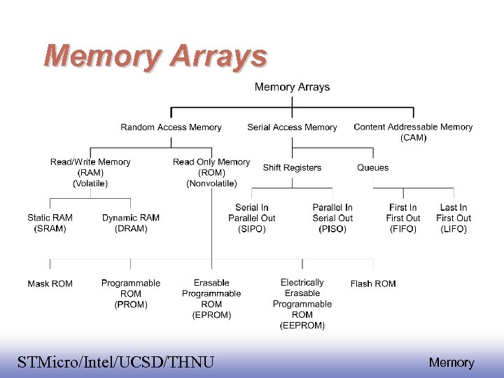
Memory Arrays EE 141 STMicro/Intel/UCSD/THNU 2 Memory
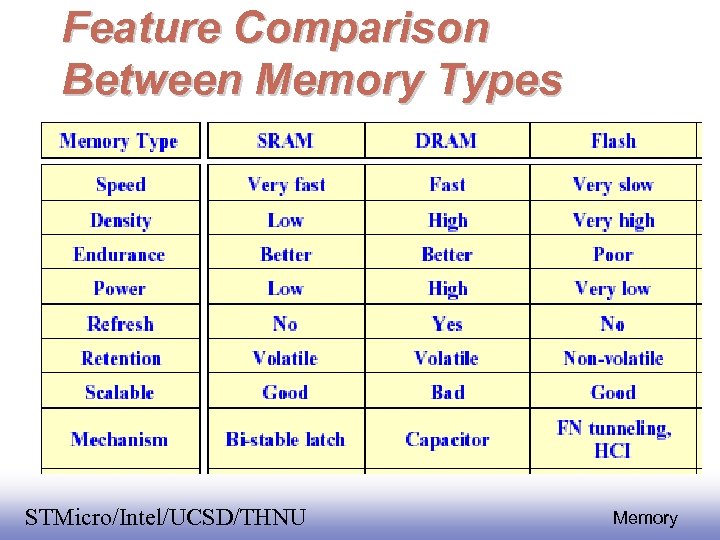
Feature Comparison Between Memory Types EE 141 STMicro/Intel/UCSD/THNU 3 Memory
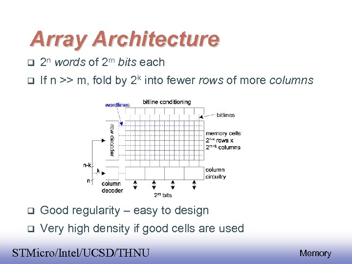
Array Architecture 2 n words of 2 m bits each If n >> m, fold by 2 k into fewer rows of more columns Good regularity – easy to design Very high density if good cells are used EE 141 STMicro/Intel/UCSD/THNU 4 Memory
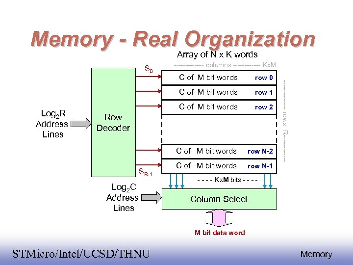
Memory - Real Organization Array of N x K words S 0 ------- columns ------ Kx. M row 1 C of M bit words row 2 C of M bit words row N-1 Row Decoder SR-1 Log 2 C Address Lines ------- rows R------ row 0 C of M bit words Log 2 R Address Lines C of M bit words - - Kx. M bits - - Column Select M bit data word EE 141 STMicro/Intel/UCSD/THNU 5 Memory
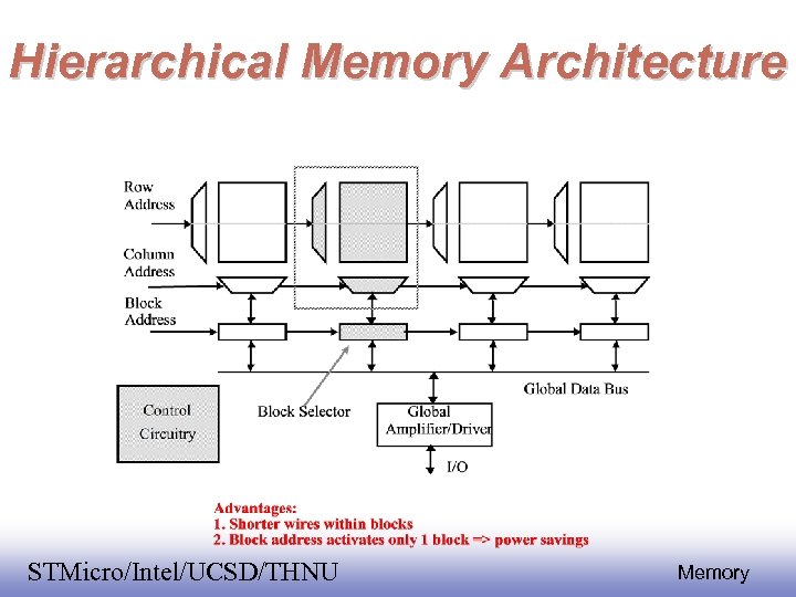
Hierarchical Memory Architecture EE 141 STMicro/Intel/UCSD/THNU 6 Memory
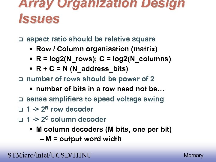
Array Organization Design Issues aspect ratio should be relative square Row / Column organisation (matrix) R = log 2(N_rows); C = log 2(N_columns) R + C = N (N_address_bits) number of rows should be power of 2 number of bits in a row need not be… sense amplifiers to speed voltage swing 1 -> 2 R row decoder 1 -> 2 C column decoder M column decoders (M bits, one per bit) – M = output word width EE 141 STMicro/Intel/UCSD/THNU 7 Memory
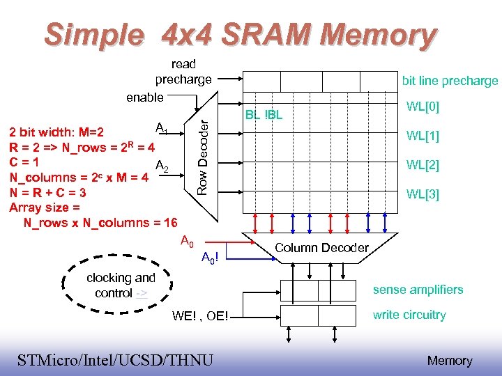
Simple 4 x 4 SRAM Memory Row Decoder read precharge enable A 1 2 bit width: M=2 R = 2 => N_rows = 2 R = 4 C=1 A 2 c x M = 4 N_columns = 2 N=R+C=3 Array size = N_rows x N_columns = 16 A 0! clocking and control -> bit line precharge BL !BL WL[0] WL[1] WL[2] WL[3] Column Decoder sense amplifiers WE! , OE! EE 141 STMicro/Intel/UCSD/THNU write circuitry 8 Memory
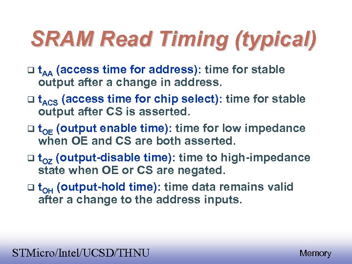
SRAM Read Timing (typical) t. AA (access time for address): time for stable output after a change in address. t. ACS (access time for chip select): time for stable output after CS is asserted. t. OE (output enable time): time for low impedance when OE and CS are both asserted. t. OZ (output-disable time): time to high-impedance state when OE or CS are negated. t. OH (output-hold time): time data remains valid after a change to the address inputs. EE 141 STMicro/Intel/UCSD/THNU 9 Memory
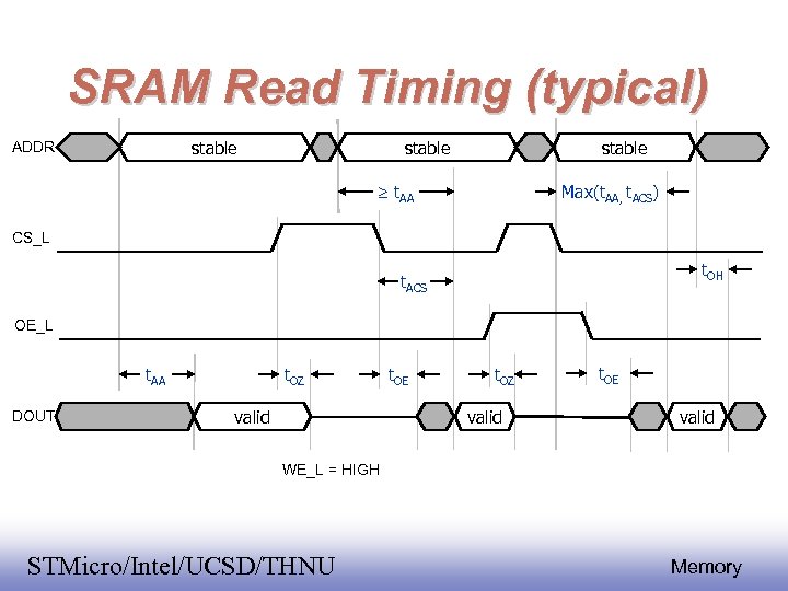
SRAM Read Timing (typical) stable ADDR stable t. AA Max(t. AA, t. ACS) CS_L t. OH t. ACS OE_L t. AA DOUT t. OZ t. OE t. OZ valid t. OE valid WE_L = HIGH EE 141 STMicro/Intel/UCSD/THNU 10 Memory
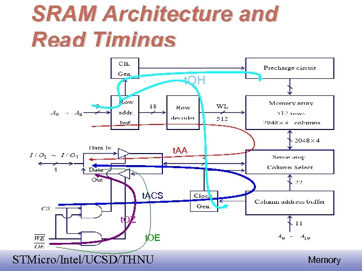
SRAM Architecture and Read Timings t. OH t. AA t. ACS t. OZ t. OE EE 141 STMicro/Intel/UCSD/THNU 11 Memory
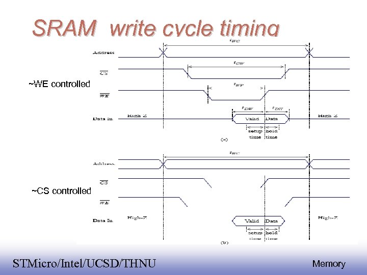
SRAM write cycle timing ~WE controlled ~CS controlled EE 141 STMicro/Intel/UCSD/THNU 12 Memory
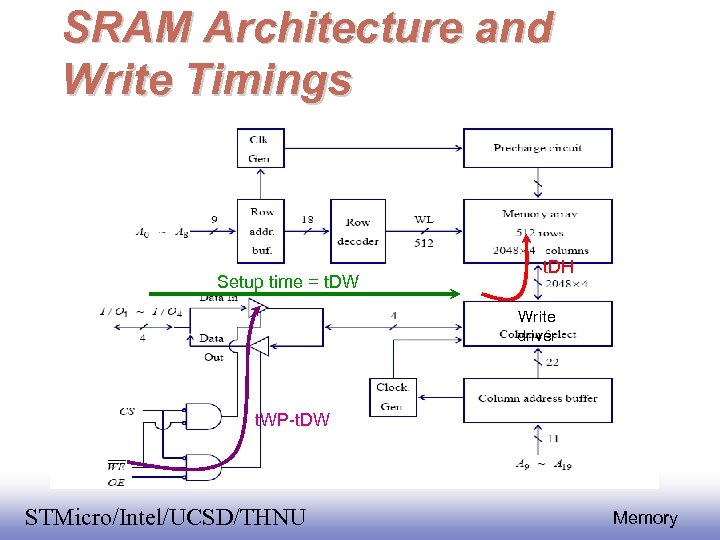
SRAM Architecture and Write Timings Setup time = t. DW t. DH Write driver t. WP-t. DW EE 141 STMicro/Intel/UCSD/THNU 13 Memory
SRAM Cell Design Memory arrays are large Need to optimize cell design for area and performance Peripheral circuits can be complex – 60 -80% area in array, 20 -40% in periphery Classical Memory cell design 6 T cell full CMOS 4 T cell with high resistance poly load TFT load cell EE 141 STMicro/Intel/UCSD/THNU 14 Memory
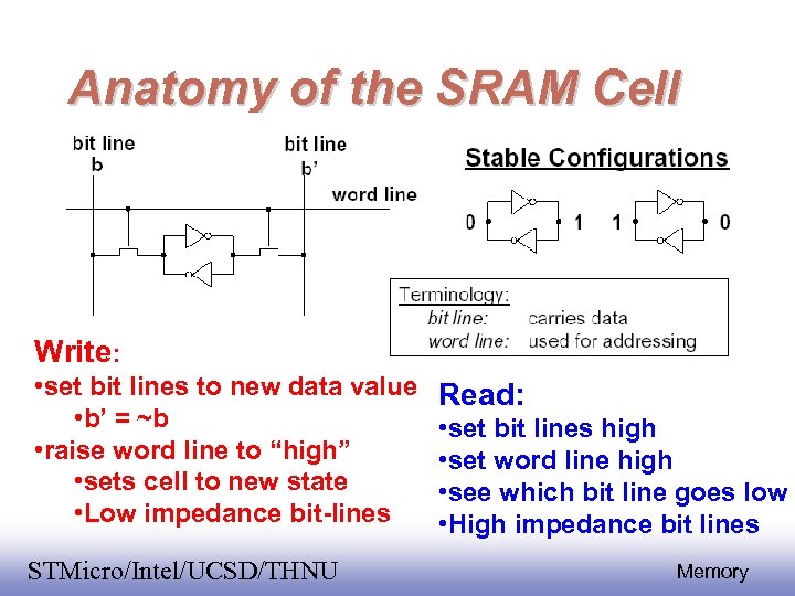
Anatomy of the SRAM Cell Write: • set bit lines to new data value • b’ = ~b • raise word line to “high” • sets cell to new state • Low impedance bit-lines EE 141 STMicro/Intel/UCSD/THNU Read: • set bit lines high • set word line high • see which bit line goes low • High impedance bit lines 15 Memory
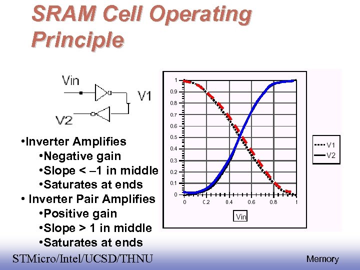
SRAM Cell Operating Principle • Inverter Amplifies • Negative gain • Slope < – 1 in middle • Saturates at ends • Inverter Pair Amplifies • Positive gain • Slope > 1 in middle • Saturates at ends EE 141 STMicro/Intel/UCSD/THNU 16 Memory
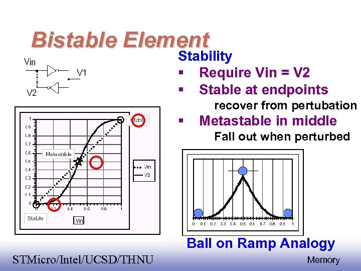
Bistable Element Stability Require Vin = V 2 Stable at endpoints recover from pertubation Metastable in middle Fall out when perturbed Ball on Ramp Analogy EE 141 STMicro/Intel/UCSD/THNU 17 Memory
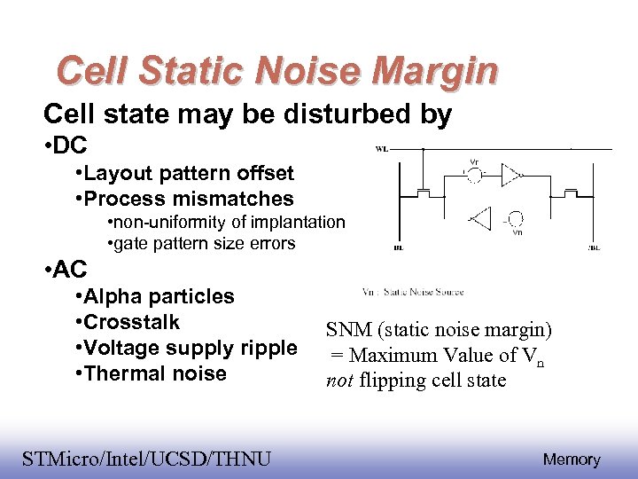
Cell Static Noise Margin Cell state may be disturbed by • DC • Layout pattern offset • Process mismatches • non-uniformity of implantation • gate pattern size errors • AC • Alpha particles • Crosstalk • Voltage supply ripple • Thermal noise EE 141 STMicro/Intel/UCSD/THNU SNM (static noise margin) = Maximum Value of Vn not flipping cell state 18 Memory
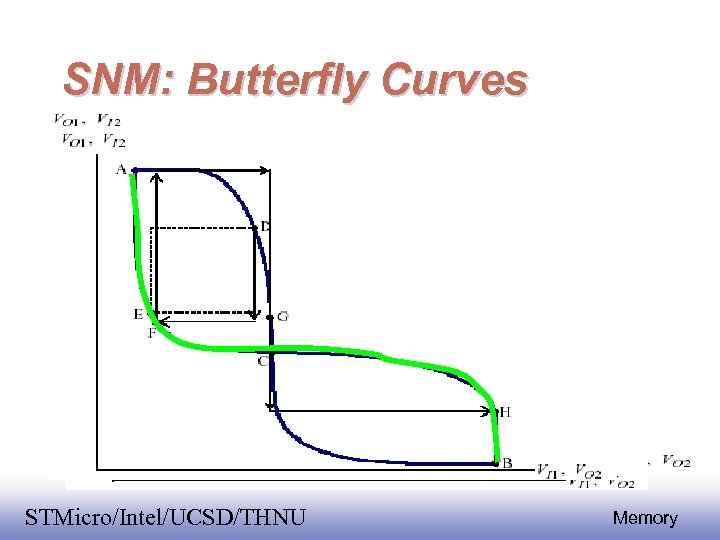
SNM: Butterfly Curves 1 SNM 2 2 SNM 1 2 1 EE 141 STMicro/Intel/UCSD/THNU 1 2 19 Memory
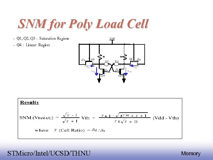
SNM for Poly Load Cell EE 141 STMicro/Intel/UCSD/THNU 20 Memory
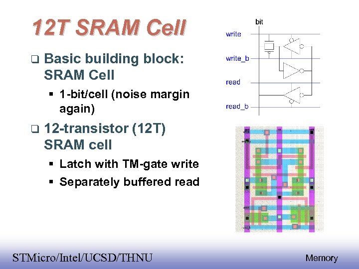
12 T SRAM Cell Basic building block: SRAM Cell 1 -bit/cell (noise margin again) 12 -transistor (12 T) SRAM cell Latch with TM-gate write Separately buffered read EE 141 STMicro/Intel/UCSD/THNU 21 Memory
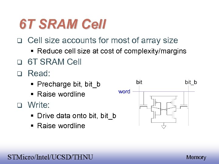
6 T SRAM Cell size accounts for most of array size Reduce cell size at cost of complexity/margins 6 T SRAM Cell Read: Precharge bit, bit_b Raise wordline Write: Drive data onto bit, bit_b Raise wordline EE 141 STMicro/Intel/UCSD/THNU 22 Memory
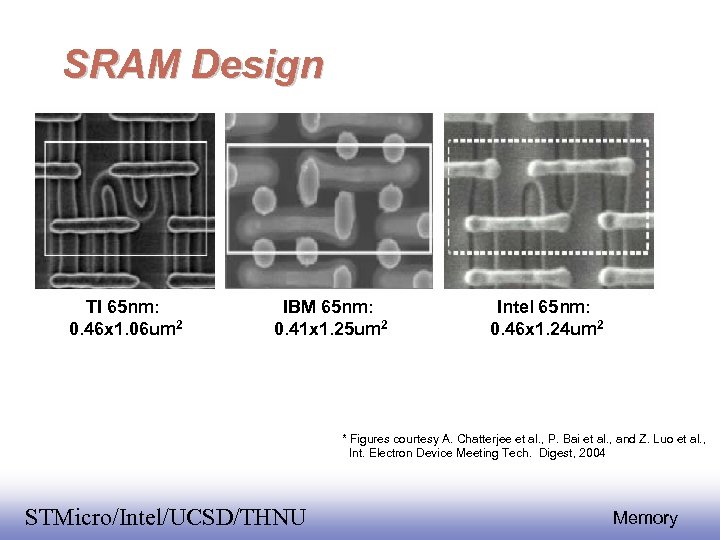
SRAM Design TI 65 nm: 0. 46 x 1. 06 um 2 IBM 65 nm: 0. 41 x 1. 25 um 2 Intel 65 nm: 0. 46 x 1. 24 um 2 * Figures courtesy A. Chatterjee et al. , P. Bai et al. , and Z. Luo et al. , Int. Electron Device Meeting Tech. Digest, 2004 EE 141 STMicro/Intel/UCSD/THNU 23 Memory
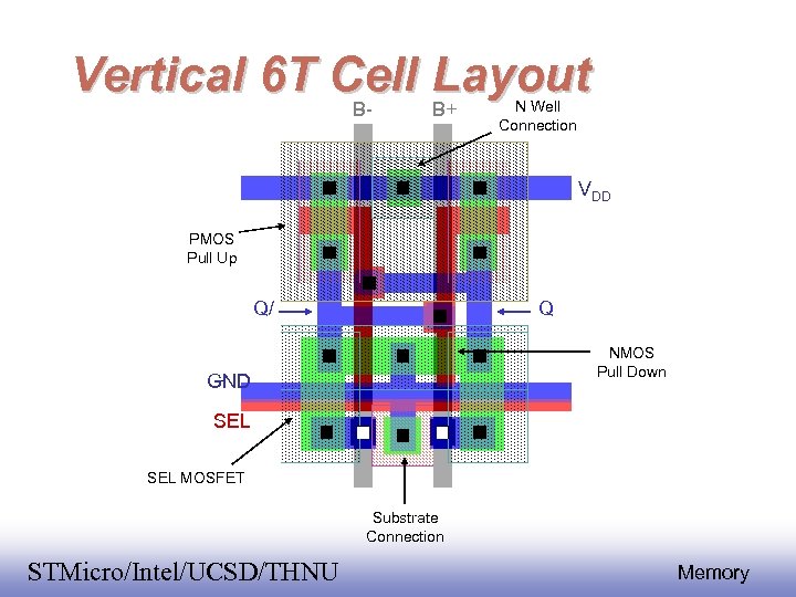
Vertical 6 T Cell Layout BB+ N Well Connection VDD PMOS Pull Up Q/ Q NMOS Pull Down GND SEL MOSFET Substrate Connection EE 141 STMicro/Intel/UCSD/THNU 24 Memory
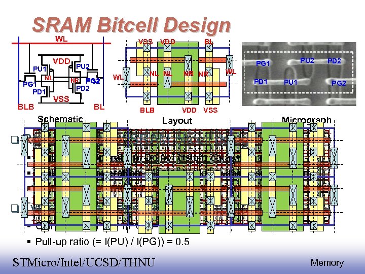
SRAM Bitcell Design WL PU 1 VDD NL PG 1 PD 1 BLB VSS PU 2 PG 2 PD 2 NR VSS BL Schematic Requirements WL VDD NL NL BLB BL NR NR WL PU 2 PG 1 PD 2 PU 1 PG 2 VDD VSS Layout Micrograph of SRAM bitcell design Stable read operation: Do not disturb data when reading Stable write operation: Must write data within a specified time Stable data retention: Data should not be lost Typical transistor sizing Cell ratio (= I(PD) / I(PG)) = 1. 5 ~ 2. 5 Pull-up ratio (= I(PU) / I(PG)) = 0. 5 EE 141 STMicro/Intel/UCSD/THNU 25 Memory
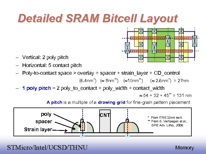
Detailed SRAM Bitcell Layout – Vertical: 2 poly pitch – Horizontal: 5 contact pitch – Poly-to-contact space > overlay + spacer + strain_layer + CD_control (6. 4 nm *) ( 8 nm**) ( 10 nm**) ( 2. 6 nm*) = 27 nm – 1 poly pitch = 2 poly_to_contact + poly_width + contact_width 54 + 32 + 45** = 131 nm A pitch is a multiple of a drawing grid for fine-grain pattern placement Ex. : 5 grid per pitch drawing grid = (131/5) = 26 nm poly CNT * From ITRS 22 tech. Ex. : 6 grid per pitch drawing grid = (131/6) = 32 nm nmal. , ** From S. Verhaegen et spacer Strain layer EE 141 STMicro/Intel/UCSD/THNU SPIE Adv. Litho. , 2008 26 Memory
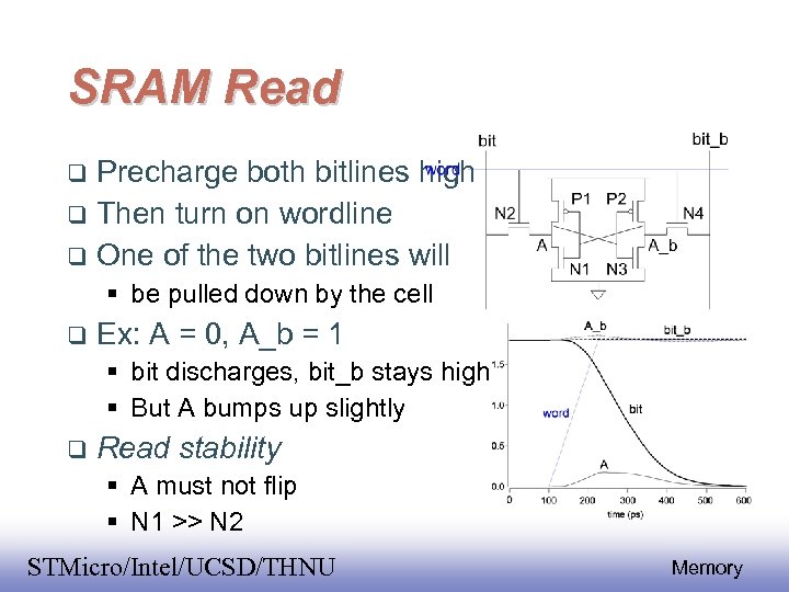
SRAM Read Precharge both bitlines high Then turn on wordline One of the two bitlines will be pulled down by the cell Ex: A = 0, A_b = 1 bit discharges, bit_b stays high But A bumps up slightly Read stability A must not flip N 1 >> N 2 EE 141 STMicro/Intel/UCSD/THNU 27 Memory
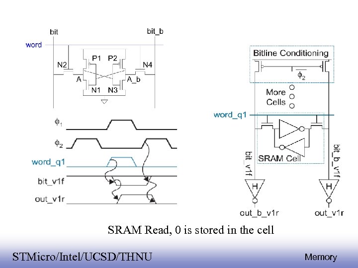
SRAM Read, 0 is stored in the cell EE 141 STMicro/Intel/UCSD/THNU 28 Memory
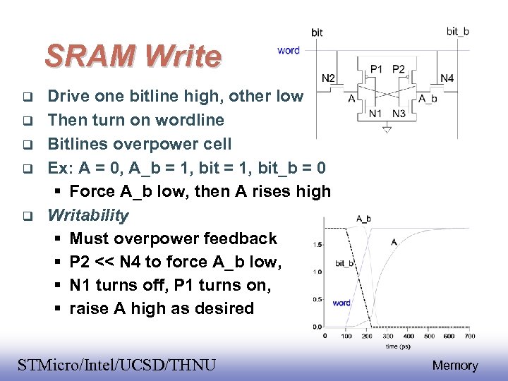
SRAM Write Drive one bitline high, other low Then turn on wordline Bitlines overpower cell Ex: A = 0, A_b = 1, bit_b = 0 Force A_b low, then A rises high Writability Must overpower feedback P 2 << N 4 to force A_b low, N 1 turns off, P 1 turns on, raise A high as desired EE 141 STMicro/Intel/UCSD/THNU 29 Memory
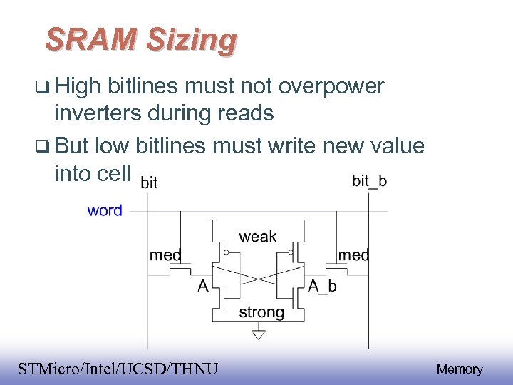
SRAM Sizing High bitlines must not overpower inverters during reads But low bitlines must write new value into cell EE 141 STMicro/Intel/UCSD/THNU 30 Memory
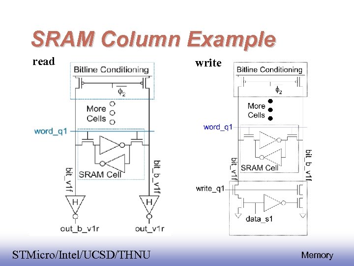
SRAM Column Example read EE 141 STMicro/Intel/UCSD/THNU write 31 Memory
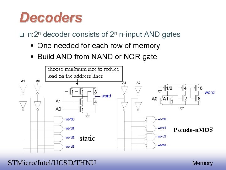
Decoders n: 2 n decoder consists of 2 n n-input AND gates One needed for each row of memory Build AND from NAND or NOR gate choose minimum size to reduce load on the address lines Pseudo-n. MOS static EE 141 STMicro/Intel/UCSD/THNU 32 Memory
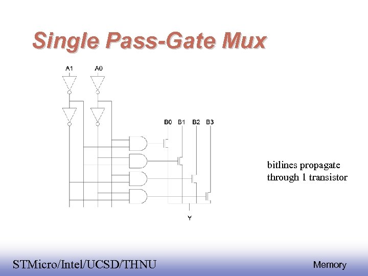
Single Pass-Gate Mux bitlines propagate through 1 transistor EE 141 STMicro/Intel/UCSD/THNU 33 Memory
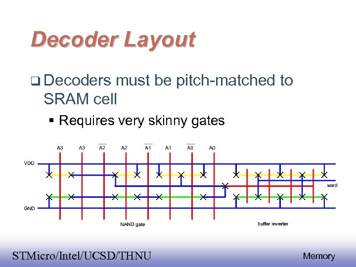
Decoder Layout Decoders must be pitch-matched to SRAM cell Requires very skinny gates EE 141 STMicro/Intel/UCSD/THNU 34 Memory
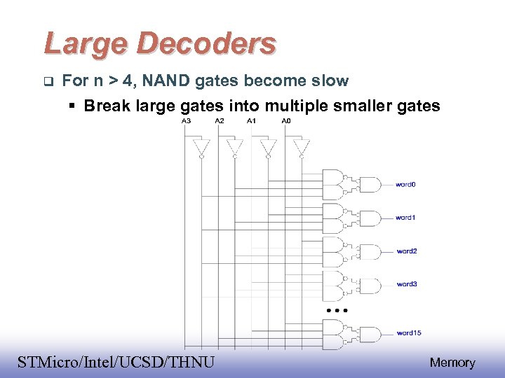
Large Decoders For n > 4, NAND gates become slow Break large gates into multiple smaller gates EE 141 STMicro/Intel/UCSD/THNU 35 Memory
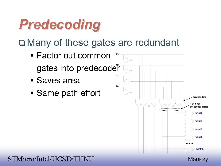
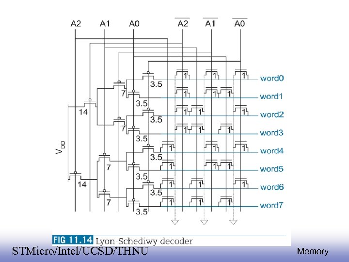
Predecoding Many of these gates are redundant Factor out common gates into predecoder Saves area Same path effort EE 141 STMicro/Intel/UCSD/THNU 36 Memory
EE 141 STMicro/Intel/UCSD/THNU 37 Memory
Column Circuitry Some circuitry is required for each column Bitline conditioning Sense amplifiers Column multiplexing Each column must have write drivers and read sensing circuits EE 141 STMicro/Intel/UCSD/THNU 38 Memory
Column Multiplexing Recall that array may be folded for good aspect ratio Ex: 2 k word x 16 folded into 256 rows x 128 columns Must select 16 output bits from the 128 columns Requires 16 8: 1 column multiplexers EE 141 STMicro/Intel/UCSD/THNU 39 Memory
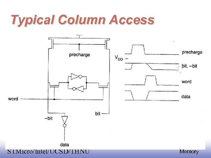
Typical Column Access EE 141 STMicro/Intel/UCSD/THNU 40 Memory
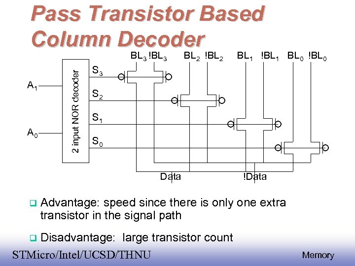
Pass Transistor Based Column Decoder A 1 A 0 2 input NOR decoder BL 3 !BL 3 BL 2 !BL 2 S 3 S 2 S 1 S 0 Data BL 1 !BL 1 BL 0 !Data Advantage: speed since there is only one extra transistor in the signal path Disadvantage: large transistor count EE 141 STMicro/Intel/UCSD/THNU 41 Memory
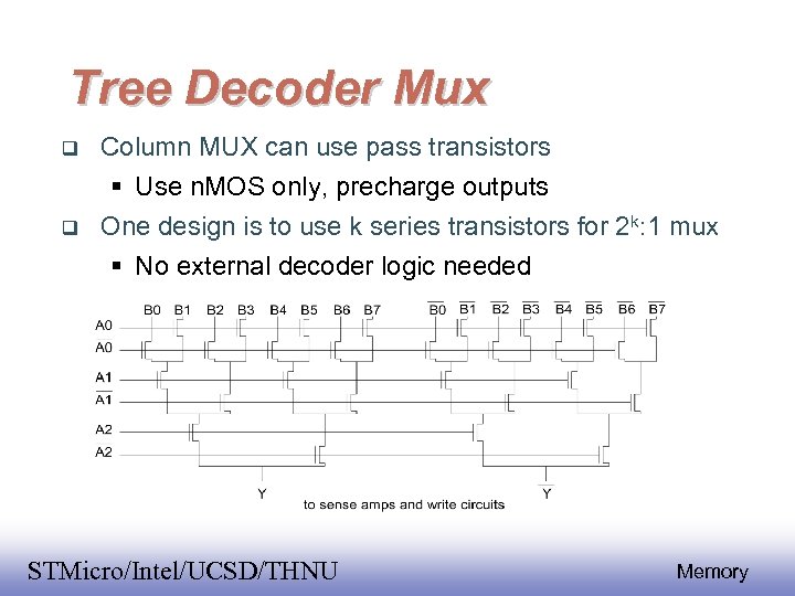
Tree Decoder Mux Column MUX can use pass transistors Use n. MOS only, precharge outputs One design is to use k series transistors for 2 k: 1 mux No external decoder logic needed EE 141 STMicro/Intel/UCSD/THNU 42 Memory
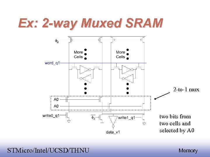
Ex: 2 -way Muxed SRAM 2 -to-1 mux two bits from two cells and selected by A 0 EE 141 STMicro/Intel/UCSD/THNU 43 Memory
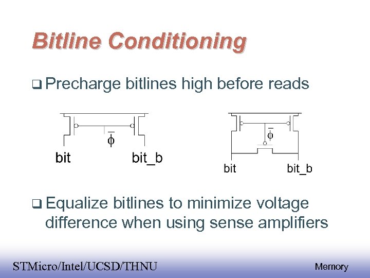
Bitline Conditioning Precharge bitlines high before reads Equalize bitlines to minimize voltage difference when using sense amplifiers EE 141 STMicro/Intel/UCSD/THNU 44 Memory
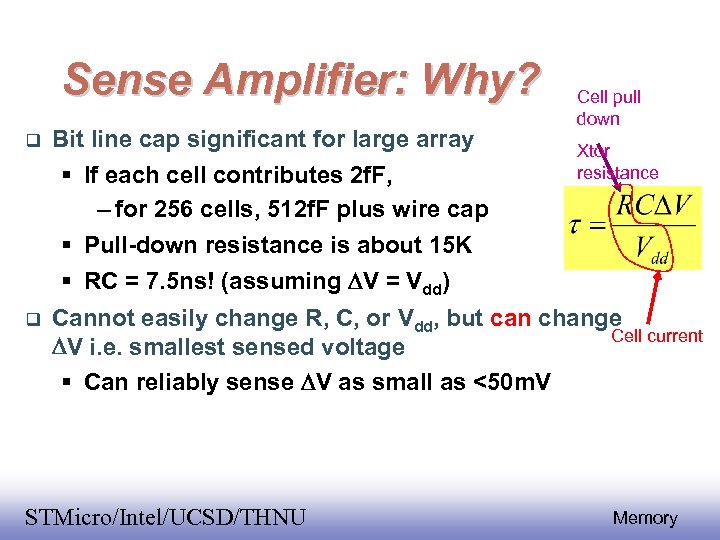
Sense Amplifier: Why? Cell pull down Bit line cap significant for large array If each cell contributes 2 f. F, – for 256 cells, 512 f. F plus wire cap Pull-down resistance is about 15 K RC = 7. 5 ns! (assuming DV = Vdd) Cannot easily change R, C, or Vdd, but can change Cell current DV i. e. smallest sensed voltage Can reliably sense DV as small as <50 m. V EE 141 STMicro/Intel/UCSD/THNU Xtor resistance 45 Memory
Sense Amplifiers Bitlines have many cells attached Ex: 32 -kbit SRAM has 256 rows x 128 cols 128 cells on each bitline tpd (C/I) DV Even with shared diffusion contacts, 64 C of diffusion capacitance (big C) Discharged slowly through small transistors (small I) Sense amplifiers are triggered on small voltage swing (reduce DV) EE 141 STMicro/Intel/UCSD/THNU 46 Memory
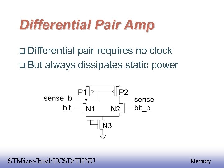
Differential Pair Amp Differential pair requires no clock But always dissipates static power EE 141 STMicro/Intel/UCSD/THNU 47 Memory
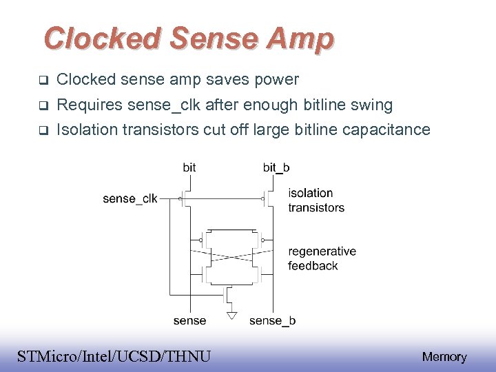
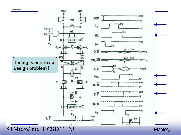
Clocked Sense Amp Clocked sense amp saves power Requires sense_clk after enough bitline swing Isolation transistors cut off large bitline capacitance EE 141 STMicro/Intel/UCSD/THNU 48 Memory
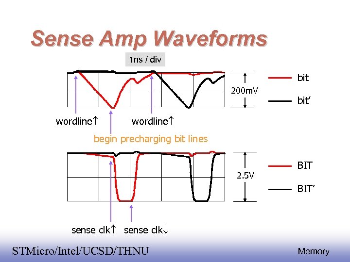
Sense Amp Waveforms 1 ns / div bit 200 m. V wordline bit’ wordline begin precharging bit lines 2. 5 V BIT’ sense clk EE 141 STMicro/Intel/UCSD/THNU 49 Memory
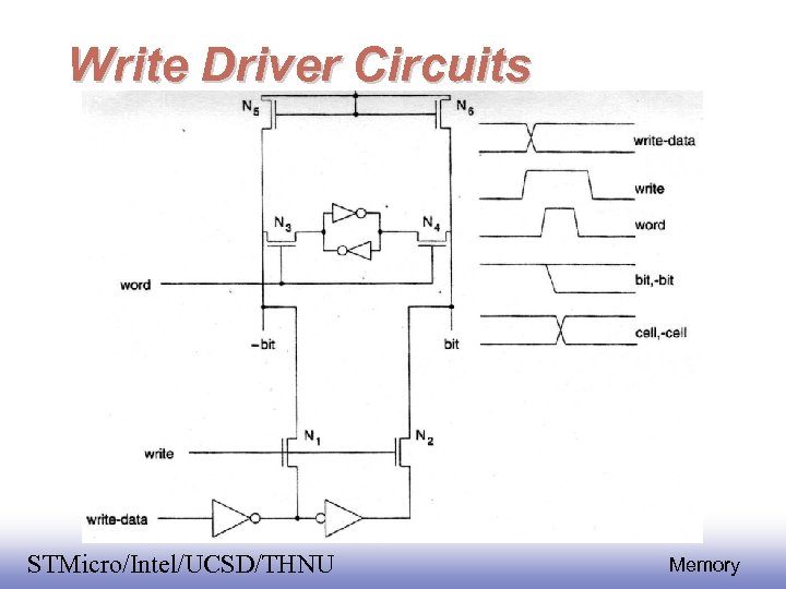
Write Driver Circuits EE 141 STMicro/Intel/UCSD/THNU 50 Memory
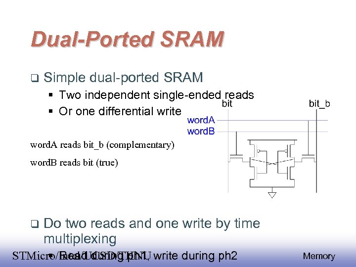
Dual-Ported SRAM Simple dual-ported SRAM Two independent single-ended reads Or one differential write word. A reads bit_b (complementary) word. B reads bit (true) Do two reads and one write by time multiplexing EE 141 STMicro/Intel/UCSD/THNU write during ph 2 Read during ph 1, 51 Memory
Multiple Ports We have considered single-ported SRAM One read or one write on each cycle Multiported SRAM are needed for register files Examples: Multicycle MIPS must read two sources or write a result on some cycles Pipelined MIPS must read two sources and write a third result each cycle Superscalar MIPS must read and write many sources and results each cycle EE 141 STMicro/Intel/UCSD/THNU 52 Memory
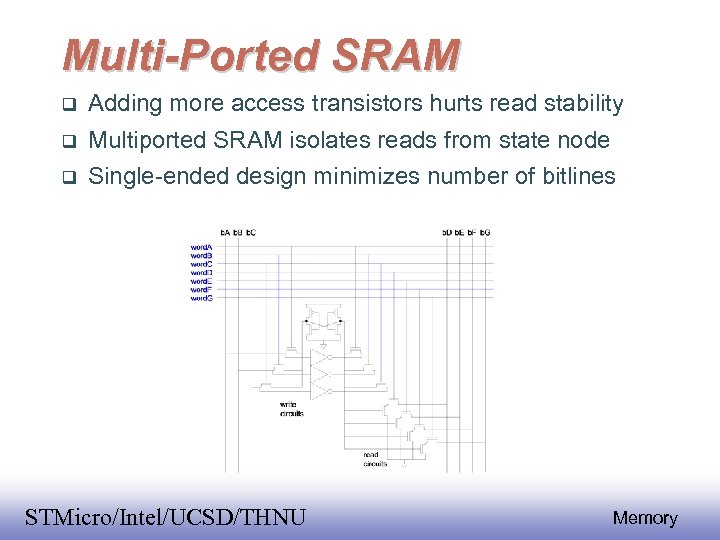
Multi-Ported SRAM Adding more access transistors hurts read stability Multiported SRAM isolates reads from state node Single-ended design minimizes number of bitlines EE 141 STMicro/Intel/UCSD/THNU 53 Memory
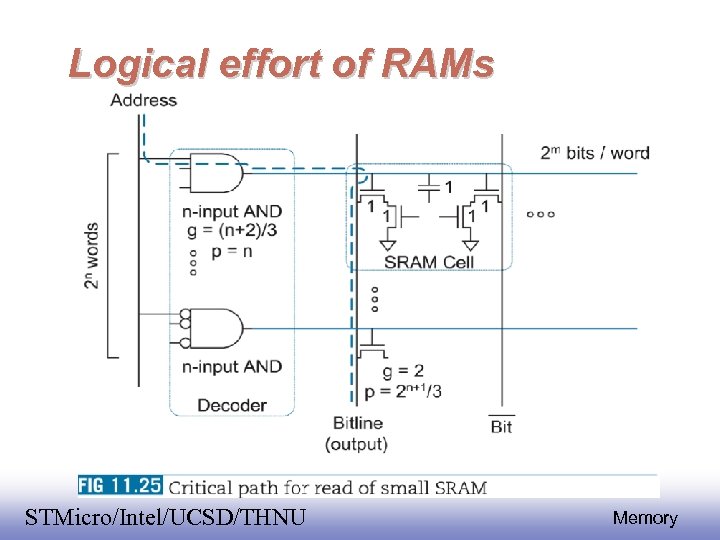
Logical effort of RAMs EE 141 STMicro/Intel/UCSD/THNU 54 Memory
EE 141 STMicro/Intel/UCSD/THNU 55 Memory
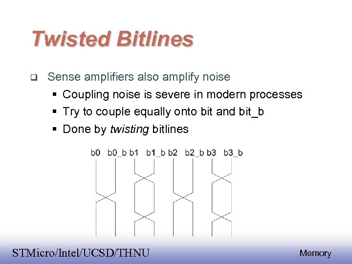
Twisted Bitlines Sense amplifiers also amplify noise Coupling noise is severe in modern processes Try to couple equally onto bit and bit_b Done by twisting bitlines EE 141 STMicro/Intel/UCSD/THNU 56 Memory
Alternative SRAM Cells Low Voltage/High Leakage/Process Variations crowd the operating margins of conventional SRAM Alternative Sense Amplifiers, column and row arrangements, adaptive timing, smaller hierarchy, redundant and spare rows/columns have all been addressed in the literature with some success. Some problems come from the cell design itself– modifying the cell can break conflicting demands for optimization EE 141 STMicro/Intel/UCSD/THNU 57 Memory
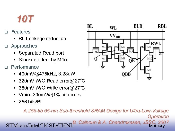
10 T Features BL Leakage reduction Approaches Separated Read port Stacked effect by M 10 Performance 400 m. V@475 k. Hz, 3. 28 u. W 320 m. V W/O Read error@27℃ 380 m. V W/O Write error@27℃ Vmin=300 m. V@1% bit errors 256 bits/BL A 256 -kb 65 -nm Sub-threshold SRAM Design for Ultra-Low-Voltage Operation B. Calhoun & A. Chandrakasan, JSSC, 58 2007 EE 141 STMicro/Intel/UCSD/THNU Memory
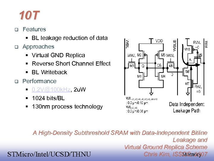
10 T Features BL leakage reduction of data Approaches Virtual GND Replica Reverse Short Channel Effect BL Writeback Performance 0. 2 V@100 k. Hz, 2 u. W 1024 bits/BL 130 nm process technology A High-Density Subthreshold SRAM with Data-Independent Bitline Leakage and Virtual Ground Replica Scheme 59 Chris Kim, ISSCC, 2007 Memory EE 141 STMicro/Intel/UCSD/THNU
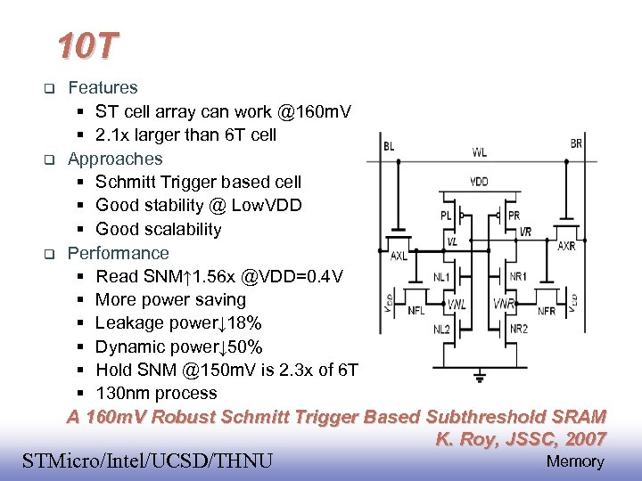
10 T Features ST cell array can work @160 m. V 2. 1 x larger than 6 T cell Approaches Schmitt Trigger based cell Good stability @ Low. VDD Good scalability Performance Read SNM↑ 1. 56 x @VDD=0. 4 V More power saving Leakage power↓ 18% Dynamic power↓ 50% Hold SNM @150 m. V is 2. 3 x of 6 T 130 nm process A 160 m. V Robust Schmitt Trigger Based Subthreshold SRAM K. Roy, JSSC, 2007 60 EE 141 STMicro/Intel/UCSD/THNU Memory
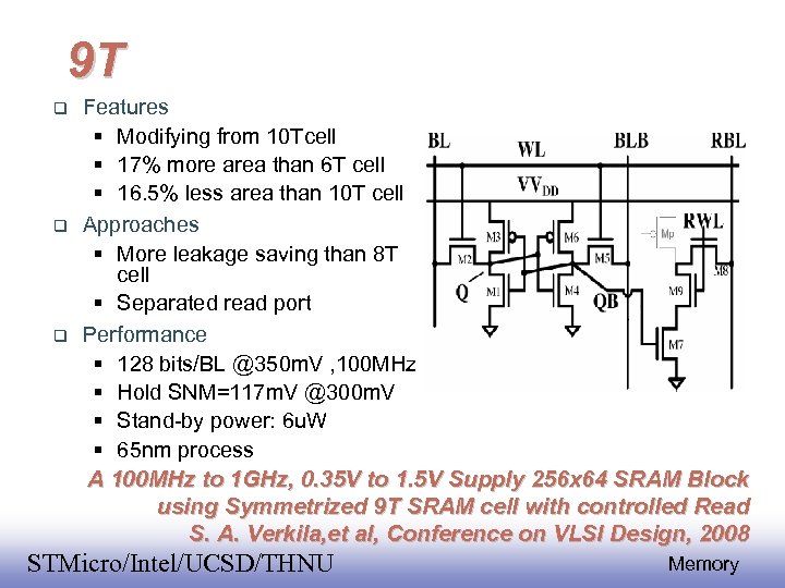
9 T Features Modifying from 10 Tcell 17% more area than 6 T cell 16. 5% less area than 10 T cell Approaches More leakage saving than 8 T cell Separated read port Performance 128 bits/BL @350 m. V , 100 MHz Hold SNM=117 m. V @300 m. V Stand-by power: 6 u. W 65 nm process A 100 MHz to 1 GHz, 0. 35 V to 1. 5 V Supply 256 x 64 SRAM Block using Symmetrized 9 T SRAM cell with controlled Read S. A. Verkila, et al, Conference on VLSI Design, 2008 EE 141 STMicro/Intel/UCSD/THNU 61 Memory
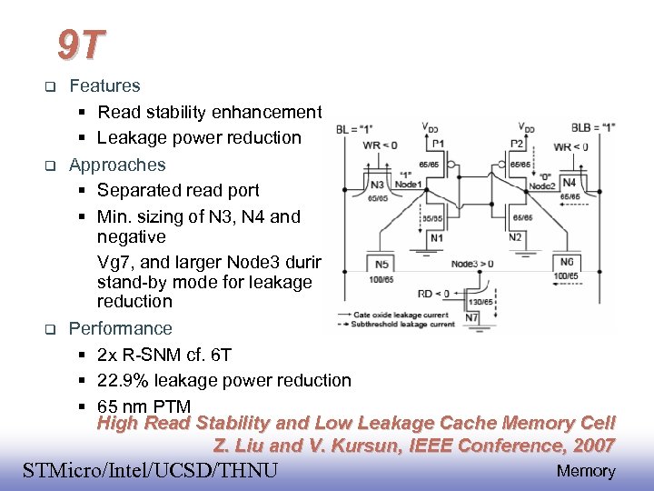
9 T Features Read stability enhancement Leakage power reduction Approaches Separated read port Min. sizing of N 3, N 4 and negative Vg 7, and larger Node 3 during stand-by mode for leakage reduction Performance 2 x R-SNM cf. 6 T 22. 9% leakage power reduction 65 nm PTM High Read Stability and Low Leakage Cache Memory Cell Z. Liu and V. Kursun, IEEE Conference, 2007 EE 141 STMicro/Intel/UCSD/THNU 62 Memory
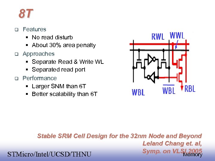
8 T Features No read disturb About 30% area penalty Approaches Separate Read & Write WL Separated read port Performance Larger SNM than 6 T Better scalability than 6 T Stable SRM Cell Design for the 32 nm Node and Beyond Leland Chang et. al, 63 Symp. on VLSI, 2005 Memory EE 141 STMicro/Intel/UCSD/THNU
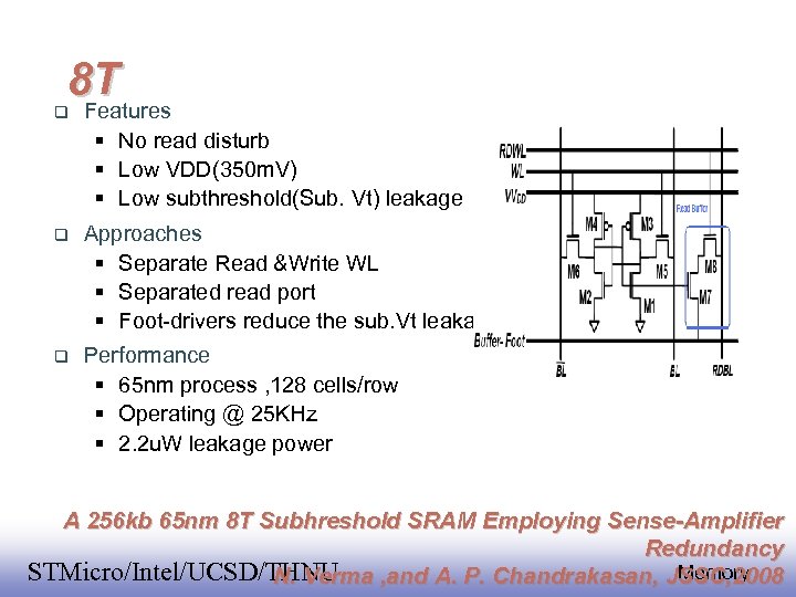
8 T Features No read disturb Low VDD(350 m. V) Low subthreshold(Sub. Vt) leakage Approaches Separate Read &Write WL Separated read port Foot-drivers reduce the sub. Vt leakage Performance 65 nm process , 128 cells/row Operating @ 25 KHz 2. 2 u. W leakage power A 256 kb 65 nm 8 T Subhreshold SRAM Employing Sense-Amplifier Redundancy 64 Memory EE 141 STMicro/Intel/UCSD/THNU N. Verma , and A. P. Chandrakasan, JSSC, 2008
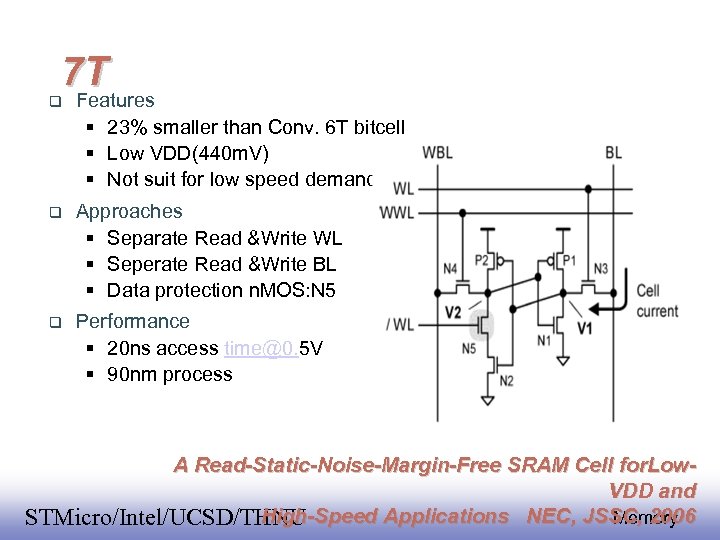
7 T Features 23% smaller than Conv. 6 T bitcell Low VDD(440 m. V) Not suit for low speed demand Approaches Separate Read &Write WL Seperate Read &Write BL Data protection n. MOS: N 5 Performance 20 ns access time@0. 5 V 90 nm process A Read-Static-Noise-Margin-Free SRAM Cell for. Low. VDD and 65 High-Speed Applications NEC, JSSC, 2006 Memory EE 141 STMicro/Intel/UCSD/THNU
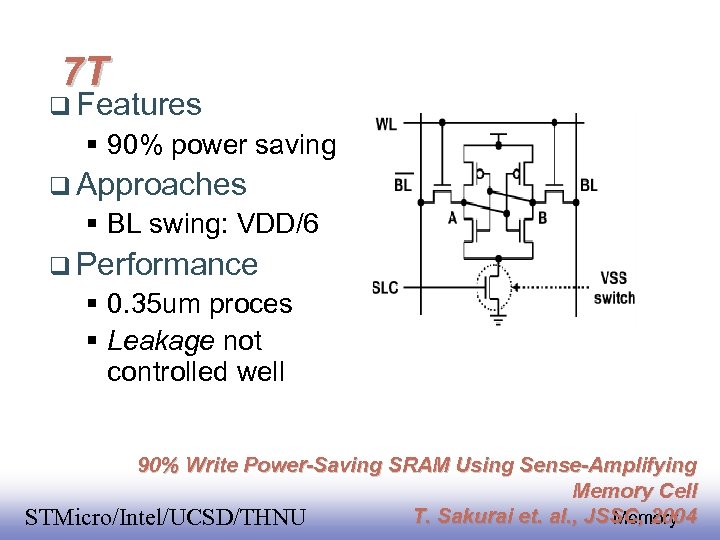
7 T Features 90% power saving Approaches BL swing: VDD/6 Performance 0. 35 um proces Leakage not controlled well 90% Write Power-Saving SRAM Using Sense-Amplifying Memory Cell 66 T. Sakurai et. al. , JSSC, 2004 Memory EE 141 STMicro/Intel/UCSD/THNU
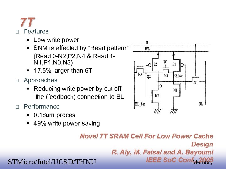
7 T Features Low write power SNM is effected by “Read pattern” (Read 0 -N 2, P 2, N 4 & Read 1 N 1, P 1, N 3, N 5) 17. 5% larger than 6 T Approaches Reducing write power by cut off the (feedback) connection to BL Performance 0. 18 um proces 49% write power saving Novel 7 T SRAM Cell For Low Power Cache Design R. Aly, M. Faisal and A. Bayoumi 67 IEEE So. C Conf. , 2005 Memory EE 141 STMicro/Intel/UCSD/THNU
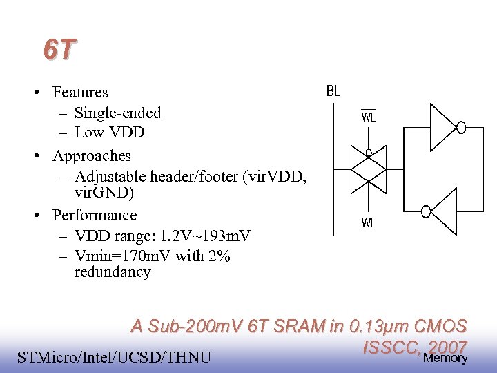
6 T • Features – Single-ended – Low VDD • Approaches – Adjustable header/footer (vir. VDD, vir. GND) • Performance – VDD range: 1. 2 V~193 m. V – Vmin=170 m. V with 2% redundancy A Sub-200 m. V 6 T SRAM in 0. 13μm CMOS 68 ISSCC, Memory 2007 EE 141 STMicro/Intel/UCSD/THNU
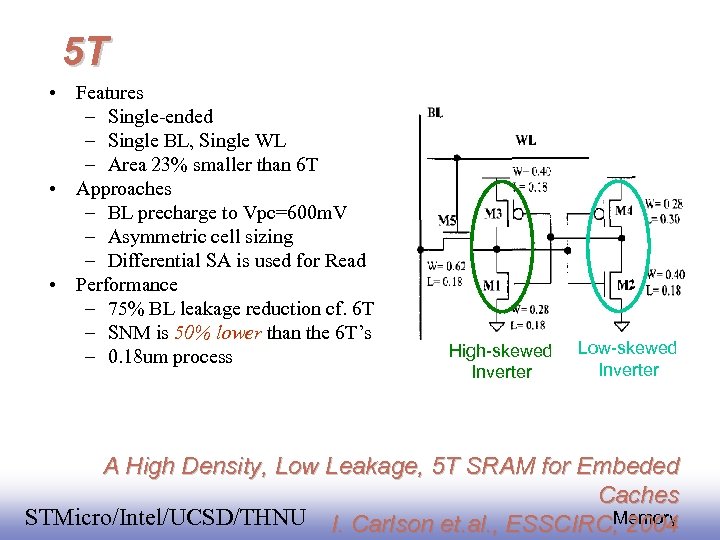
5 T • Features – Single-ended – Single BL, Single WL – Area 23% smaller than 6 T • Approaches – BL precharge to Vpc=600 m. V – Asymmetric cell sizing – Differential SA is used for Read • Performance – 75% BL leakage reduction cf. 6 T – SNM is 50% lower than the 6 T’s – 0. 18 um process High-skewed Inverter Low-skewed Inverter A High Density, Low Leakage, 5 T SRAM for Embeded Caches 69 Memory EE 141 STMicro/Intel/UCSD/THNU I. Carlson et. al. , ESSCIRC, 2004
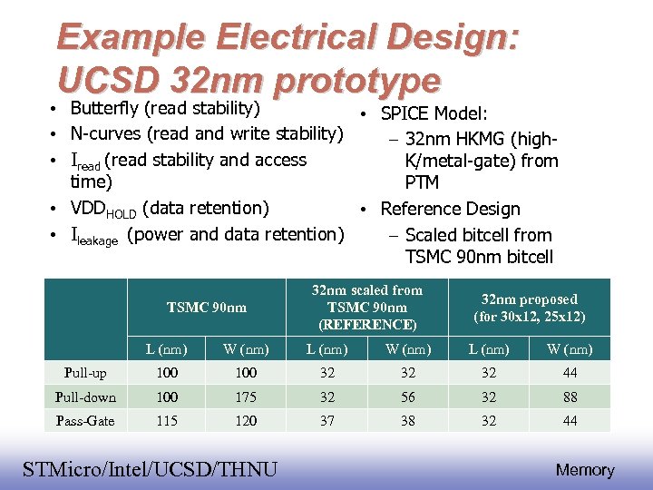
Example Electrical Design: UCSD 32 nm prototype • Butterfly (read stability) • SPICE Model: • N-curves (read and write stability) – 32 nm HKMG (high • Iread (read stability and access K/metal-gate) from time) PTM • VDDHOLD (data retention) • Reference Design • Ileakage (power and data retention) – Scaled bitcell from TSMC 90 nm bitcell TSMC 90 nm 32 nm scaled from TSMC 90 nm (REFERENCE) 32 nm proposed (for 30 x 12, 25 x 12) L (nm) W (nm) Pull-up 100 32 32 32 44 Pull-down 100 175 32 56 32 88 Pass-Gate 115 120 37 38 32 44 EE 141 STMicro/Intel/UCSD/THNU 70 Memory
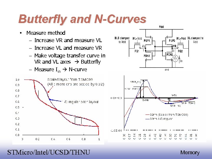
Butterfly and N-Curves • Measure method – Increase VR and measure VL – Increase VL and measure VR – Make voltage transfer curve in VR and VL axes Butterfly – Measure Iin N-curve EE 141 STMicro/Intel/UCSD/THNU 71 Memory
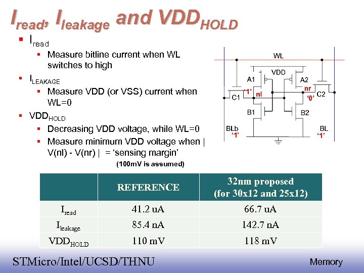
Iread, Ileakage and VDDHOLD Iread Measure bitline current when WL switches to high ILEAKAGE Measure VDD (or VSS) current when WL=0 VDDHOLD Decreasing VDD voltage, while WL=0 Measure minimum VDD voltage when | V(nl) - V(nr) | = ‘sensing margin’ ‘ 1’ ‘ 0’ ‘ 1’ (100 m. V is assumed) REFERENCE 32 nm proposed (for 30 x 12 and 25 x 12) Iread 41. 2 u. A 66. 7 u. A Ileakage 85. 4 n. A 142. 7 n. A VDDHOLD 110 m. V 118 m. V EE 141 STMicro/Intel/UCSD/THNU 72 Memory
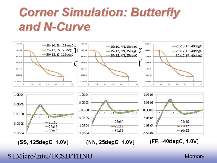
Corner Simulation: Butterfly and N-Curve • Three candidate layouts across operating corners show little difference (SS, 125 deg. C, 1. 0 V) (NN, 25 deg. C, 1. 0 V) EE 141 STMicro/Intel/UCSD/THNU (FF, -40 deg. C, 1. 0 V) 73 Memory
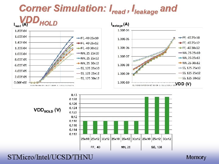
Corner Simulation: Iread , Ileakage and VDDHOLD I (A) Iread leakage VDD (V) VDDHOLD (V) EE 141 STMicro/Intel/UCSD/THNU 74 Memory
683ab4d2583d091fe16a5ba208d51f53.ppt