ce1324714af64271b324d99eb57e6591.ppt
- Количество слайдов: 10
Are classical design flows suitable below 0. 18 m? ISPD 2001 Wolfgang Roethig Senior Engineering Manager EDA R&D Group NEC Electronics Inc. WR 0999. ppt-
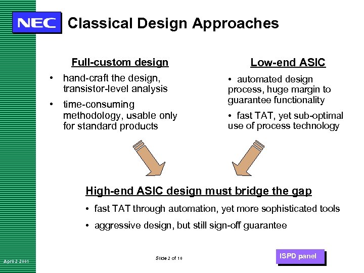
Classical Design Approaches Full-custom design • hand-craft the design, transistor-level analysis • time-consuming methodology, usable only for standard products Low-end ASIC • automated design process, huge margin to guarantee functionality • fast TAT, yet sub-optimal use of process technology High-end ASIC design must bridge the gap • fast TAT through automation, yet more sophisticated tools • aggressive design, but still sign-off guarantee April 2 2001 Slide 2 of 10 ISPD panel
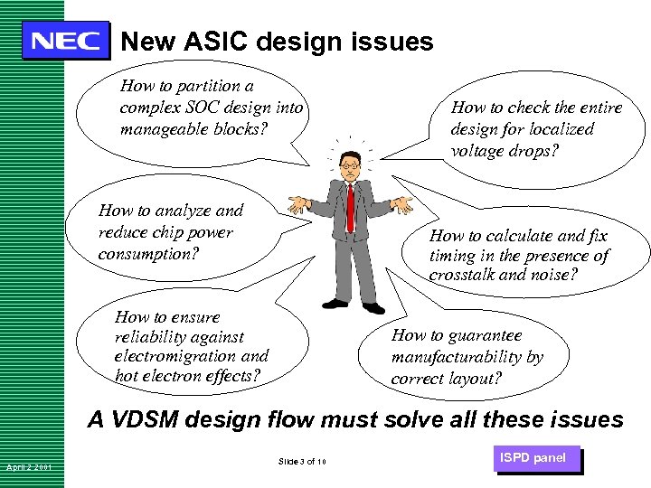
New ASIC design issues How to partition a complex SOC design into manageable blocks? How to analyze and reduce chip power consumption? How to check the entire design for localized voltage drops? How to calculate and fix timing in the presence of crosstalk and noise? How to ensure reliability against electromigration and hot electron effects? How to guarantee manufacturability by correct layout? A VDSM design flow must solve all these issues April 2 2001 Slide 3 of 10 ISPD panel
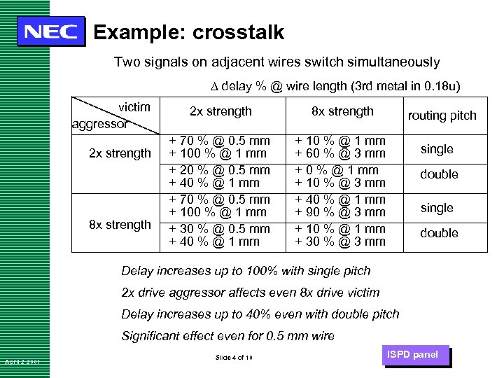
Example: crosstalk Two signals on adjacent wires switch simultaneously D delay % @ wire length (3 rd metal in 0. 18 u) victim aggressor 2 x strength 8 x strength + 70 % @ 0. 5 mm + 100 % @ 1 mm + 20 % @ 0. 5 mm + 40 % @ 1 mm + 70 % @ 0. 5 mm + 100 % @ 1 mm + 30 % @ 0. 5 mm + 40 % @ 1 mm + 10 % @ 1 mm + 60 % @ 3 mm + 0 % @ 1 mm + 10 % @ 3 mm + 40 % @ 1 mm + 90 % @ 3 mm + 10 % @ 1 mm + 30 % @ 3 mm routing pitch single double Delay increases up to 100% with single pitch 2 x drive aggressor affects even 8 x drive victim Delay increases up to 40% even with double pitch Significant effect even for 0. 5 mm wire April 2 2001 Slide 4 of 10 ISPD panel
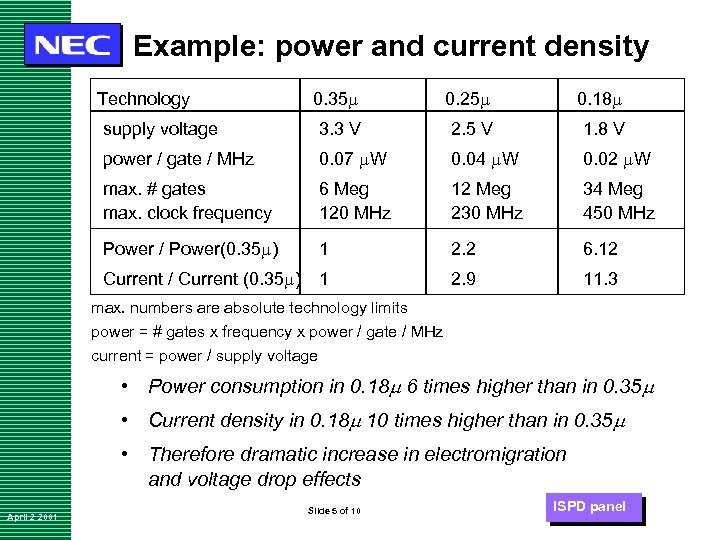
Example: power and current density 0. 35 m 0. 25 m 0. 18 m supply voltage 3. 3 V 2. 5 V 1. 8 V power / gate / MHz 0. 07 m. W 0. 04 m. W 0. 02 m. W max. # gates max. clock frequency 6 Meg 120 MHz 12 Meg 230 MHz 34 Meg 450 MHz Power / Power(0. 35 m) 1 2. 2 6. 12 Current / Current (0. 35 m) 1 2. 9 11. 3 Technology max. numbers are absolute technology limits power = # gates x frequency x power / gate / MHz current = power / supply voltage • Power consumption in 0. 18 m 6 times higher than in 0. 35 m • Current density in 0. 18 m 10 times higher than in 0. 35 m • Therefore dramatic increase in electromigration and voltage drop effects April 2 2001 Slide 5 of 10 ISPD panel
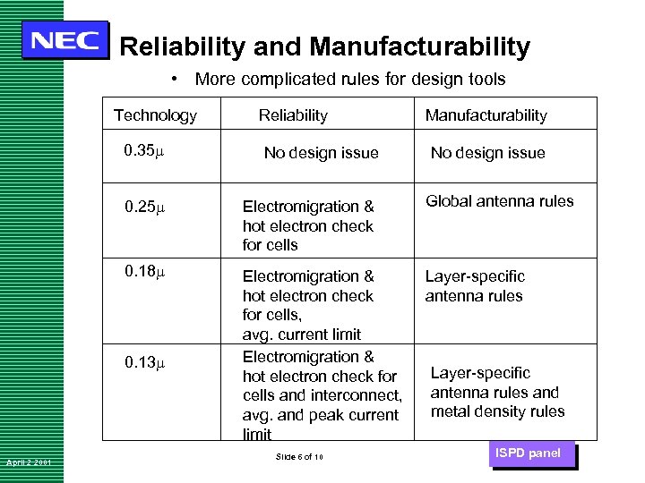
Reliability and Manufacturability • More complicated rules for design tools Technology Reliability Manufacturability 0. 35 m No design issue 0. 25 m Electromigration & hot electron check for cells Global antenna rules 0. 18 m Electromigration & hot electron check for cells, avg. current limit Electromigration & hot electron check for cells and interconnect, avg. and peak current limit Layer-specific antenna rules 0. 13 m April 2 2001 Slide 6 of 10 No design issue Layer-specific antenna rules and metal density rules ISPD panel
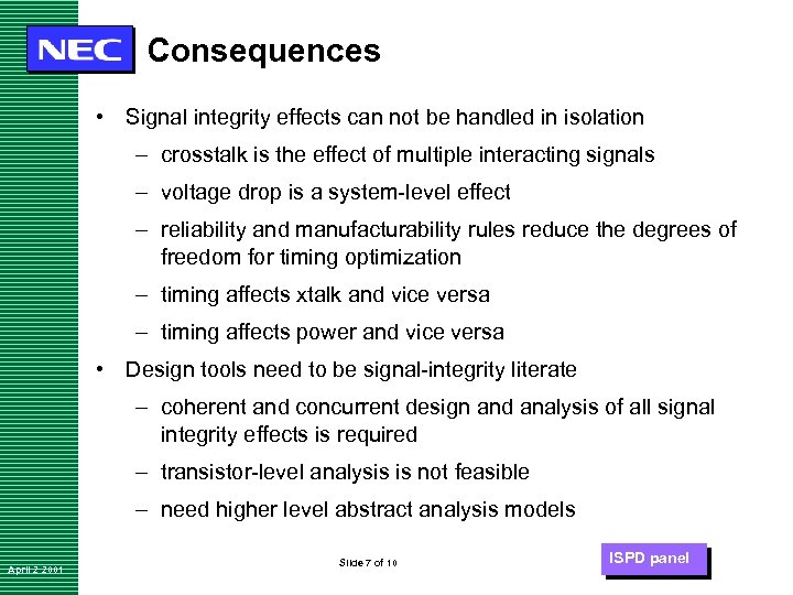
Consequences • Signal integrity effects can not be handled in isolation – crosstalk is the effect of multiple interacting signals – voltage drop is a system-level effect – reliability and manufacturability rules reduce the degrees of freedom for timing optimization – timing affects xtalk and vice versa – timing affects power and vice versa • Design tools need to be signal-integrity literate – coherent and concurrent design and analysis of all signal integrity effects is required – transistor-level analysis is not feasible – need higher level abstract analysis models April 2 2001 Slide 7 of 10 ISPD panel
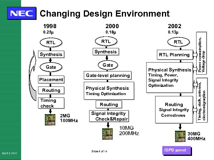
Changing Design Environment 2002 0. 25 m 0. 18 m 0. 13 m RTL Synthesis RTL Planning Gate Placement Routing Timing check Physical Synthesis Gate-level planning Physical Synthesis Timing Optimization Routing 2 MG 100 MHz Timing, Power, Signal Integrity Optimization Routing Signal Integrity Check&Repair Signal Integrity Correctness 10 MG 200 MHz April 2 2001 Slide 8 of 10 Power consumption, Voltage drop 2000 Timing, xtalk, antenna, electromigraqtion 1998 30 MG 400 MHz ISPD panel
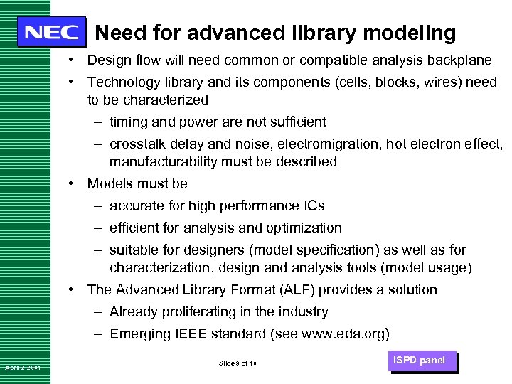
Need for advanced library modeling • Design flow will need common or compatible analysis backplane • Technology library and its components (cells, blocks, wires) need to be characterized – timing and power are not sufficient – crosstalk delay and noise, electromigration, hot electron effect, manufacturability must be described • Models must be – accurate for high performance ICs – efficient for analysis and optimization – suitable for designers (model specification) as well as for characterization, design and analysis tools (model usage) • The Advanced Library Format (ALF) provides a solution – Already proliferating in the industry – Emerging IEEE standard (see www. eda. org) April 2 2001 Slide 9 of 10 ISPD panel
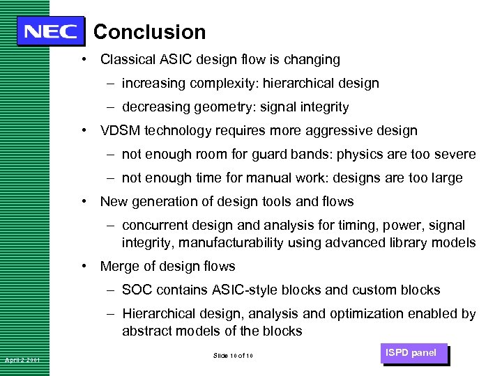
Conclusion • Classical ASIC design flow is changing – increasing complexity: hierarchical design – decreasing geometry: signal integrity • VDSM technology requires more aggressive design – not enough room for guard bands: physics are too severe – not enough time for manual work: designs are too large • New generation of design tools and flows – concurrent design and analysis for timing, power, signal integrity, manufacturability using advanced library models • Merge of design flows – SOC contains ASIC-style blocks and custom blocks – Hierarchical design, analysis and optimization enabled by abstract models of the blocks April 2 2001 Slide 10 of 10 ISPD panel
ce1324714af64271b324d99eb57e6591.ppt