Part II_Detectors_EPMA_Version 2.pptx
- Количество слайдов: 23
 Applications of X-rays to Geology Part II. X-ray registration. EDS, SEM, EPMA.
 Part II. X-ray registration. SEM, EDS, EPMA and XRF analyses. • Registrations of X-rays • Energy dispersive X-ray analysis • Scanning electron microscopy • Electron probe microanalysis • Automated mineralogy and petrography
 Registrations of X-rays Types of X-ray Detectors • Gas detectors • Scintillation counters • Solid state detectors • Charge coupled device detectors http: //imagine. gsfc. nasa. gov/docs/science/how_l 1/xray_detectors. html
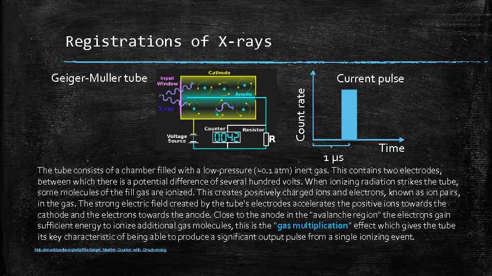 Registrations of X-rays Geiger-Muller tube Count rate Current pulse 1 µs Time The tube consists of a chamber filled with a low-pressure (~0. 1 atm) inert gas. This contains two electrodes, between which there is a potential difference of several hundred volts. When ionizing radiation strikes the tube, some molecules of the fill gas are ionized. This creates positively charged ions and electrons, known as ion pairs, in the gas. The strong electric field created by the tube's electrodes accelerates the positive ions towards the cathode and the electrons towards the anode. Close to the anode in the "avalanche region" the electrons gain sufficient energy to ionize additional gas molecules, this is the "gas multiplication" effect which gives the tube its key characteristic of being able to produce a significant output pulse from a single ionizing event. http: //en. wikipedia. org/wiki/File: Geiger_Mueller_Counter_with_Circuit-en. svg
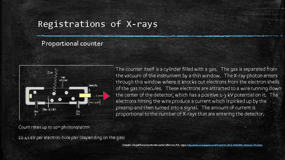 Registrations of X-rays Proportional counter The counter itself is a cylinder filled with a gas. The gas is separated from the vacuum of the instrument by a thin window. The X-ray photon enters through this window where it knocks out electrons from the electron shells of the gas molecules. These electrons are attracted to a wire running down the center of the detector, which has a positive 1 -3 k. V potential on it. The electrons hitting the wire produce a current which is picked up by the preamp and then turned into a signal. The amount of current is proportional to the number of X-rays that are entering the detector. Count rates up to 1011 photons/s/cm 3 22 -41 e. V per electron-hole pair (depending on the gas) Diagram of a gas flow proportional counter (after Lee, R. E. , 1992). http: //www. mcswiggen. com/FAQs/FAQ_EF-6_Fldr/WDS_Detector_Pict. htm
 Scintillation counters Scintillating crystals Na. J (Tl) ≈40 photons/ke. V • Na. I(Tl), Yttrium Aluminum Perovskite (YAP) or plastic which, absorb x-rays and fluoresce in the visible spectrum. • Light strikes a thin photocathode which emits electrons into the vacuum portion of a photomultiplier tube. • Photoelectrons are accelerated in steps, striking dynodes and becoming amplified. • Output voltage pulse is proportional to initial x-ray energy.
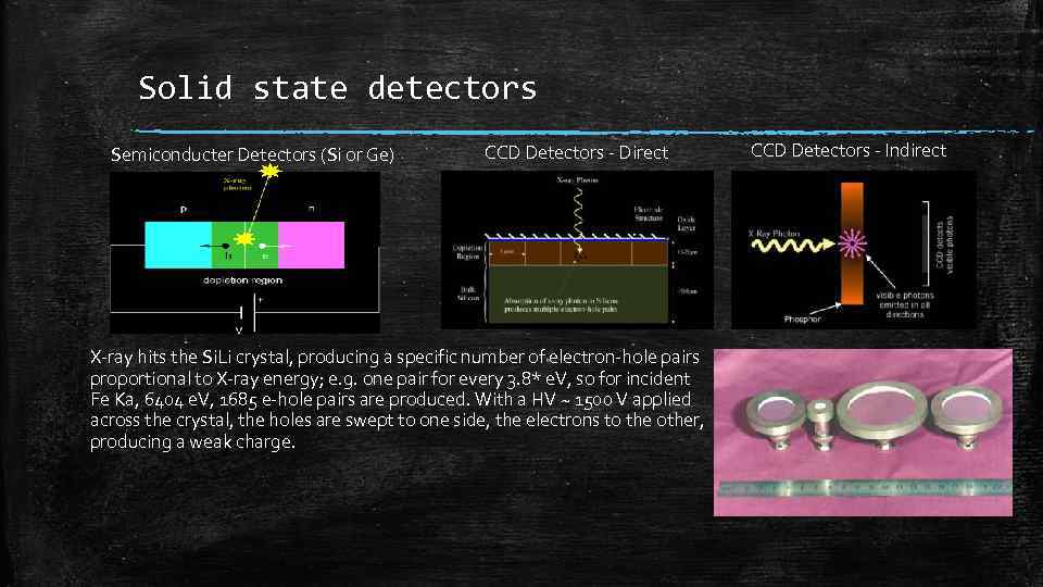 Solid state detectors Semiconducter Detectors (Si or Ge) CCD Detectors - Direct X-ray hits the Si. Li crystal, producing a specific number of electron-hole pairs proportional to X-ray energy; e. g. one pair for every 3. 8* e. V, so for incident Fe Ka, 6404 e. V, 1685 e-hole pairs are produced. With a HV ~ 1500 V applied across the crystal, the holes are swept to one side, the electrons to the other, producing a weak charge. CCD Detectors - Indirect
 CCDs for very high spatial resolution Schematic of a flat-panel detector Digital X-ray detector and two different types of scintillator. (a) Schematic illustration of an indirect conversion type X-ray image detector. (b) Sketch of the conventional scintillator. (c) Sketch of a pixel-structured scintillator. http: //www. opticsinfobase. org/oe/fulltext. cfm? uri=oe-18 -14 -14850&id=202884
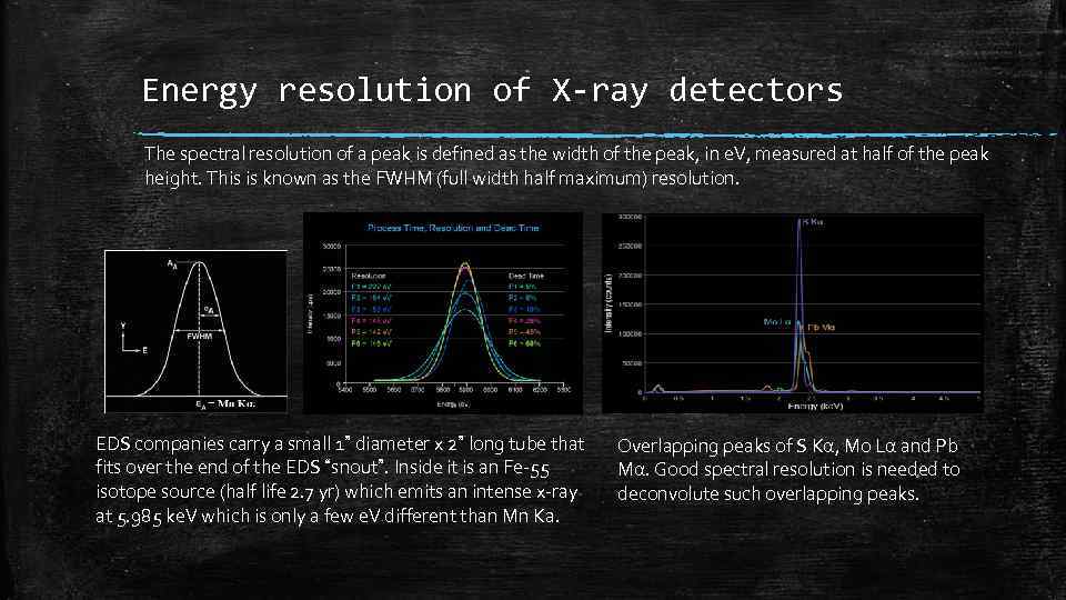 Energy resolution of X-ray detectors The spectral resolution of a peak is defined as the width of the peak, in e. V, measured at half of the peak height. This is known as the FWHM (full width half maximum) resolution. EDS companies carry a small 1” diameter x 2” long tube that fits over the end of the EDS “snout”. Inside it is an Fe-55 isotope source (half life 2. 7 yr) which emits an intense x-ray at 5. 985 ke. V which is only a few e. V different than Mn Ka. Overlapping peaks of S Kα, Mo Lα and Pb Mα. Good spectral resolution is needed to deconvolute such overlapping peaks.
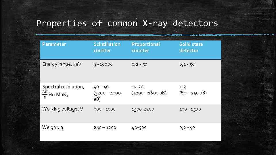 Properties of common X-ray detectors Parameter Scintillation counter Proportional counter Solid state detector Energy range, ke. V 3 - 10000 0. 2 - 50 0, 1 - 50 40 – 50 (3200 – 4000 э. В) 15 -20 (1200 – 1600 э. В) 1 -3 (80 – 240 э. В) Working voltage, V 600 - 1000 1500 -2200 100 - 1500 Weight, g 250 – 1200 40 -900 0, 2 - 50
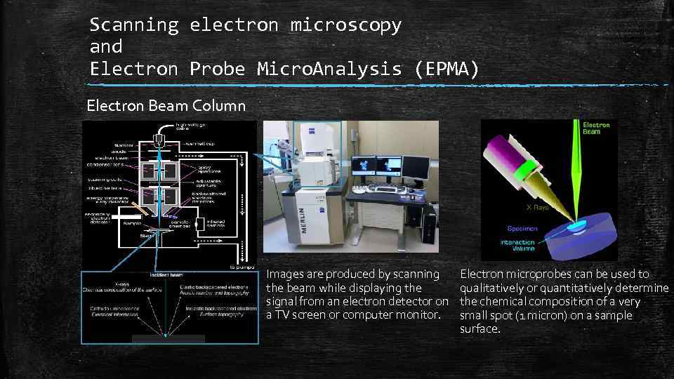 Scanning electron microscopy and Electron Probe Micro. Analysis (EPMA) Electron Beam Column Images are produced by scanning the beam while displaying the signal from an electron detector on a TV screen or computer monitor. Electron microprobes can be used to qualitatively or quantitatively determine the chemical composition of a very small spot (1 micron) on a sample surface.
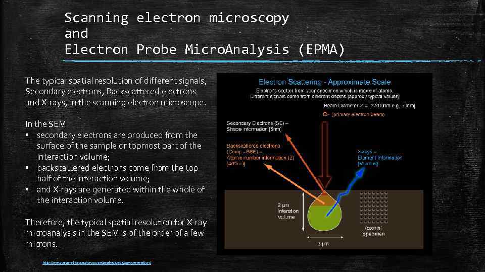 Scanning electron microscopy and Electron Probe Micro. Analysis (EPMA) The typical spatial resolution of different signals, Secondary electrons, Backscattered electrons and X-rays, in the scanning electron microscope. In the SEM • secondary electrons are produced from the surface of the sample or topmost part of the interaction volume; • backscattered electrons come from the top half of the interaction volume; • and X-rays are generated within the whole of the interaction volume. Therefore, the typical spatial resolution for X-ray microanalysis in the SEM is of the order of a few microns. http: //www. ammrf. org. au/myscope/analysis/eds/xraygeneration/
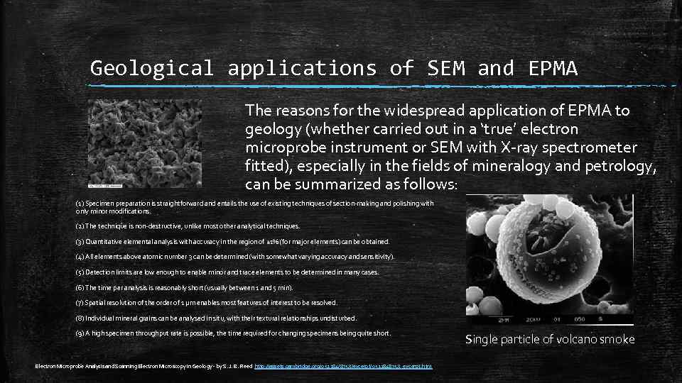 Geological applications of SEM and EPMA The reasons for the widespread application of EPMA to geology (whether carried out in a ‘true’ electron microprobe instrument or SEM with X-ray spectrometer fitted), especially in the fields of mineralogy and petrology, can be summarized as follows: (1) Specimen preparation is straightforward and entails the use of existing techniques of section-making and polishing with only minor modifications. (2) The technique is non-destructive, unlike most other analytical techniques. (3) Quantitative elemental analysis with accuracy in the region of ± 1% (for major elements) can be obtained. (4) All elements above atomic number 3 can be determined (with somewhat varying accuracy and sensitivity). (5) Detection limits are low enough to enable minor and trace elements to be determined in many cases. (6) The time per analysis is reasonably short (usually between 1 and 5 min). (7) Spatial resolution of the order of 1 μm enables most features of interest to be resolved. (8) Individual mineral grains can be analysed in situ, with their textural relationships undisturbed. (9) A high specimen throughput rate is possible, the time required for changing specimens being quite short. Electron Microprobe Analysis and Scanning Electron Microscopy in Geology - by S. J. B. Reed http: //assets. cambridge. org/052184/875 X/excerpt/052184875 X_excerpt. htm Single particle of volcano smoke
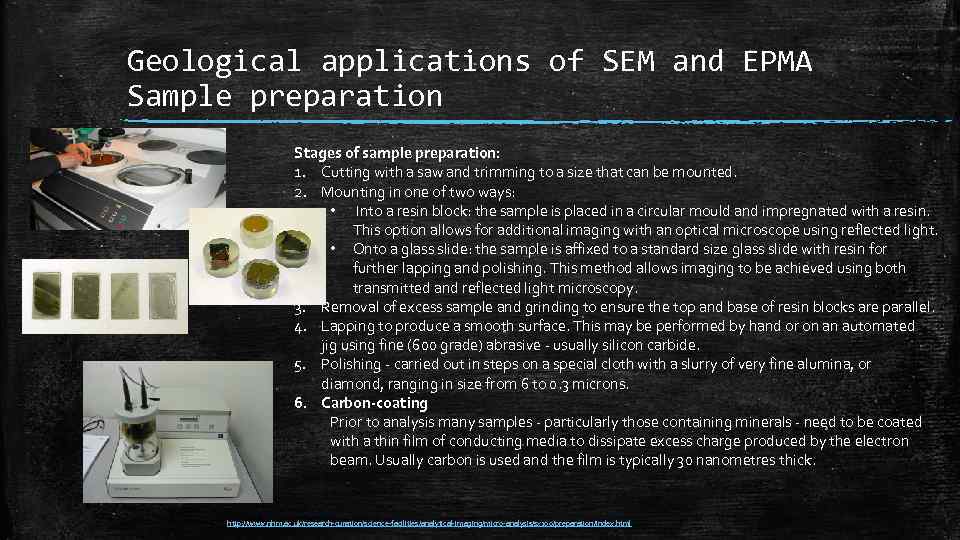 Geological applications of SEM and EPMA Sample preparation Stages of sample preparation: 1. Cutting with a saw and trimming to a size that can be mounted. 2. Mounting in one of two ways: • Into a resin block: the sample is placed in a circular mould and impregnated with a resin. This option allows for additional imaging with an optical microscope using reflected light. • Onto a glass slide: the sample is affixed to a standard size glass slide with resin for further lapping and polishing. This method allows imaging to be achieved using both transmitted and reflected light microscopy. 3. Removal of excess sample and grinding to ensure the top and base of resin blocks are parallel. 4. Lapping to produce a smooth surface. This may be performed by hand or on an automated jig using fine (600 grade) abrasive - usually silicon carbide. 5. Polishing - carried out in steps on a special cloth with a slurry of very fine alumina, or diamond, ranging in size from 6 to 0. 3 microns. 6. Carbon-coating Prior to analysis many samples - particularly those containing minerals - need to be coated with a thin film of conducting media to dissipate excess charge produced by the electron beam. Usually carbon is used and the film is typically 30 nanometres thick. http: //www. nhm. ac. uk/research-curation/science-facilities/analytical-imaging/micro-analysis/sx 100/preparation/index. html
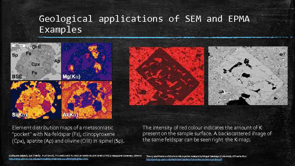 Geological applications of SEM and EPMA Examples Element distribution maps of a metasomatic "pocket" with Na-feldspar (Fs), clinopyroxene (Cpx), apatite (Ap) and olivine (Ol. II) in spinel (Sp). Guillaume Delpech, Sue O'Reilly. PLATEAUS, PLUMES AND FLUIDS IN KERGUELEN XENOLITHS // Macquarie University, GEMOC http: //www. gemoc. mq. edu. au/Annualreport/annrep 2001/Reshighlights 01. htm The intensity of red colour indicates the amount of K present on the sample surface. A backscattered image of the same feldspar can be seen right the K-map. Theory and Practice of Electron Microprobe Analysis by Miguel Santiago // University of Puerto Rico http: //geology. uprm. edu/facilities/Class%20 Forms/electronmicroprobe. pdf
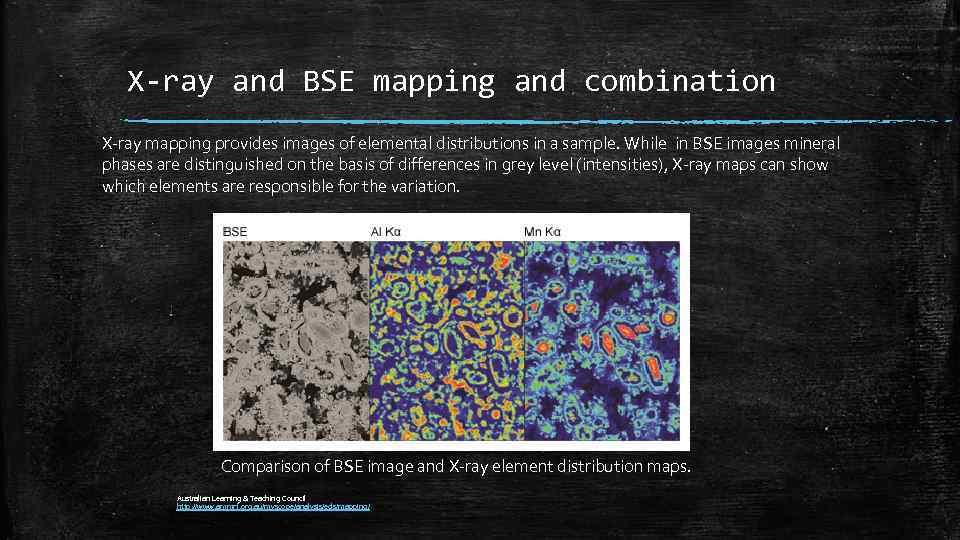 X-ray and BSE mapping and combination X-ray mapping provides images of elemental distributions in a sample. While in BSE images mineral phases are distinguished on the basis of differences in grey level (intensities), X-ray maps can show which elements are responsible for the variation. Comparison of BSE image and X-ray element distribution maps. Australian Learning & Teaching Council http: //www. ammrf. org. au/myscope/analysis/eds/mapping/
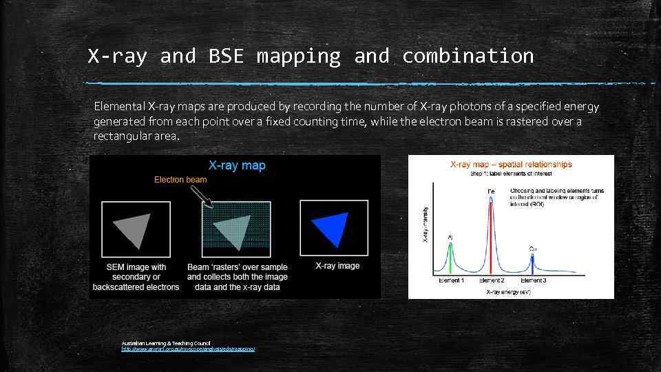 X-ray and BSE mapping and combination Elemental X-ray maps are produced by recording the number of X-ray photons of a specified energy generated from each point over a fixed counting time, while the electron beam is rastered over a rectangular area. Australian Learning & Teaching Council http: //www. ammrf. org. au/myscope/analysis/eds/mapping/
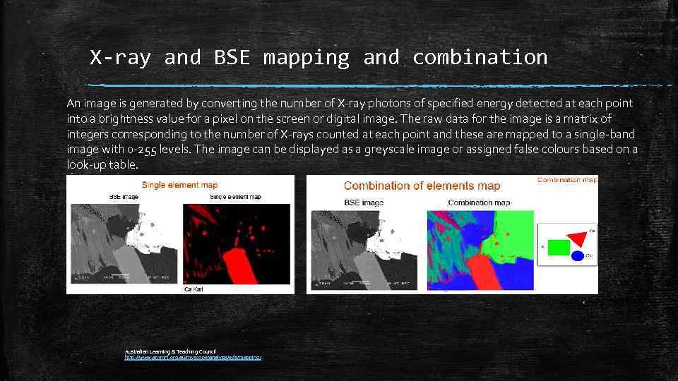 X-ray and BSE mapping and combination An image is generated by converting the number of X-ray photons of specified energy detected at each point into a brightness value for a pixel on the screen or digital image. The raw data for the image is a matrix of integers corresponding to the number of X-rays counted at each point and these are mapped to a single-band image with 0 -255 levels. The image can be displayed as a greyscale image or assigned false colours based on a look-up table. Australian Learning & Teaching Council http: //www. ammrf. org. au/myscope/analysis/eds/mapping/
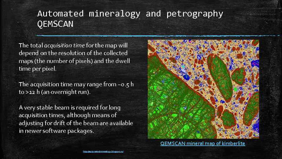 Automated mineralogy and petrography QEMSCAN The total acquisition time for the map will depend on the resolution of the collected maps (the number of pixels) and the dwell time per pixel. The acquisition time may range from ~0. 5 h to >12 h (an overnight run). A very stable beam is required for long acquisition times, although means of adjusting for drift of the beam are available in newer software packages. QEMSCAN mineral map of kimberlite http: //automatedmineralogy. blogspot. ru/
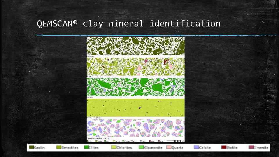 QEMSCAN® clay mineral identification http: //automatedmineralogy. blogspot. ru/
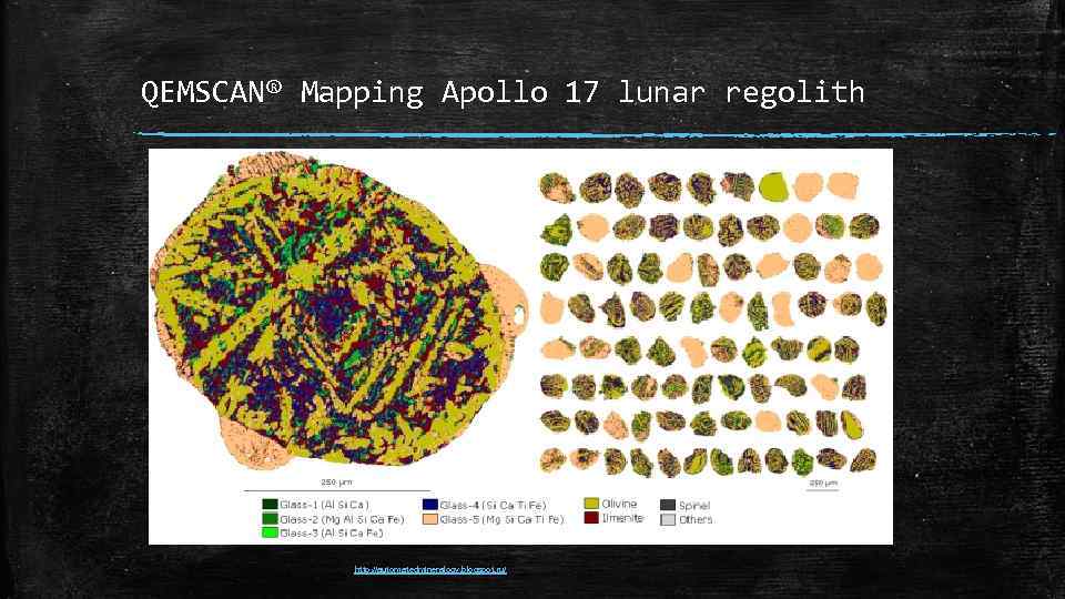 QEMSCAN® Mapping Apollo 17 lunar regolith http: //automatedmineralogy. blogspot. ru/
 Reference Books
 Summary • Some common principles used to detect X-rays include the ionization of gas, the conversion to visible light in a scintillator and the production of electron-hole pairs in a semiconductor detector. • A wide variety of x-ray detectors is available, some counting single photons, some providing only measurements of count rate or total flux, others measuring the energy, position, and/or incidence time of each x-ray. • Solid state detectors with high energy resolution allow to perform elemental analysis of geological samples • SEM uses a focused beam of electrons to image the sample, its spatial resolution in the SE images is less than 1 µm. • Sample preparation for SEM usually includes sample polishing and sputter coating with metals or carbon. Suitable samples include most solids which are stable under vacuum. • Secondary electrons, Backscattered electrons and X-rays signals in SEM have different spatial resolution. • Mineral phases are distinguished largely by their grey levels (intensities) in the BSE image


