6f049b3b486e43106baa76c98d170cf7.ppt
- Количество слайдов: 21
 Announcements • Assignment 8 posted – Due Friday Dec 2 nd. A bit longer than others. • Project progress? • Dates – Thursday 12/1 review lecture – Tuesday 12/6 project demonstrations in the lab (no presentations) – Sunday 12/11 project reports due to me by email – Tuesday 12/13 final exam, 1 pm-3 pm here.
 Last Topic! • Analog / Digital Conversion
 Introduction • Most signals are naturally analog (e. g. a voltage) • Digital techniques are often more useful: data storage, processing, computing, error free signal transmission etc. • We need ways to convert analog signals to digital • Want A/D converters to be fast, accurate and cheap • There are various methods of analog to digital conversion • Digital to analog conversion is also important: e. g. CRT video monitors convert computer generated digital information into analog signals used to guide an electron beam. MP 3 players convert music stored digitally into analog signals to drive an amplifier and speaker. • Digital to analog conversion is an integral part of some types of analog to digital converters
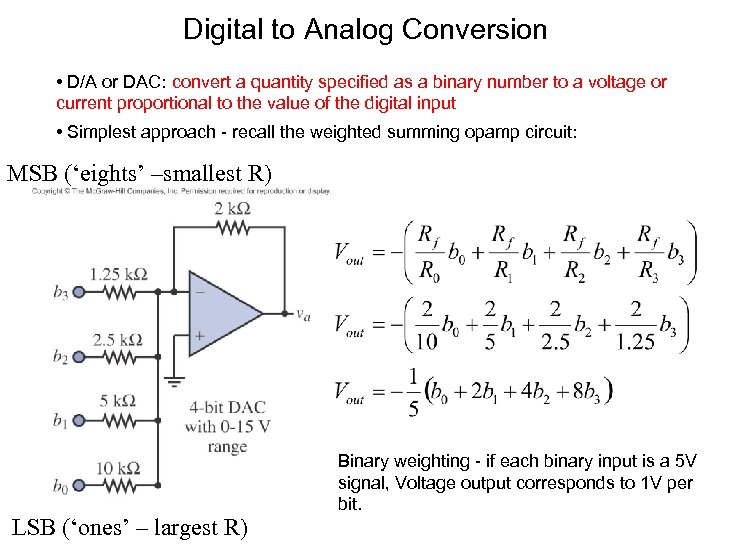 Digital to Analog Conversion • D/A or DAC: convert a quantity specified as a binary number to a voltage or current proportional to the value of the digital input • Simplest approach - recall the weighted summing opamp circuit: MSB (‘eights’ –smallest R) LSB (‘ones’ – largest R) Binary weighting - if each binary input is a 5 V signal, Voltage output corresponds to 1 V per bit.
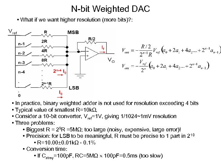 N-bit Weighted DAC • What if we want higher resolution (more bits)? : • In practice, binary weighted adder is not used for resolution exceeding 4 bits • Typical value of smallest R=10 kΩ, • Consider a 10 -bit converter, Vref=1 V, giving 1/1024~1 m. V resolution • Three problems: • Biggest R = 29 R =5 MΩ; too large (noisy, expensive, large error)! • Precision: for LSB to be meaningful, R must be precise to 1 part in 210 • R=10. 00± 0. 01 kΩ - 0. 1% • Conversion time: • If Cstray=100 p. F, RC=5 MΩ 100 p. F=0. 5 ms (too slow)
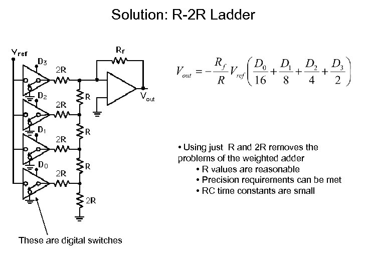 Solution: R-2 R Ladder Vout • Using just R and 2 R removes the problems of the weighted adder • R values are reasonable • Precision requirements can be met • RC time constants are small These are digital switches
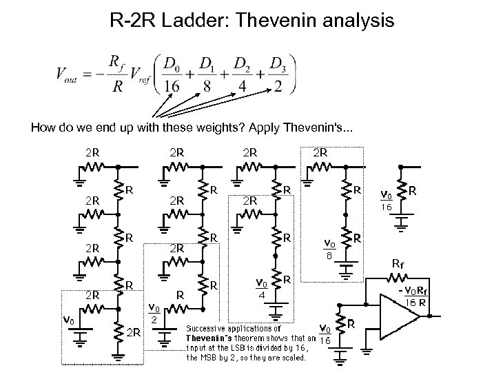 R-2 R Ladder: Thevenin analysis How do we end up with these weights? Apply Thevenin's. . .
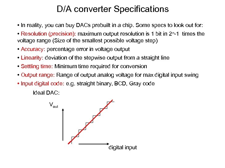 D/A converter Specifications • In reality, you can buy DACs prebuilt in a chip. Some specs to look out for: • Resolution (precision): maximum output resolution is 1 bit in 2 n-1 times the voltage range (Size of the smallest possible voltage step) • Accuracy: percentage error in voltage output • Linearity: deviation of the stepwise output from a straight line • Settling time: Minimum time required for conversion • Output range: Range of output analog voltage for max digital input swing • Input digital code: e. g. straight binary, BCD, Gray code Ideal DAC: Vout digital input
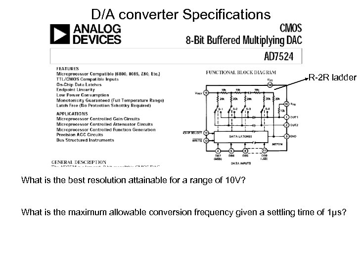 D/A converter Specifications R-2 R ladder What is the best resolution attainable for a range of 10 V? What is the maximum allowable conversion frequency given a settling time of 1μs?
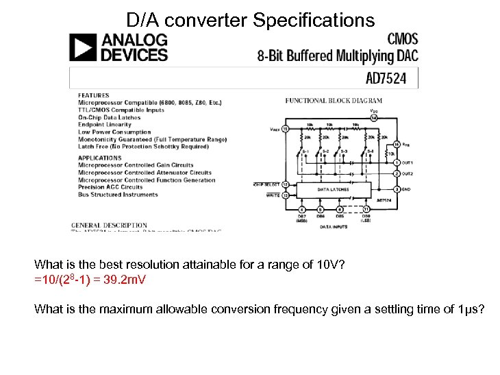 D/A converter Specifications What is the best resolution attainable for a range of 10 V? =10/(28 -1) = 39. 2 m. V What is the maximum allowable conversion frequency given a settling time of 1μs?
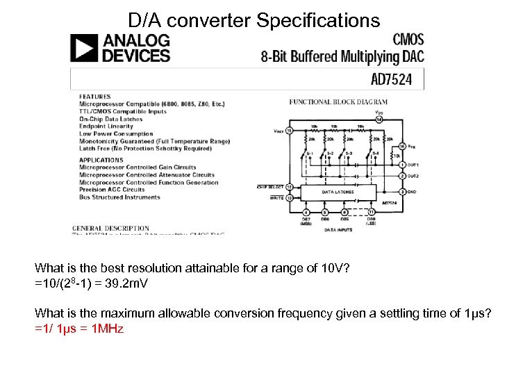 D/A converter Specifications What is the best resolution attainable for a range of 10 V? =10/(28 -1) = 39. 2 m. V What is the maximum allowable conversion frequency given a settling time of 1μs? =1/ 1μs = 1 MHz
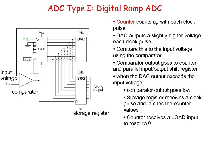 ADC Type I: Digital Ramp ADC input voltage comparator • Counter counts up with each clock pulse • DAC outputs a slightly higher voltage each clock pulse • Compare this to the input voltage using the comparator • Comparator output goes to counter and parallel input/output shift register • when the DAC output exceeds the input voltage • comparator output goes low • Storage register receives a clock pulse and latches the counter values storage register • Counter receives a LOAD input to reset to 0
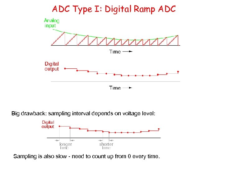 ADC Type I: Digital Ramp ADC Big drawback: sampling interval depends on voltage level: Sampling is also slow - need to count up from 0 every time.
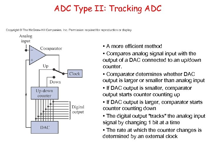 ADC Type II: Tracking ADC • A more efficient method • Compares analog signal input with the output of a DAC connected to an up/down counter. • Comparator determines whether DAC output is larger or smaller than analog input • If DAC output is smaller, comparator output starts counter counting up • If DAC output is larger, comparator starts counter counting down • The digital output "tracks" the analog input signal by changing 1 bit at a time • The rate at which the counter changes is determined by an external clock
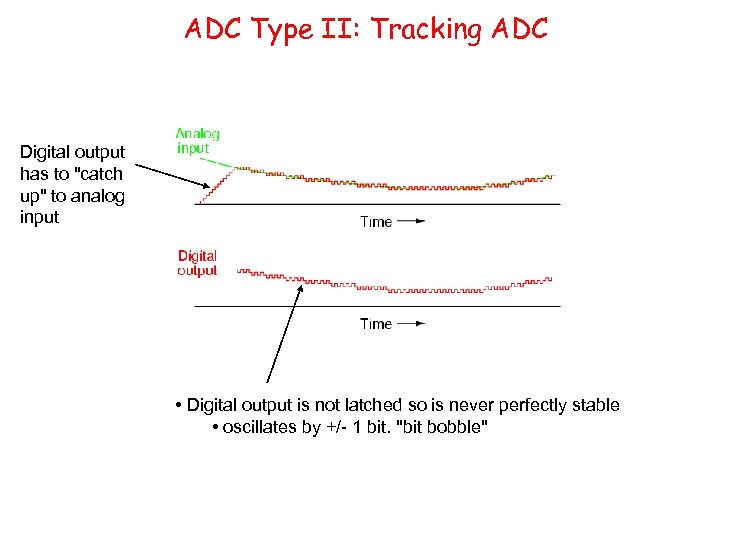 ADC Type II: Tracking ADC Digital output has to "catch up" to analog input • Digital output is not latched so is never perfectly stable • oscillates by +/- 1 bit. "bit bobble"
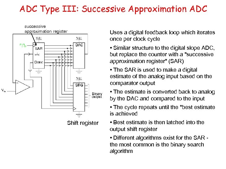 ADC Type III: Successive Approximation ADC successive approximation register Uses a digital feedback loop which iterates once per clock cycle • Similar structure to the digital slope ADC, but replace the counter with a "successive approximation register" (SAR) • The SAR is used to make a digital estimate of the analog input based on the comparator output • The estimate is converted back to analog by the DAC and compared to the input • The cycle repeats until the "best estimate is achieved Shift register • Best estimate is then latched into the output shift register • Different algorithms exist for the SAR the most common is the binary search algorithm
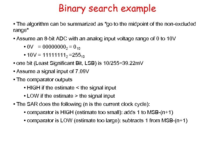 Binary search example • The algorithm can be summarized as "go to the midpoint of the non-excluded range" • Assume an 8 -bit ADC with an analog input voltage range of 0 to 10 V • 0 V = 00002 = 010 • 10 V = 11112 =25510 • one bit (Least Significant Bit, LSB) is 10/255=39. 22 m. V • Assume a signal input of 7. 09 V • The comparator outputs • HIGH if the estimate < the signal input • LOW if the estimate > the signal input • The SAR does the following (n is the current clock cycle): • comparator is HIGH (estimate too small): adds 1 to MSB-(n+1) • comparator is LOW (estimate too large): subtracts 1 from MSB-(n+1)
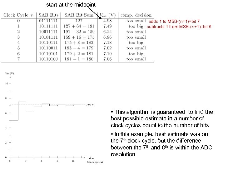 start at the midpoint adds 1 to MSB-(n+1)=bit 7 subtracts 1 from MSB-(n+1)=bit 6 • This algorithm is guaranteed to find the best possible estimate in a number of clock cycles equal to the number of bits • In this example, best estimate was on the 7 th clock cycle, but the difference between the 7 th and 8 th is within the ADC resolution
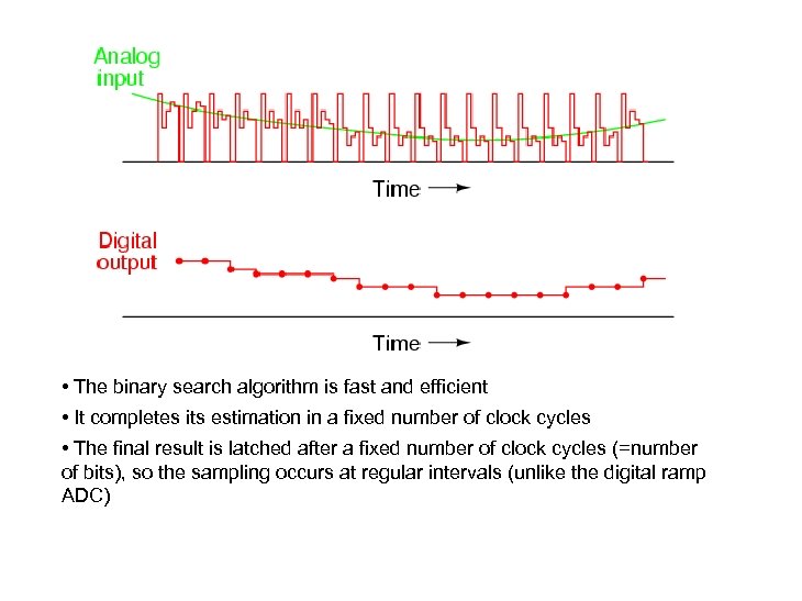 • The binary search algorithm is fast and efficient • It completes its estimation in a fixed number of clock cycles • The final result is latched after a fixed number of clock cycles (=number of bits), so the sampling occurs at regular intervals (unlike the digital ramp ADC)
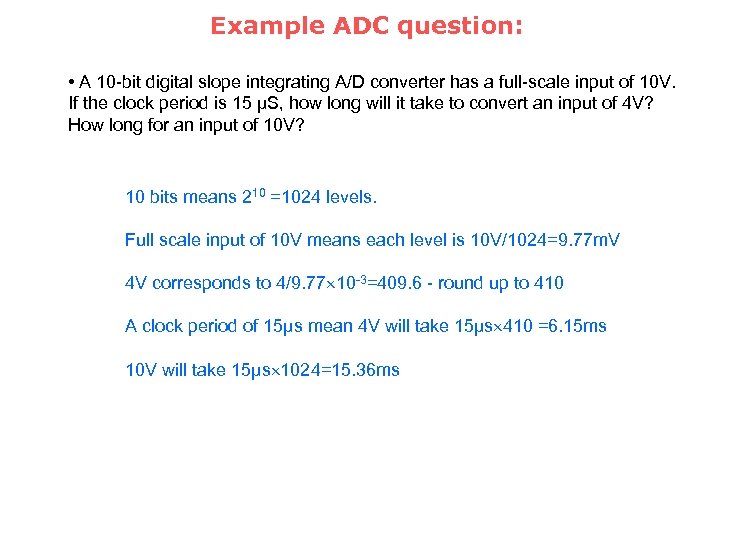 Example ADC question: • A 10 -bit digital slope integrating A/D converter has a full-scale input of 10 V. If the clock period is 15 μS, how long will it take to convert an input of 4 V? How long for an input of 10 V? 10 bits means 210 =1024 levels. Full scale input of 10 V means each level is 10 V/1024=9. 77 m. V 4 V corresponds to 4/9. 77 10 -3=409. 6 - round up to 410 A clock period of 15μs mean 4 V will take 15μs 410 =6. 15 ms 10 V will take 15μs 1024=15. 36 ms
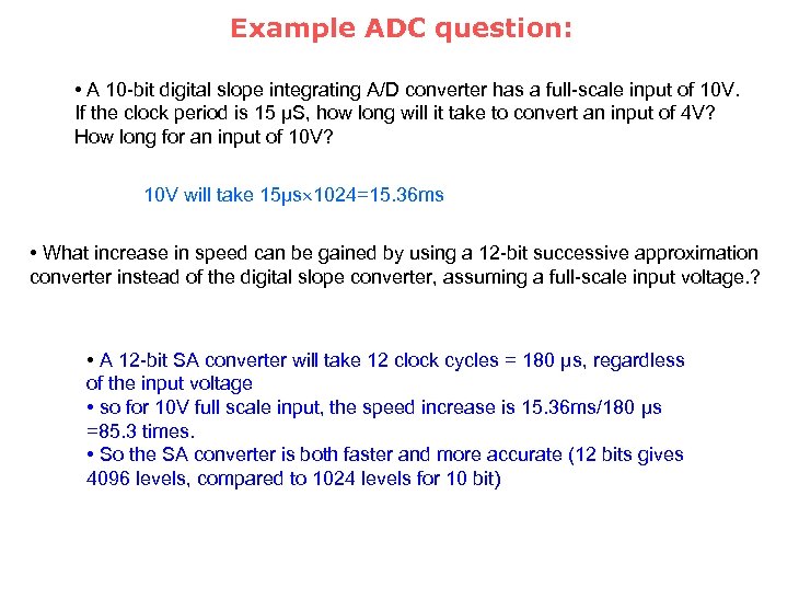 Example ADC question: • A 10 -bit digital slope integrating A/D converter has a full-scale input of 10 V. If the clock period is 15 μS, how long will it take to convert an input of 4 V? How long for an input of 10 V? 10 V will take 15μs 1024=15. 36 ms • What increase in speed can be gained by using a 12 -bit successive approximation converter instead of the digital slope converter, assuming a full-scale input voltage. ? • A 12 -bit SA converter will take 12 clock cycles = 180 μs, regardless of the input voltage • so for 10 V full scale input, the speed increase is 15. 36 ms/180 μs =85. 3 times. • So the SA converter is both faster and more accurate (12 bits gives 4096 levels, compared to 1024 levels for 10 bit)


