

ed6bd632cb7936e1efa2f3b78ec4fac1.ppt
- Количество слайдов: 41
 Analysis versus design • Analysis: – Given a system, find its properties. – The solution is unique. • Design: » Given a set of properties, come up with a system possessing them. » The solution is rarely unique.
 The IC Design Process, Allen’s view
 Texas Instruments, or Vaibhav Kumar’s view PG: pattern generation, also called tapeout, to generate GDS RTM: release to manufacturing NPD: new product development (delivery)
 Texas Instruments, or Vaibhav Kumar’s view
 Product definition & specification • Based on market study – Future market opportunities – Gaps/niches in existing products – Cost effective replacements • Customer needs to specifications – Application environment – Interfaces with other components – I/O requirements – Accuracy/linearity requirements –…
 Electrical Design • the process from the specifications to a circuit solution • Requires active and passive device electrical models for – Creating the design – Verifying the design – Determining the robustness of the design
 Physical Design • From electrical design to a layout pattern
 Test Design • To verify that fabricated circuit meets specifications • To characterize additional “behavior” • To trouble-shoot design • To fine tune certain parameters • To trim certain parameters • Top designers are top test engineers
 Skill-set for Analog IC design • • • Good physics background Decent math skills Skilled in measurements Good understanding of principles, concepts, and assumptions Skilled in simulation Grasp of technology and modeling Intuition for reasonable simplifications Audacity to try new things, but guided by theory and physics Not afraid of failure, but methodical learning from failures/mistakes Wide range of knowledge
 Technology scaling • The good: – – Smaller geometries Smaller parasitics Higher transconductance Higher bandwidths • The bad: – – Reduced voltages Smaller channel resistances (lower gain) More nonlinearity Deviation from square-law behavior • The challenging: – – Increased substrate noise in mixed signal applications Threshold voltages are not scaling with power supply Reduced dynamic range Poor matching at minimum channel length
 HW • Go to the MOSIS webpage • Find and download the NDA for IBM 0. 13 • Sign it, either give to TA in person, or scan and email to TA
 Signal naming conventions
 Schematic Symbols
 Circuit analysis skills • Please review materials in appendix A • Make sure you are fluent at – Nodal analysis, KCL – Mesh analysis (dual to nodal), KVL – Cascade stages – Small signal analysis, including linearization – Equivalent circuits – Miller simplification
 Cascade V 1 = Vout/vin =
 Nodal analysis KCL at node A: KCL at node B: Solve for Vout/Iin =
 Small signal analysis The amplifier may be nonlinear, but near an operating point, it has a small signal model of: vo = Av * vin. By definition, SSA is always linear.
 Making Equivalent substitutions Simplified Cascade
 Miller simplification If v 2 = K*v 1 i 1 = (v 1 -Kv 1)/Z =(1 -K)v 1/Z i 2 = (v 2 -v 1/K)/Z =(K-1)/K v 2/Z
 HW • Read through Appendix A. • Browse through problems 1. 1 -4 to 1. 1 -12 • If you are excellent, write a statement to indicate so. • If you are rusty on these, briefly do all of these problems and check your answers against book answers.
 BASIC FABRTICATION PROCESSES – Oxide growth – Thermal diffusion – Ion implantation – Deposition – Etching – Shallow trench isolation – Epitaxy • Photolithography
on") Oxidation • The process of growing a layer of silicon dioxide (Si. O 2)on the surface of a silicon wafer. • Uses: ü Provide isolation between two layers ü Protect underlying material from contamination ü Very thin oxides (100 to 1000 Å) are grown using dry-oxidation techniques. ü Thicker oxides (>1000 Å) are grown using wet oxidation techniques.
Oxidation • The process of growing a layer of silicon dioxide (Si. O 2)on the surface of a silicon wafer. • Uses: ü Provide isolation between two layers ü Protect underlying material from contamination ü Very thin oxides (100 to 1000 Å) are grown using dry-oxidation techniques. ü Thicker oxides (>1000 Å) are grown using wet oxidation techniques.
") (Thickness of Si. O 2 grossly exaggerated. )
(Thickness of Si. O 2 grossly exaggerated. )
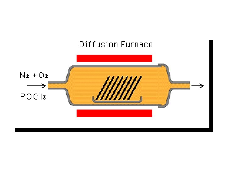
 Diffusion Movement of impurity atoms at the surface of the silicon into the bulk of the silicon - From higher concentration to lower concentration. - Done at high temperatures: 800 to 1400 °C.
 Infinite-source diffusion
 Finite-source diffusion
 Ion Implantation The process by which impurity ions are accelerated to a high velocity and physically lodged into the target.
 • Require annealing to repair damage • Can implant through surface layers • Can achieve unique doping profile
 • Low-pressure chemical-vapor deposition • Plasma-assisted chemical-vapor deposition •") Deposition • Chemical-vapor deposition (CVD) • Low-pressure chemical-vapor deposition • Plasma-assisted chemical-vapor deposition • Sputter deposition • Materials deposited – Silicon nitride (Si 3 N 4) – Silicon dioxide (Si. O 2) – Aluminum – Polysilicon
Deposition • Chemical-vapor deposition (CVD) • Low-pressure chemical-vapor deposition • Plasma-assisted chemical-vapor deposition • Sputter deposition • Materials deposited – Silicon nitride (Si 3 N 4) – Silicon dioxide (Si. O 2) – Aluminum – Polysilicon
 Etching • To selectively remove a layer of material • But may remove portions or all of – The desired material – The underlying layer – The masking layer • Two basic types of etches: – Wet etch, uses chemicals – Dry etch, uses chemically active ionized gasses.
 Wet Etching
 • Selectivity: • Anisotropy: a and b due to finite S c is due to non-unity A
 Epitaxy • Epitaxial growth consists of the formation of a layer of single-crystal silicon on the surface of the silicon material so that the crystal structure of the silicon is continuous across the interfaces. – It is done externally to the material as opposed to diffusion which is internal – The epitaxial layer (epi) can be doped differently, even opposite to the material on which it is grown – It is accomplished at high temperatures using a chemical reaction at the surface – The epi layer can be any thickness, typically 1 -20 microns
 Photolithography • Components – Photoresist material – Photomask – Material to be patterned (e. g. , Si. O 2) • Positive photoresist– Areas exposed to UV light are soluble in the developer • Negative photoresist– Areas not exposed to UV light are soluble in the developer
 Steps: 1. Apply photoresist 2. Soft bake 3. Expose the photoresist to UV light through photomask 4. Develop (remove unwanted photoresist) 5. Hard bake 6. Etch the exposed layer 7. Remove photoresist
 Expose: The process of exposing selective areas to light through a photo-mask is called printing. Types of printing include: • Contact printing • Proximity printing • Projection printing
 After Developing
 After Etching
 After Removing Photoresist
 HW For each of the following process steps, name 2 or 3 ways in which non -idealities can happen, briefly comment on how the non-ideality affect circuit parameters. – – – Oxide growth Ion implantation Deposition Etching Photolithography