9834d3c8f8e8d2ff90534baae044df2d.ppt
- Количество слайдов: 36
An Impulse-Response Based Methodology for Modeling Complex Interconnect Networks Zeynep Dilli, Neil Goldsman, Akın Aktürk Dept. of Electrical and Computer Eng. University of Maryland, College Park
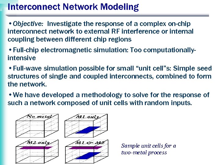
Interconnect Network Modeling • Objective: Investigate the response of a complex on-chip interconnect network to external RF interference or internal coupling between different chip regions • Full-chip electromagnetic simulation: Too computationallyintensive • Full-wave simulation possible for small “unit cell”s: Simple seed structures of single and coupled interconnects, combined to form the network. • We have developed a methodology to solve for the response of such a network composed of unit cells with random inputs. Sample unit cells for a two-metal process
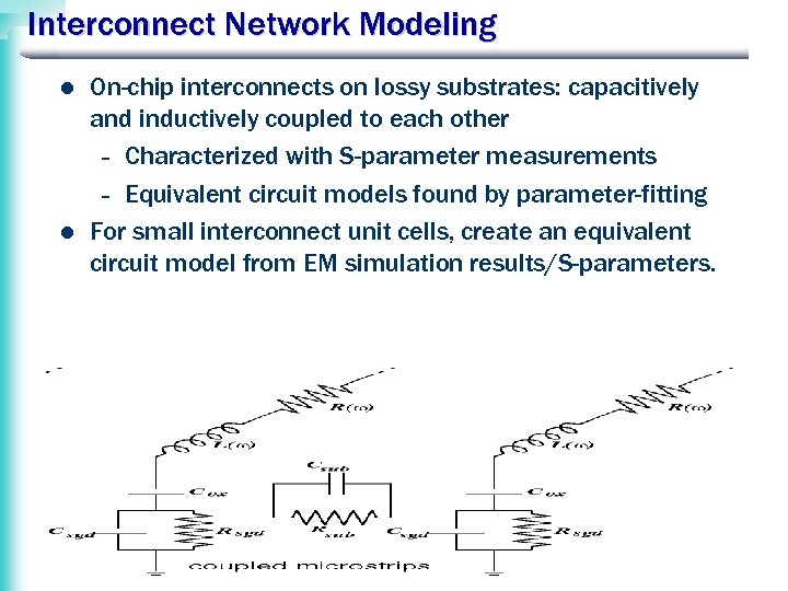
Interconnect Network Modeling l l On-chip interconnects on lossy substrates: capacitively and inductively coupled to each other – Characterized with S-parameter measurements – Equivalent circuit models found by parameter-fitting For small interconnect unit cells, create an equivalent circuit model from EM simulation results/S-parameters.
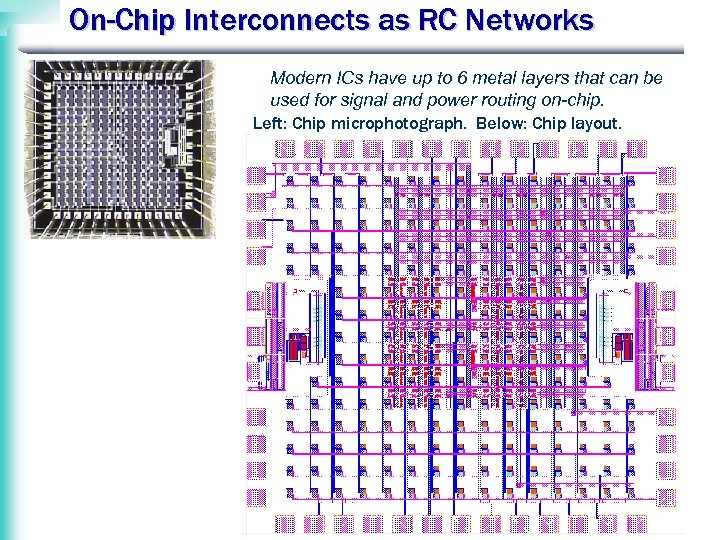
On-Chip Interconnects as RC Networks Modern ICs have up to 6 metal layers that can be used for signal and power routing on-chip. Left: Chip microphotograph. Below: Chip layout.
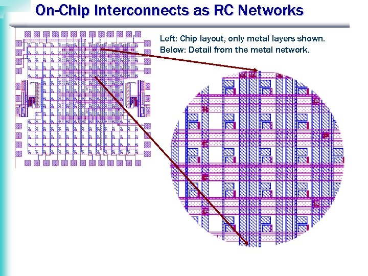
On-Chip Interconnects as RC Networks Left: Chip layout, only metal layers shown. Below: Detail from the metal network.
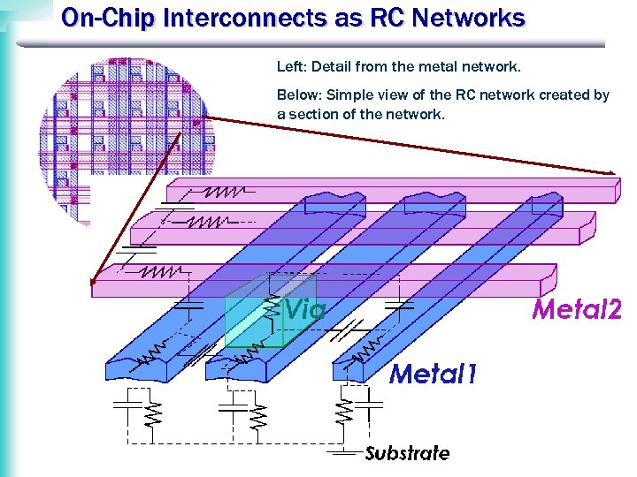
On-Chip Interconnects as RC Networks Left: Detail from the metal network. Below: Simple view of the RC network created by a section of the network.
Interconnect Network Modeling l The interconnect network is a linear time invariant system: It is straightforward to calculate the output to any input distribution in space and time from the impulse responses.
![Response to a General Input from Impulse Responses f[x, t] Define the unit impulse Response to a General Input from Impulse Responses f[x, t] Define the unit impulse](https://present5.com/presentation/9834d3c8f8e8d2ff90534baae044df2d/image-8.jpg)
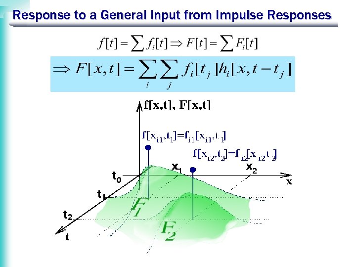
Response to a General Input from Impulse Responses f[x, t] Define the unit impulse at point xi: [xxi]= 1, x=xi 0, else We calculate the system’s impulse response: hi[x, t] [xxi] [t] Let an input f[x, t] be applied to the system. This input can be written as the superposition of time-varying input components fi[t]=f[xi, t] applied to each point xi: We can write these input components fi[t] as Writing fi[t] as the sum of a series of time-impulses marching in time:
![Response to a General Input from Impulse Responses f[x, t] Let Fi[x, t] be Response to a General Input from Impulse Responses f[x, t] Let Fi[x, t] be](https://present5.com/presentation/9834d3c8f8e8d2ff90534baae044df2d/image-9.jpg)
Response to a General Input from Impulse Responses f[x, t] Let Fi[x, t] be the system’s response to this input applied to xi: fi [t] Fi[x, t] For a time-invariant system we can use the impulse response to find Fi[x, t] : Then, since
Response to a General Input from Impulse Responses
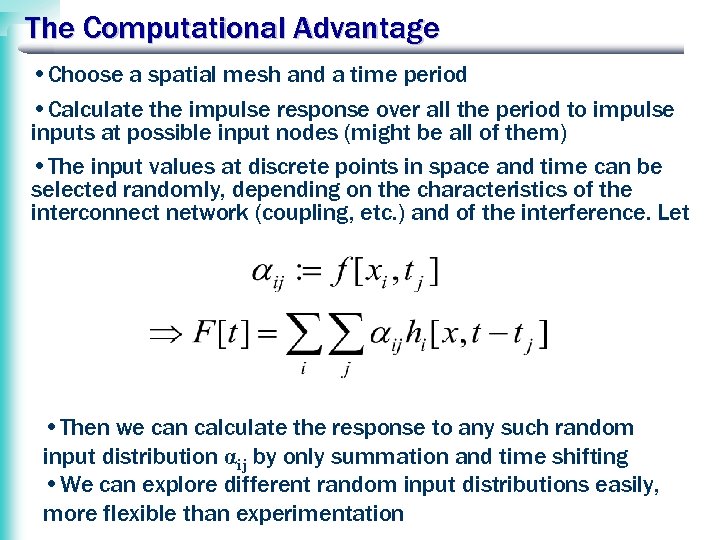
The Computational Advantage • Choose a spatial mesh and a time period • Calculate the impulse response over all the period to impulse inputs at possible input nodes (might be all of them) • The input values at discrete points in space and time can be selected randomly, depending on the characteristics of the interconnect network (coupling, etc. ) and of the interference. Let • Then we can calculate the response to any such random input distribution αij by only summation and time shifting • We can explore different random input distributions easily, more flexible than experimentation
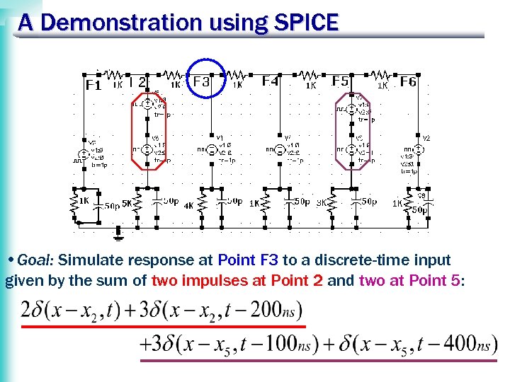
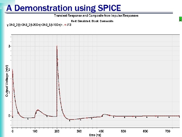
A Demonstration using SPICE • Goal: Simulate response at Point F 3 to a discrete-time input given by the sum of two impulses at Point 2 and two at Point 5:
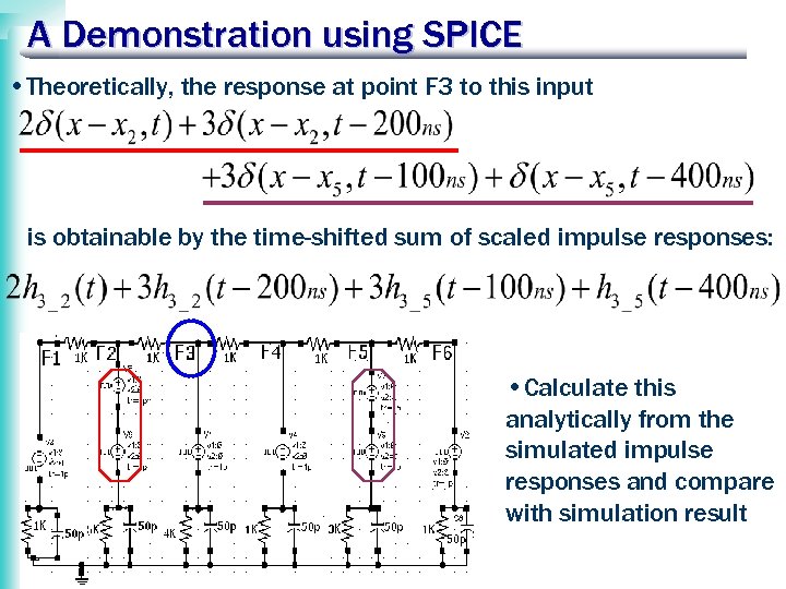
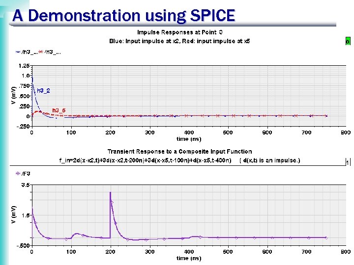
A Demonstration using SPICE • Theoretically, the response at point F 3 to this input is obtainable by the time-shifted sum of scaled impulse responses: • Calculate this analytically from the simulated impulse responses and compare with simulation result
A Demonstration using SPICE
A Demonstration using SPICE
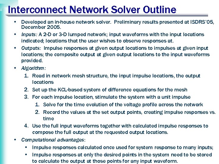
Interconnect Network Solver Outline • Developed an in-house network solver. Preliminary results presented at ISDRS’ 05, December 2005. • Inputs: A 2 -D or 3 -D lumped network; input waveforms with the input locations indicated; locations that the user wishes to observe responses at. • Outputs: Impulse responses at given output locations to impulses at given input locations; the composite output at given output locations to the input waveforms provided. • Algorithm: 1. Read in network mesh structure, the input impulse locations, the output locations 2. Set up the KCL-based system of difference equations for the mesh 3. For each impulse location, stimulate the system with a unit impulse 1. Solve for the time evolution of the voltage profile across the network 2. Record the values at the set output points, creating impulse responses vs. time 4. Use the full input waveforms together with calculated impulse responses to compose the full output at the requested output locations. • Computational advantages: • Impulse responses calculated once used for system response to many inputs; • Impulse responses at only the desired points in the system need to be stored to calculate the output at those points for any input waveform.
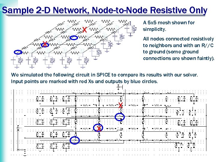
Sample 2 -D Network, Node-to-Node Resistive Only A 5 x 5 mesh shown for simplicity. All nodes connected resistively to neighbors and with an R//C to ground (some ground connections are shown faintly). We simulated the following circuit in SPICE to compare its results with our solver. Input points are marked with red Xs and outputs by blue circles.
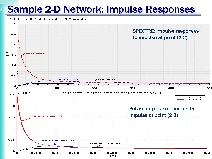
Sample 2 -D Network: Impulse Responses SPECTRE: impulse responses to impulse at point (2, 2) Solver: impulse responses to impulse at point (2, 2)
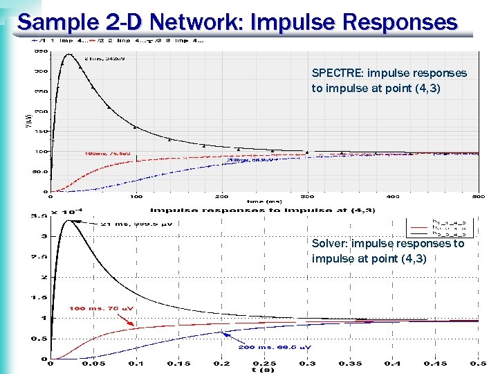
Sample 2 -D Network: Impulse Responses SPECTRE: impulse responses to impulse at point (4, 3) Solver: impulse responses to impulse at point (4, 3)
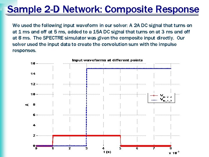
Sample 2 -D Network: Composite Response We used the following input waveform in our solver: A 2 A DC signal that turns on at 1 ms and off at 5 ms, added to a 15 A DC signal that turns on at 3 ms and off at 8 ms. The SPECTRE simulator was given the composite input directly. Our solver used the input data to create the convolution sum with the impulse responses.
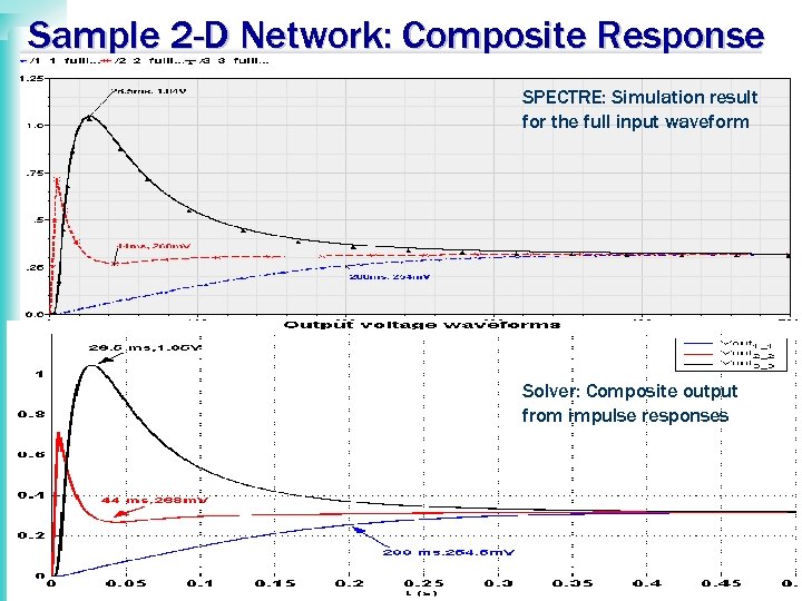
Sample 2 -D Network: Composite Response SPECTRE: Simulation result for the full input waveform Solver: Composite output from impulse responses
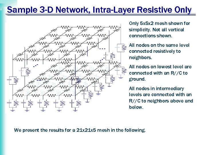
Sample 3 -D Network, Intra-Layer Resistive Only 5 x 5 x 2 mesh shown for simplicity. Not all vertical connections shown. All nodes on the same level connected resistively to neighbors. All nodes on lowest level are connected with an R//C to ground. All nodes in intermediary levels are connected with an R//C to neighbors above and below. We present the results for a 21 x 5 mesh in the following.
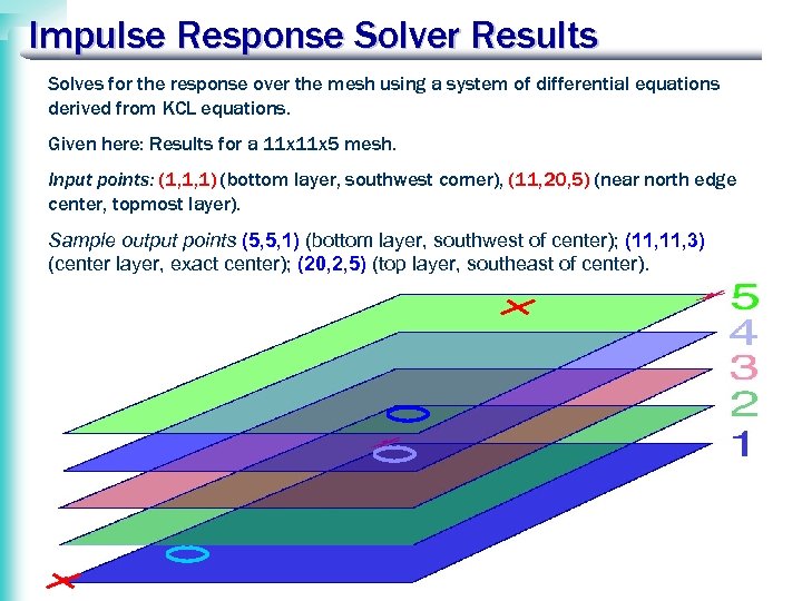
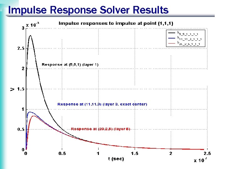
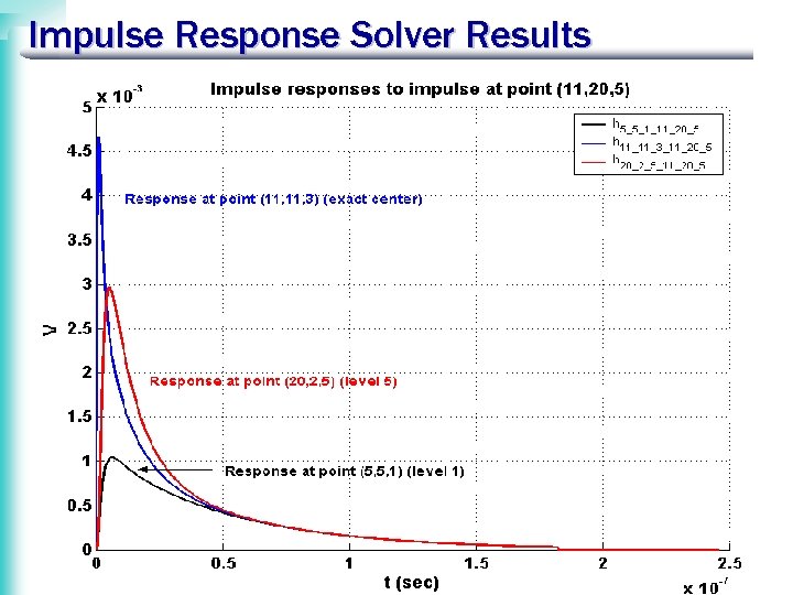
Impulse Response Solver Results Solves for the response over the mesh using a system of differential equations derived from KCL equations. Given here: Results for a 11 x 5 mesh. Input points: (1, 1, 1) (bottom layer, southwest corner), (11, 20, 5) (near north edge center, topmost layer). Sample output points (5, 5, 1) (bottom layer, southwest of center); (11, 3) (center layer, exact center); (20, 2, 5) (top layer, southeast of center).
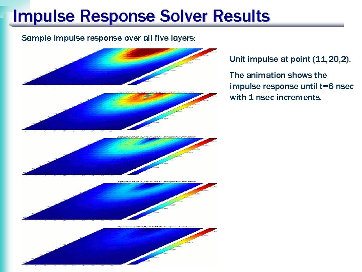
Impulse Response Solver Results Sample impulse response over all five layers: Unit impulse at point (11, 20, 2). The animation shows the impulse response until t=6 nsec with 1 nsec increments.
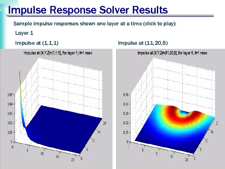
Impulse Response Solver Results Sample impulse responses shown one layer at a time (click to play): Layer 1 Impulse at (1, 1, 1) Impulse at (11, 20, 5)
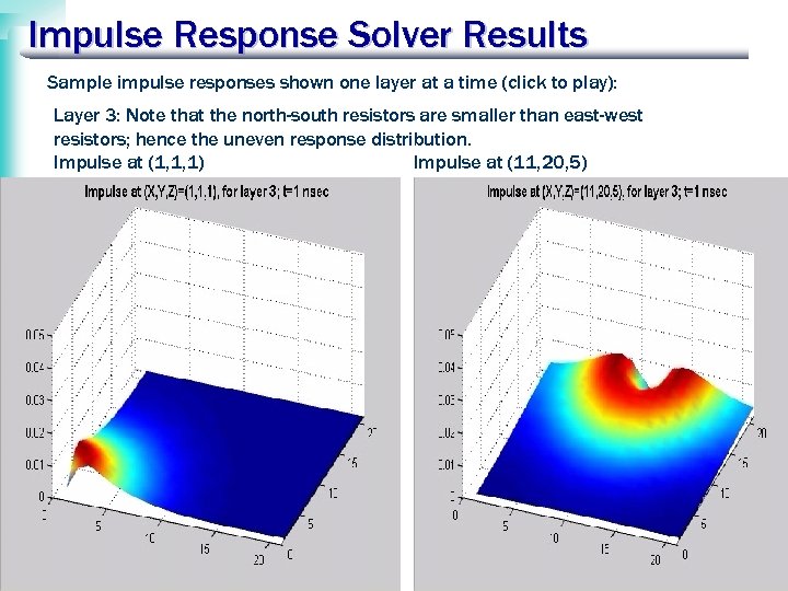
Impulse Response Solver Results Sample impulse responses shown one layer at a time (click to play): Layer 3: Note that the north-south resistors are smaller than east-west resistors; hence the uneven response distribution. Impulse at (1, 1, 1) Impulse at (11, 20, 5)
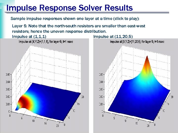
Impulse Response Solver Results Sample impulse responses shown one layer at a time (click to play): Layer 5: Note that the north-south resistors are smaller than east-west resistors; hence the uneven response distribution. Impulse at (1, 1, 1) Impulse at (11, 20, 5)
Impulse Response Solver Results
Impulse Response Solver Results
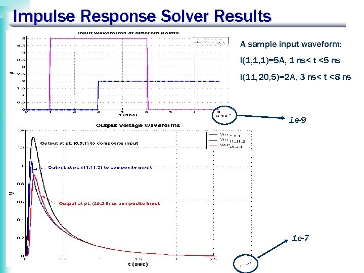
Impulse Response Solver Results A sample input waveform: I(1, 1, 1)=5 A, 1 ns< t <5 ns I(11, 20, 5)=2 A, 3 ns< t <8 ns 1 e-9 1 e-7
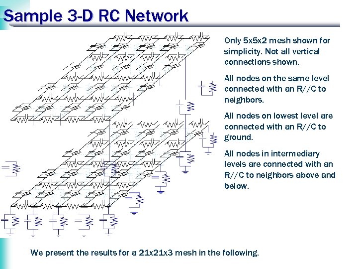
Sample 3 -D RC Network Only 5 x 5 x 2 mesh shown for simplicity. Not all vertical connections shown. All nodes on the same level connected with an R//C to neighbors. All nodes on lowest level are connected with an R//C to ground. All nodes in intermediary levels are connected with an R//C to neighbors above and below. We present the results for a 21 x 3 mesh in the following.
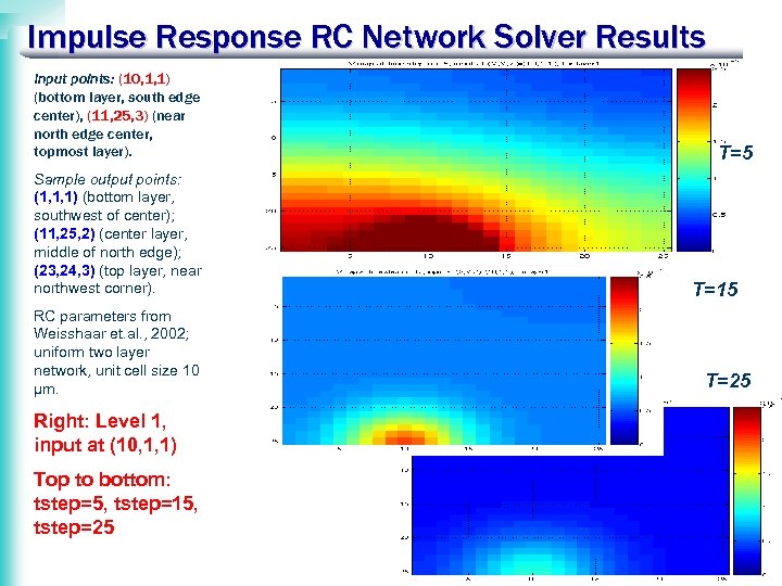
Impulse Response RC Network Solver Results Input points: (10, 1, 1) (bottom layer, south edge center), (11, 25, 3) (near north edge center, topmost layer). Sample output points: (1, 1, 1) (bottom layer, southwest of center); (11, 25, 2) (center layer, middle of north edge); (23, 24, 3) (top layer, near northwest corner). RC parameters from Weisshaar et. al. , 2002; uniform two layer network, unit cell size 10 μm. Right: Level 1, input at (10, 1, 1) Top to bottom: tstep=5, tstep=15, tstep=25 T=15 T=25
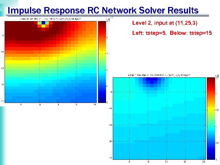
Impulse Response RC Network Solver Results Level 2, input at (11, 25, 3) Left: tstep=5, Below: tstep=15
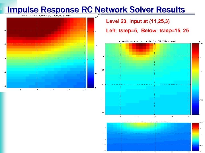
Impulse Response RC Network Solver Results Level 23, input at (11, 25, 3) Left: tstep=5, Below: tstep=15, 25
Current work • The method is flexible enough for mesh expansion; we are investigating computationally efficient ways of solving much larger mesh networks. • We are developing unit cells modeling physical interconnect structures: • On planar chips, different metal layers still form a 3 -D mesh • With appropriate unit cells, we can investigate the full networks of 3 -D integrated chips • We plan to use EM modeling tools and S-parameter measurements and extraction • Example goal application: Determine which locations are most vulnerable for substrate and ground/VDD noise-sensitive subcircuits included in 3 -D integrated system with different types of circuit networks on the individual layers (e. g. communication on top layer, data storage in the middle, data processing at the bottom…)
Conclusion • Developing a method to model and investigate the response of a complex on-chip interconnect network to external RF interference or to internal coupling between different chip regions or subcircuits. • Computational advantages: • Impulse responses calculated once yield the system response to many inputs; thus flexibility in the sources that can be examined; • Impulse responses at only the desired points in the system need to be stored to calculate the output at those points for any input waveform; • The same unit cells can be combined for many interconnect layouts; thus flexibility in the systems that can be investigated; • It is straightforward to expand the method to threedimensional networks.
9834d3c8f8e8d2ff90534baae044df2d.ppt