535e962f1b50b3a6270642094fade1f9.ppt
- Количество слайдов: 13
 An accurate and efficient SSO/SSN simulation methodology for 45 nm LPDDR I/O interface Dr. Souvik Mukherjee, Dr. Rajen Murugan (Texas Instruments Inc. ) Vinayakam Subramanian, Dr. Ji Zheng (Apache Design Solutions Inc. )
 Introduction q Needs: v Memory interface performance validation is becoming increasingly complex v Increasing speeds, design configurations, design cost optimization in die, package, board v Lower supply voltages allow for lower noise margins (due to SSO/SSN, crosstalk, ISI) on I/O performance metrics. v Look-ahead and comprehensive analysis needed during IO placement/package prototyping early analysis, signoff q Challenges: v SSO/SSN analysis is a coupled Signal-Integrity and Power-Integrity problem. v Requires concurrent modeling and simulation of the chip-package-board Signal delivery network (SDN) and power delivery network (PDN). v Combine the varying (and often conflicting) simulation requirements of the SDN and PDN. v Requires a robust and automated environment to seamlessly integrate the systemlevel model constituents. v Needs to overcome the challenge of computation complexity of traditional simulations using transistor-level model of the I/O circuits. An “ideal” SSO/SSN analysis methodology needs to accurately trade off 2 between accuracy and efficiency of modeling, extraction and simulation flows
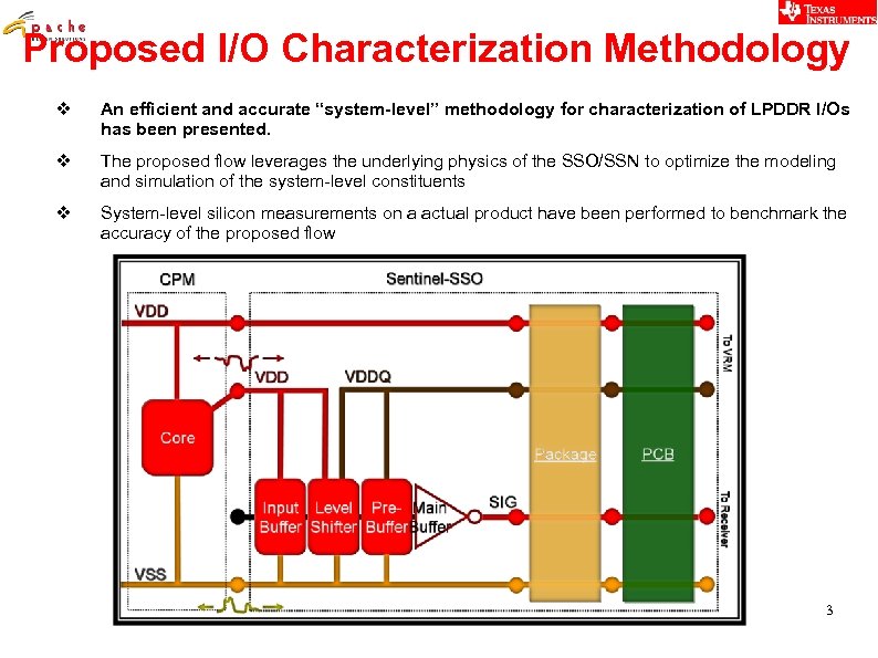 Proposed I/O Characterization Methodology v An efficient and accurate “system-level” methodology for characterization of LPDDR I/Os has been presented. v The proposed flow leverages the underlying physics of the SSO/SSN to optimize the modeling and simulation of the system-level constituents v System-level silicon measurements on a actual product have been performed to benchmark the accuracy of the proposed flow 3
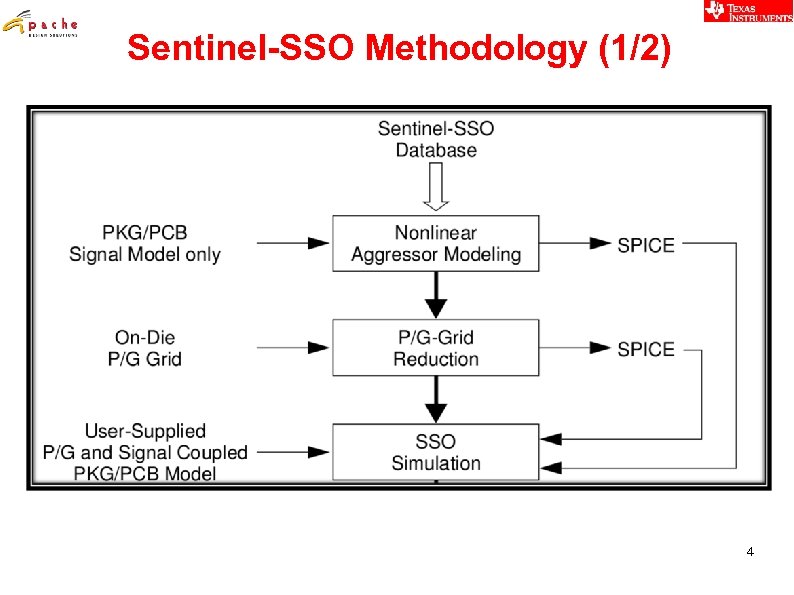 Sentinel-SSO Methodology (1/2) 4
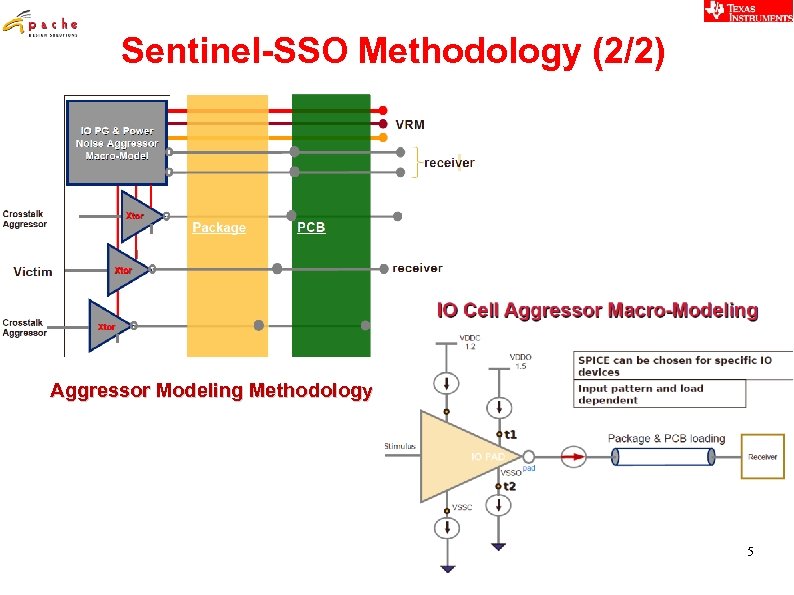 Sentinel-SSO Methodology (2/2) Aggressor Modeling Methodology 5
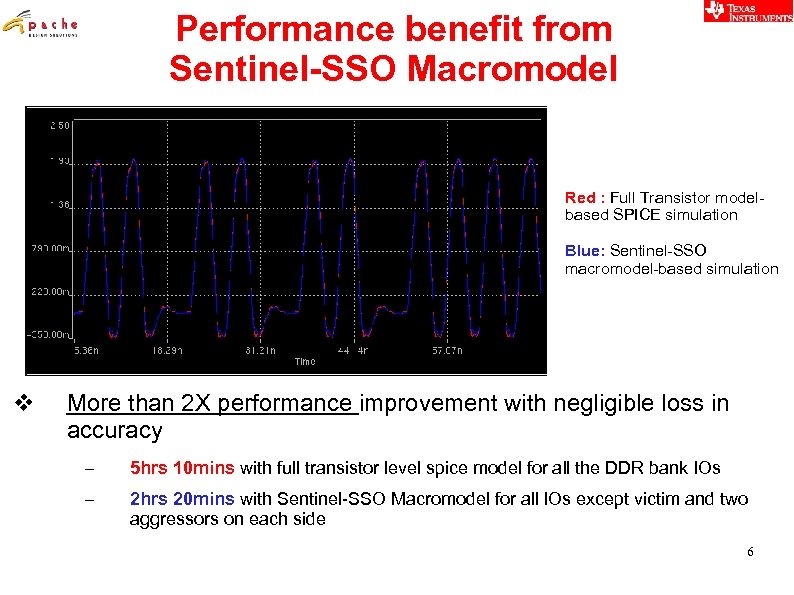 Performance benefit from Sentinel-SSO Macromodel Red : Full Transistor modelbased SPICE simulation Blue: Sentinel-SSO macromodel-based simulation v More than 2 X performance improvement with negligible loss in accuracy – 5 hrs 10 mins with full transistor level spice model for all the DDR bank IOs – 2 hrs 20 mins with Sentinel-SSO Macromodel for all IOs except victim and two aggressors on each side 6
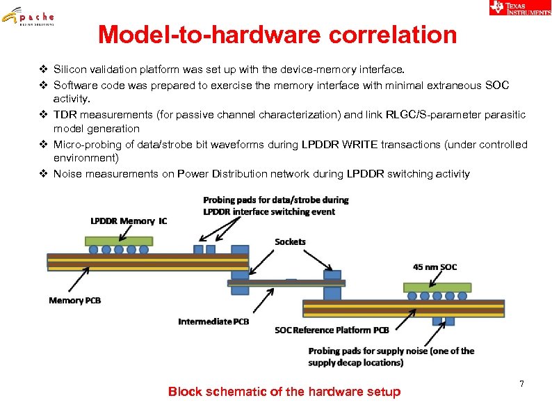 Model-to-hardware correlation v Silicon validation platform was set up with the device-memory interface. v Software code was prepared to exercise the memory interface with minimal extraneous SOC activity. v TDR measurements (for passive channel characterization) and link RLGC/S-parameter parasitic model generation v Micro-probing of data/strobe bit waveforms during LPDDR WRITE transactions (under controlled environment) v Noise measurements on Power Distribution network during LPDDR switching activity Block schematic of the hardware setup 7
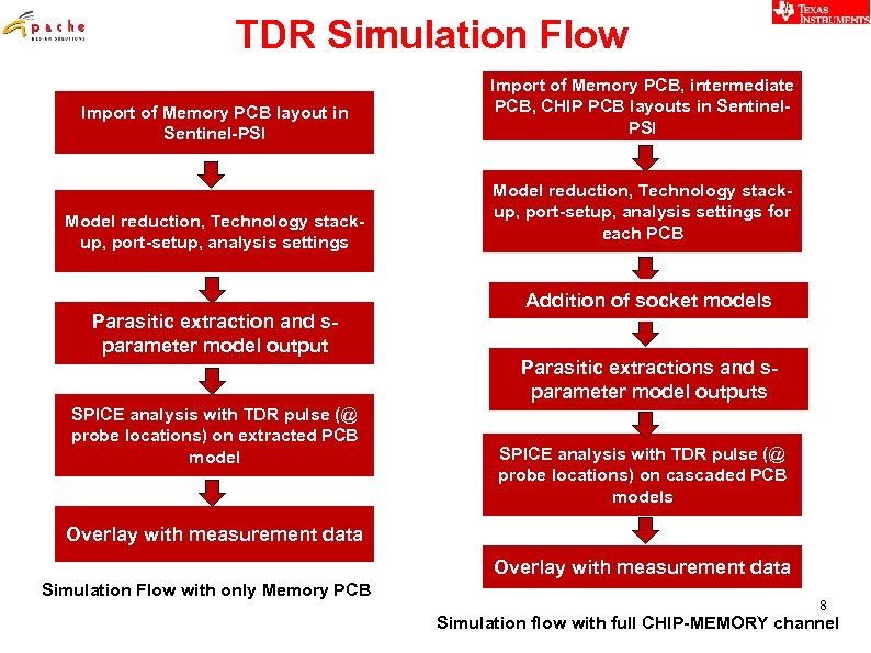 TDR Simulation Flow Import of Memory PCB layout in Sentinel-PSI Model reduction, Technology stackup, port-setup, analysis settings Parasitic extraction and sparameter model output Import of Memory PCB, intermediate PCB, CHIP PCB layouts in Sentinel. PSI Model reduction, Technology stackup, port-setup, analysis settings for each PCB Addition of socket models Parasitic extractions and sparameter model outputs SPICE analysis with TDR pulse (@ probe locations) on extracted PCB model SPICE analysis with TDR pulse (@ probe locations) on cascaded PCB models Overlay with measurement data Simulation Flow with only Memory PCB 8 Simulation flow with full CHIP-MEMORY channel
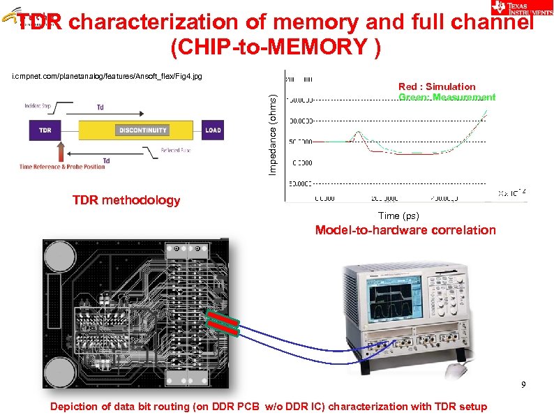 TDR characterization of memory and full channel (CHIP-to-MEMORY ) Impedance (ohms) //i. cmpnet. com/planetanalog/features/Ansoft_flex/Fig 4. jpg Red : Simulation Green: Measurement TDR methodology Time (ps) Model-to-hardware correlation 9 Depiction of data bit routing (on DDR PCB w/o DDR IC) characterization with TDR setup
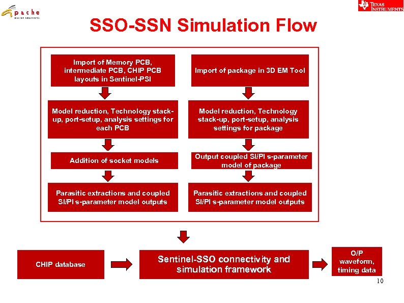 SSO-SSN Simulation Flow Import of Memory PCB, intermediate PCB, CHIP PCB layouts in Sentinel-PSI Import of package in 3 D EM Tool Model reduction, Technology stackup, port-setup, analysis settings for each PCB Model reduction, Technology stack-up, port-setup, analysis settings for package Addition of socket models Output coupled SI/PI s-parameter model of package Parasitic extractions and coupled SI/PI s-parameter model outputs CHIP database Sentinel-SSO connectivity and simulation framework O/P waveform, timing data 10
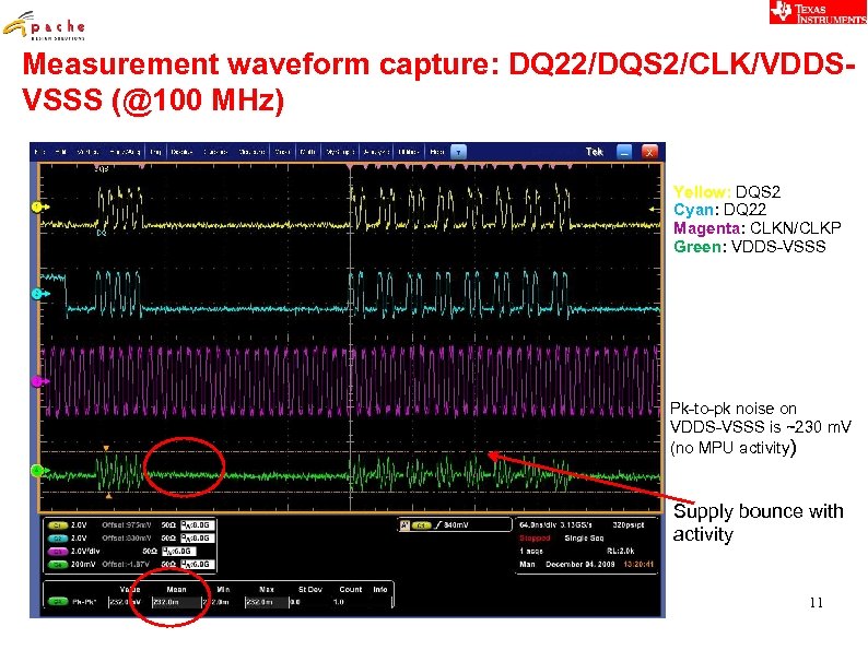 Measurement waveform capture: DQ 22/DQS 2/CLK/VDDSVSSS (@100 MHz) Yellow: DQS 2 Cyan: DQ 22 Magenta: CLKN/CLKP Green: VDDS-VSSS Pk-to-pk noise on VDDS-VSSS is ~230 m. V (no MPU activity) Supply bounce with activity 11
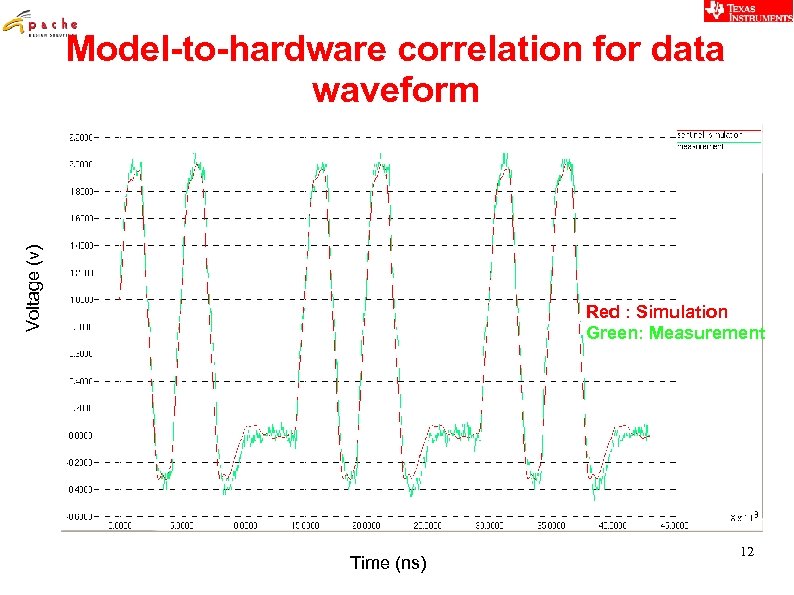 Voltage (v) Model-to-hardware correlation for data waveform Red : Simulation Green: Measurement Time (ns) 12
 Conclusions v- Develop an efficient IO macromodeling capability to analyze system-level SSO/SSN on a high-speed digital memory interface. v Demonstrated on an LPDDR memory interface for a 45 nm So. C design. v Established model-to-hardware correlation. v Innovative capability that alleviates the burden of traditional methodologies that are computationally prohibitive. 13


