339674e3319efb8634ab59342e1048fe.ppt
- Количество слайдов: 42

Advanced Semiconductor Substrates by Heterogeneous Integration Nathan Cheung Dept of EECS, UC-Berkeley cheung@eecs. berkeley. edu SOI SSOI Ge. OI 1
OUTLINE • Motivations for SOI, SSOI, and Si. Ge. OI substrates • Layer Transfer Technologies - Bonding - Delamination - Surface Smoothing • Challenges and Equipment Opportunities • Application of layer transfer for microsystem integration 2

3

Why Strain Si ? 4 Compound Semiconductor, September 2002
Why Ge. OI ? • Higher carrier mobility than that of silicon • Expected to be compatible with high-k dielectric • Dopant activation temperatures are much lower, easier to form ultra-shallow junctions. 5

Cost of Silicon Real Estate 200 mm Epi wafer 200 mm SOI or s-Si wafer $80 $0. 25/cm 2 $200 -$400 $ 0. 44 -0. 88/cm 2 1812 sq/ft House Menlo Park, CA $944, 492 $0. 56 /cm 2 6
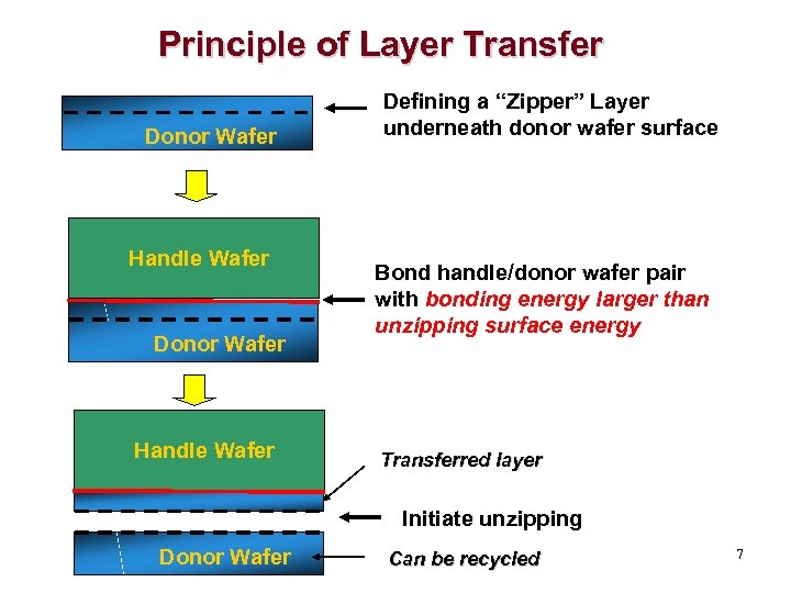
Principle of Layer Transfer Donor Wafer Handle Wafer Defining a “Zipper” Layer underneath donor wafer surface Bond handle/donor wafer pair with bonding energy larger than unzipping surface energy Transferred layer Initiate unzipping Donor Wafer Can be recycled 7
Advantages of Layer Transfer Approach • Donor wafer can be recycled • Transferred thickness and buried oxide thickness are independently controlled • Lower processing temperature than SIMOX approach • Multi-stack structures can be achieved • Silicon-on-Anything (SOA) composite substrates 8

Direct Wafer Bonding Chemical Cleaning: HF, H 2 SO 4, H 2 O 2 IR Transmission Image Through a Bonded Pair Plasma exposure Room temperature bonding Annealing Complete bonding over 4 inch diameter 9
![Delamination Methods (1) Exfoliation of implanted hydrogen [ SOITEC, Amberwave] Si donor Transferred Si Delamination Methods (1) Exfoliation of implanted hydrogen [ SOITEC, Amberwave] Si donor Transferred Si](https://present5.com/presentation/339674e3319efb8634ab59342e1048fe/image-10.jpg)
Delamination Methods (1) Exfoliation of implanted hydrogen [ SOITEC, Amberwave] Si donor Transferred Si overlayer Handle wafer (2) Cleavage along implant damage region (gas jet) [Sigen] (3) Mechanical rupture of Porous Si (water jet) [Canon] 10
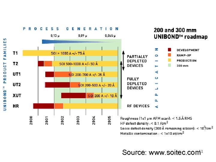
11 Source: www. soitec. com

Requirements for Direct Bonding ØSurface micro-roughness ~ nm ØNo macroscopic wafer warpage ØMinimal particle density and size - 1 um particle will give 1000 um void ØContamination free surface 12

Weak Van der Waals : < 20 m. J/m 2 H-bonding : < 500 m. J/m 2 Covalent bonding: > 2000 m. J/m 2 Strong 13

Hydrophilic Bonding Model O O * *Si * O Si O O Si H H H 2 O H Si O H O O Si O O H H O H Si H As prepared O H H O Si O O Room temp bonding O Si H O O < 100 o. C O H Si O H 2 O O Si Si O O Si-OH + Si-OH ---> Si-O-Si + H 2 O Si + 2 H 2 O ---> Si. O 2 + 2 H 2 > 100 o. C 14
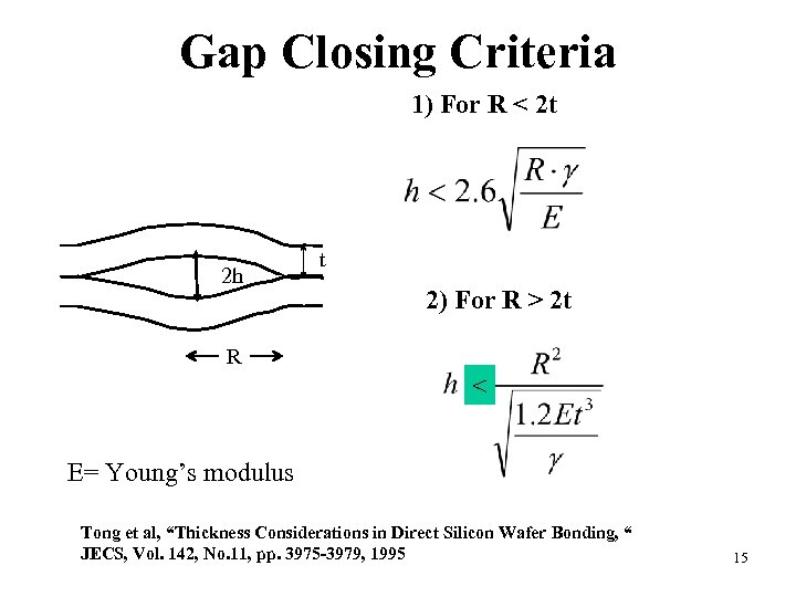
Gap Closing Criteria 1) For R < 2 t 2 h t 2) For R > 2 t R < E= Young’s modulus Tong et al, “Thickness Considerations in Direct Silicon Wafer Bonding, “ JECS, Vol. 142, No. 11, pp. 3975 -3979, 1995 15
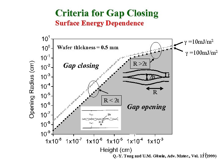
Criteria for Gap Closing Surface Energy Dependence =10 m. J/m 2 Wafer thickness = 0. 5 mm =100 m. J/m 2 R >2 t Gap closing 2 h t R R < 2 t Gap opening 16 Q. -Y. Tong and U. M. Gösele, Adv. Mater. , Vol. 11 (1999)
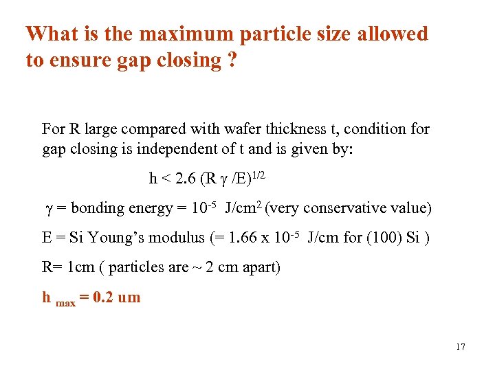
What is the maximum particle size allowed to ensure gap closing ? For R large compared with wafer thickness t, condition for gap closing is independent of t and is given by: h < 2. 6 (R /E)1/2 = bonding energy = 10 -5 J/cm 2 (very conservative value) E = Si Young’s modulus (= 1. 66 x 10 -5 J/cm for (100) Si ) R= 1 cm ( particles are ~ 2 cm apart) h max = 0. 2 um 17
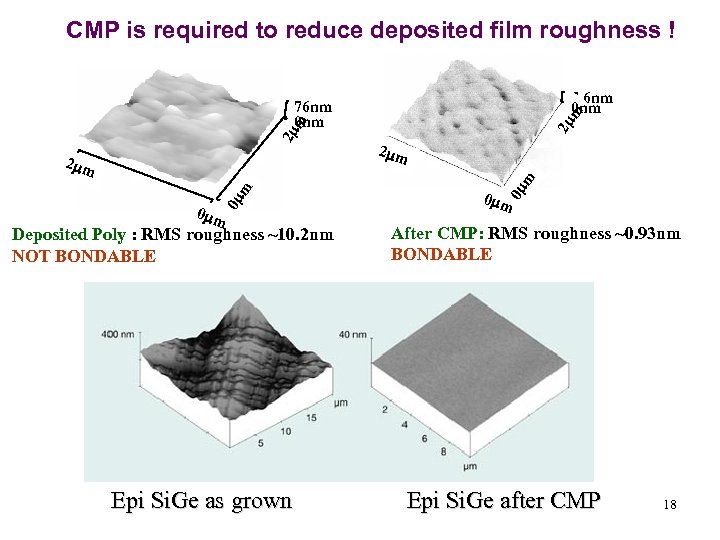
CMP is required to reduce deposited film roughness ! 7. 6 nm 0 m m 2 mm 0 mm Deposited Poly : RMS roughness ~10. 2 nm NOT BONDABLE Epi Si. Ge as grown 2 m m 2 mm 0 m m 2 m m 76 nm 0 mm After CMP: RMS roughness ~0. 93 nm BONDABLE Epi Si. Ge after CMP 18
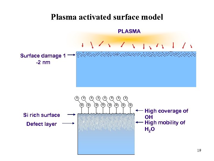
Plasma activated surface model PLASMA Surface damage 1 -2 nm H H O Si rich surface Defect layer H O H O H H O O High coverage of OH High mobility of H 2 O 19
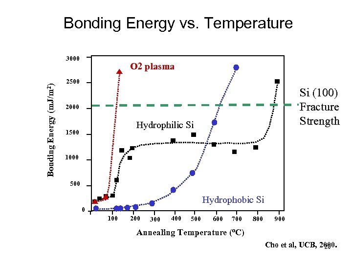
Bonding Energy vs. Temperature Bonding Energy (m. J/m 2) 3000 O 2 plasma 2500 Si (100) Fracture Strength 2000 Hydrophilic Si 1500 1000 500 Hydrophobic Si 0 100 200 300 400 500 600 700 800 900 Annealing Temperature (o. C) Cho et al, UCB, 2000. 20
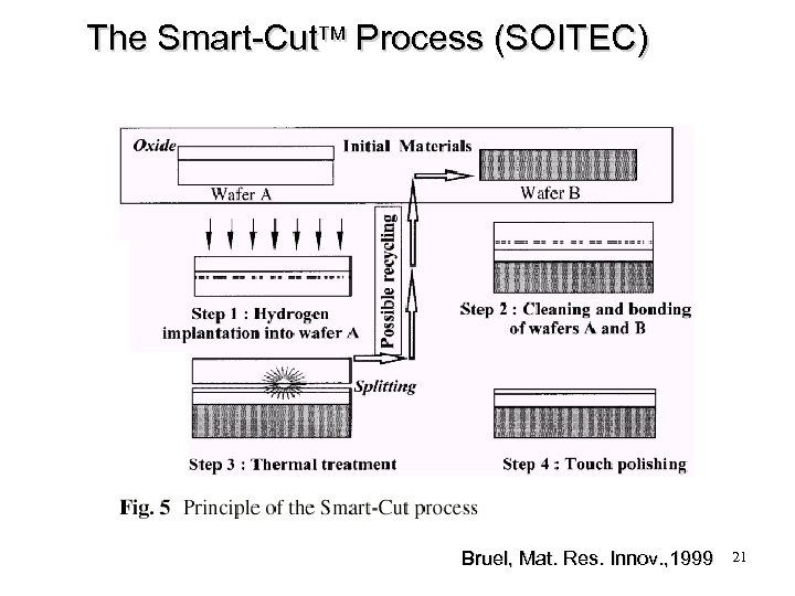
The Smart-Cut Process (SOITEC) Bruel, Mat. Res. Innov. , 1999 21
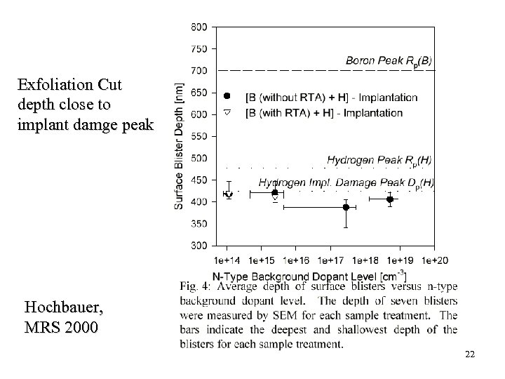
Exfoliation Cut depth close to implant damge peak Hochbauer, MRS 2000 22

The Nanocleave. TM Process (Si. Gen) DONOR RECLAIM / SURFACE FINISH DONOR OXIDIZE AND CLEAVE PLANE FORMATION NEW HANDLE BOND Key Process Steps • Epitaxial deposition • Implantation • Oxidation • Plasma activation and bonding • Layer transfer and cleaving • Epitaxial smoothing and thickening r. T-CCP™ EPI-Smooth/Thicken Malik et al, Semicon Europa, 2003 23

“Cold-Cut” : Edge Initiated Mechanical Cleavage • Razor Blade • Water Jet • Gas Blade Stress Concentration at Crack Tips Length of the crack = 2 a Radius of curvature at tip = C 2 a Applied Stress = Stress at crack-tip = C 24
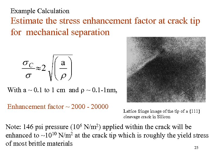
Example Calculation Estimate the stress enhancement factor at crack tip for mechanical separation With a ~ 0. 1 to 1 cm and ~ 0. 1 -1 nm, Enhancement factor ~ 2000 - 20000 Lattice fringe image of the tip of a {111} cleavage crack in Silicon Note: 146 psi pressure (106 N/m 2) applied within the crack will be enhanced to ~1010 N/m 2 at the crack tip which is roughly the yield stress of most brittle materials 25

Nano. Cleave rms ~ 0. 8 nm Hydrogen Induced Thermal Separation rms ~ 8. 5 nm Current et al, European Semiconductor, Feb 2000 26
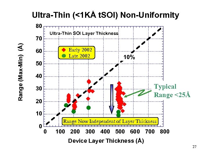
Ultra-Thin (<1 KÅ t. SOI) Non-Uniformity 80 Ultra-Thin SOI Layer Thickness Range (Max-Min) (Å) 70 Early 2002 Late 2002 60 10% 50 40 Typical Range <25Å 30 20 10 0 Range Now Independent of Layer Thickness 0 100 200 300 400 500 600 700 800 Device Layer Thickness (Å) 27
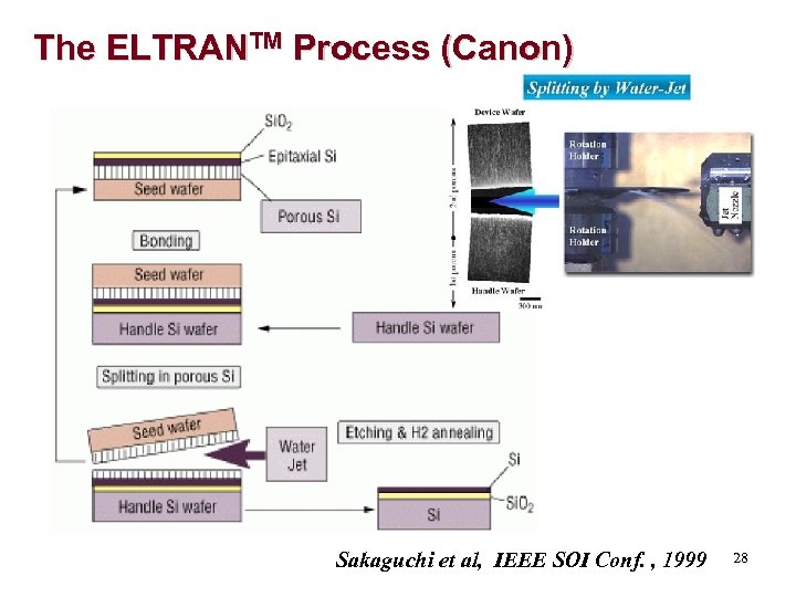
The ELTRANTM Process (Canon) Sakaguchi et al, IEEE SOI Conf. , 1999 28

As-split surface After-anneal surface Smoothing by Hydrogen anneal 29
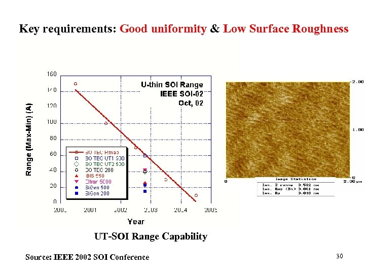
Key requirements: Good uniformity & Low Surface Roughness UT-SOI Range Capability Source: IEEE 2002 SOI Conference 30
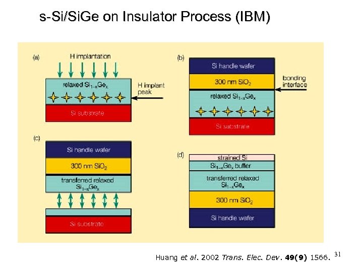
s-Si/Si. Ge on Insulator Process (IBM) Huang et al. 2002 Trans. Elec. Dev. 49(9) 1566. 31

32 G. Cellar, SOITEC Technical Notes, 2003

Relaxed Si. Ge surface roughness can be reduced Malik et al, Semicon Europa, 2003 33
FLCC Research : Uniformity and Roughness Control • Low-temperature plasma surface treatment to improve bonding strength between Si. O 2 and Si. Ge • Other ways to enhance bonding strength (photons, ions, vapor) • Modeling and verification of thermal, implant, and bonding stress effects on transferred thickness and roughness 34

Plasma Assisted Bonding for SGOI EXP. Set-up IR Camera Si-Ge bonding strength IR Lamp Refractive Infrared Imaging Si or Si. O 2 Ge Image: Si-Ge pair Non-bonded Area Bottom Ge Top Si WC 1 WC 2 O 2 plasma WC 3 35
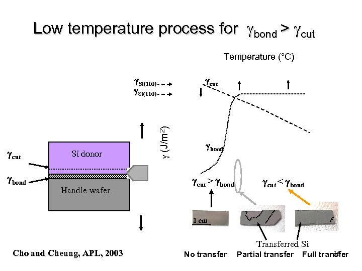
Low temperature process for bond > cut Temperature (°C) g. Si(100) g. Si(110) gbond Handle wafer (J/m 2) gcut Si donor gcut gbond gcut > gbond gcut < gbond 1 cm Cho and Cheung, APL, 2003 Transferred Si No transfer Partial transfer 36 Full transfer
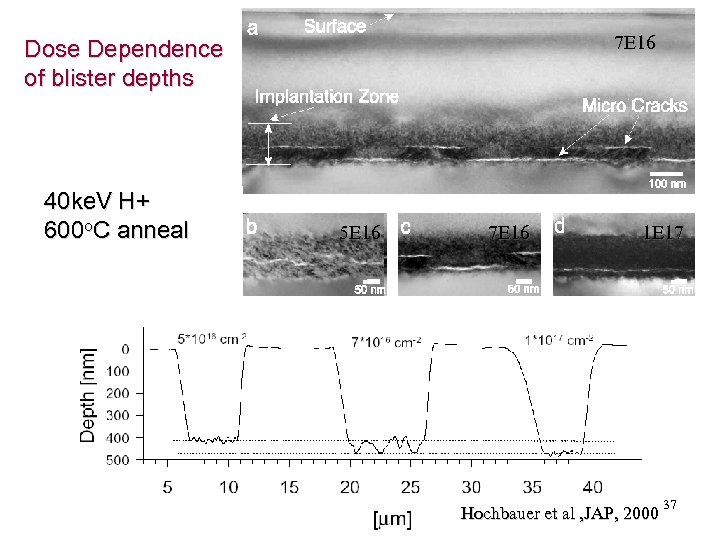
7 E 16 Dose Dependence of blister depths 40 ke. V H+ 600 o. C anneal 5 E 16 7 E 16 1 E 17 Hochbauer et al , JAP, 2000 37

Manufacturing Equipment Opportunities • High-throughput, low-cost Epi Reactors • CMP of Si. Ge and Strained Si • High Current Hydrogen implanters • Plasma Activated Bonders • Mechanical Delamination Machines Plasma Bonder Gas Jet Delamination H+ Plasma Implanter 38

Zero-footprint optical metrology wafer Data transmission/ Dielectric layer diagnostics MEMS Sensor Si Photon emitter Data processing, Li-polymer Detector Photon emitter storage unit Battery § Self-powered diagnostic and monitoring wafer § Deposition/etching uniformity and CMP end-point mapping. §Work in hostile processing environments ( Plasma, wet etching, CMP). § 1% thickness resolution is achievable. 39 www. sfr. berkeley. edu

Heterogeneous Integration of Ga. N LED, Cd. Se optical filter , Si detector, and microfluidic channels LED Cd. S 0. 9 Se 0. 1 filter Cd. S filter 5 mm Green LED Blue LED 5 mm Packaged prototype XYZ chip. Light sources: Blue (463 nm) and green (525 nm) (In, Ga)N LEDs were used to excite yellow-green (494/518) and red-orange (565/580) Fluo. Spheres® carboxylate-modified microspheres ( 0. 04 µm in size)*, respectively. Filters: Cd. S (1. 1 m) and Cd. S 0. 9 Se 0. 1 (1. 1 m) filter were used to filter out the emission light for blue and green LEDs, respectively. Fluidic channel: PDMS (polydimenthyl siloxane) channel: 2 mm wide, 100 m deep and 7 mm long. 40
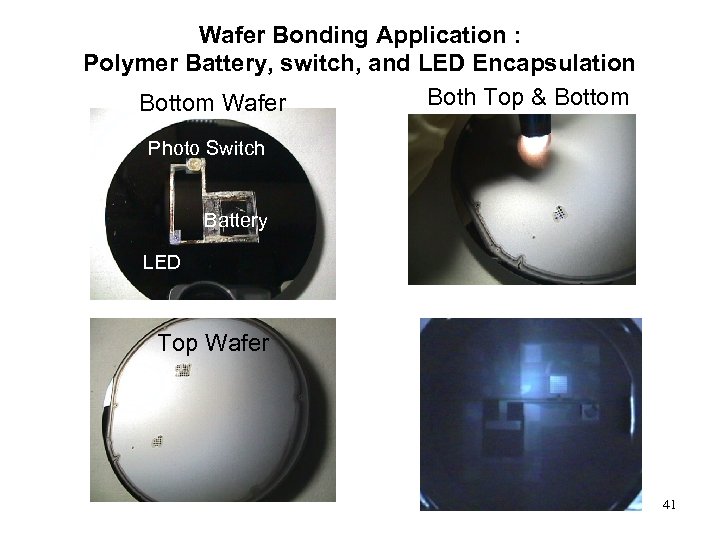
Wafer Bonding Application : Polymer Battery, switch, and LED Encapsulation Both Top & Bottom Wafer Photo Switch Battery LED Top Wafer 41
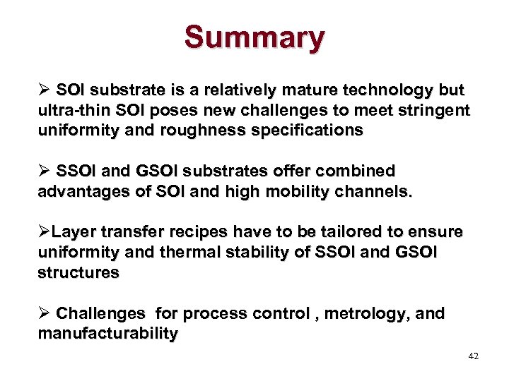
Summary Ø SOI substrate is a relatively mature technology but ultra-thin SOI poses new challenges to meet stringent uniformity and roughness specifications Ø SSOI and GSOI substrates offer combined advantages of SOI and high mobility channels. ØLayer transfer recipes have to be tailored to ensure uniformity and thermal stability of SSOI and GSOI structures Ø Challenges for process control , metrology, and manufacturability 42
339674e3319efb8634ab59342e1048fe.ppt