1294cfea351fb41a02b60a22d0d7d845.ppt
- Количество слайдов: 32
 Administration • Midterm on Thursday Oct 28. Covers material through 10/21. • Histogram of grades for HW#1 posted on newsgroup. • Sample problem set (and solutions) on pipelining are posted on the web page. • Last year’s practice exam, and last year’s midterm (with solutions) are on web site (under “Exams”) CIS 501, Fall 99 MBG 1
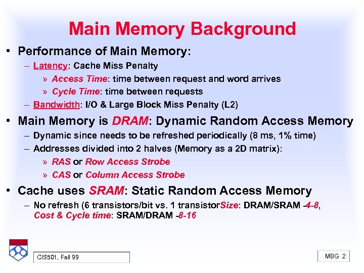 Main Memory Background • Performance of Main Memory: – Latency: Cache Miss Penalty » Access Time: time between request and word arrives » Cycle Time: time between requests – Bandwidth: I/O & Large Block Miss Penalty (L 2) • Main Memory is DRAM: Dynamic Random Access Memory – Dynamic since needs to be refreshed periodically (8 ms, 1% time) – Addresses divided into 2 halves (Memory as a 2 D matrix): » RAS or Row Access Strobe » CAS or Column Access Strobe • Cache uses SRAM: Static Random Access Memory – No refresh (6 transistors/bit vs. 1 transistor. Size: DRAM/SRAM 4 -8, Cost & Cycle time: SRAM/DRAM 8 -16 CIS 501, Fall 99 MBG 2
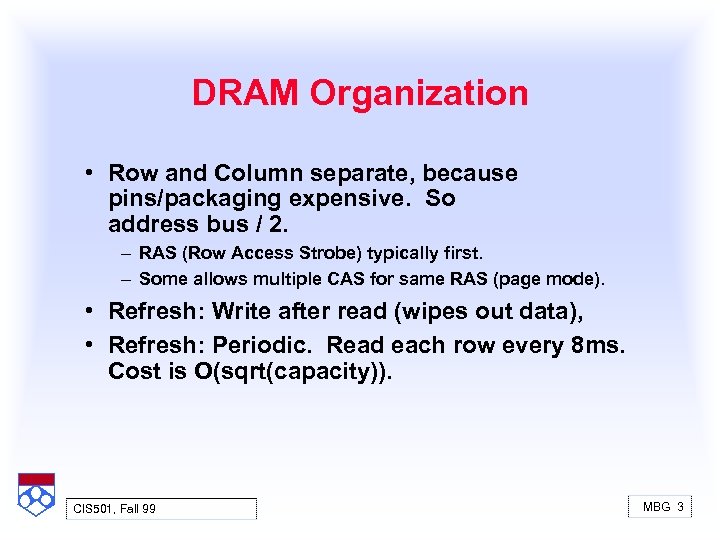 DRAM Organization • Row and Column separate, because pins/packaging expensive. So address bus / 2. – RAS (Row Access Strobe) typically first. – Some allows multiple CAS for same RAS (page mode). • Refresh: Write after read (wipes out data), • Refresh: Periodic. Read each row every 8 ms. Cost is O(sqrt(capacity)). CIS 501, Fall 99 MBG 3
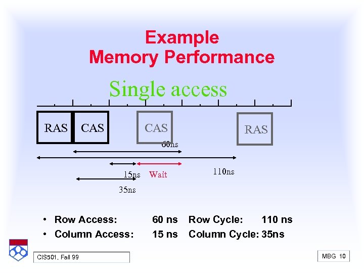
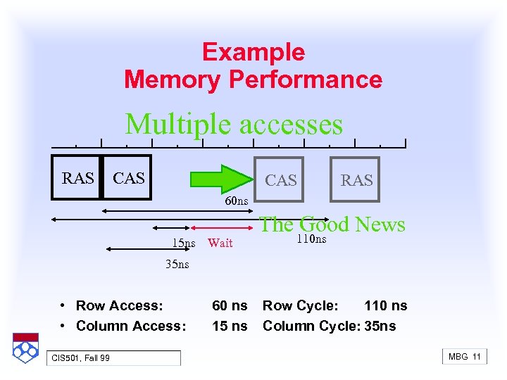
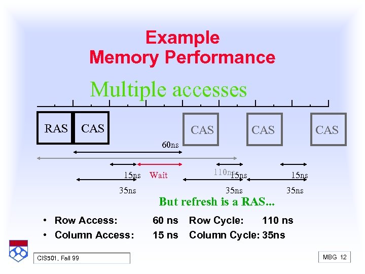
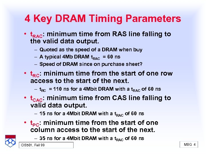 4 Key DRAM Timing Parameters • t. RAC: minimum time from RAS line falling to the valid data output. – Quoted as the speed of a DRAM when buy – A typical 4 Mb DRAM t. RAC = 60 ns – Speed of DRAM since on purchase sheet? • t. RC: minimum time from the start of one row access to the start of the next. – t. RC = 110 ns for a 4 Mbit DRAM with a t. RAC of 60 ns • t. CAC: minimum time from CAS line falling to valid data output. – 15 ns for a 4 Mbit DRAM with a t. RAC of 60 ns • t. PC: minimum time from the start of one column access to the start of the next. – 35 ns for a 4 Mbit DRAM with a t. RAC of 60 ns CIS 501, Fall 99 MBG 4
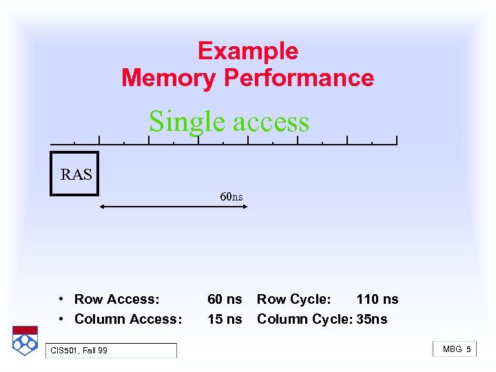 Example Memory Performance Single access RAS 60 ns • Row Access: • Column Access: CIS 501, Fall 99 60 ns 15 ns Row Cycle: 110 ns Column Cycle: 35 ns MBG 5
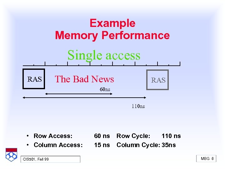 Example Memory Performance Single access RAS The Bad News RAS 60 ns 110 ns • Row Access: • Column Access: CIS 501, Fall 99 60 ns 15 ns Row Cycle: 110 ns Column Cycle: 35 ns MBG 6
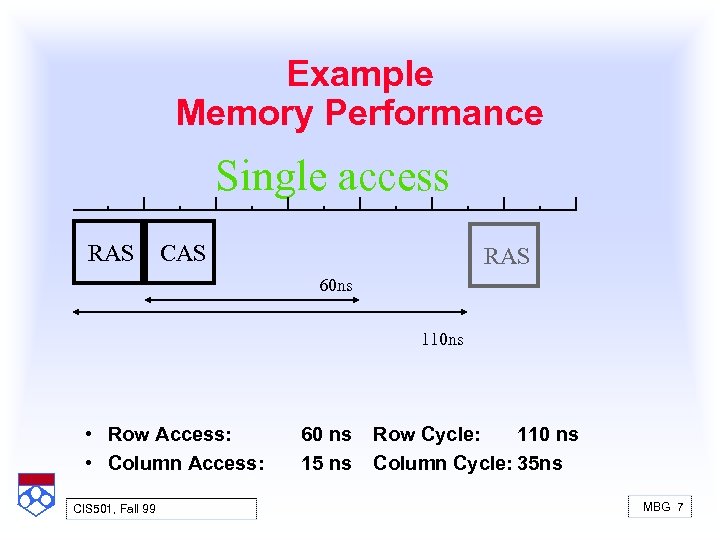 Example Memory Performance Single access RAS CAS RAS 60 ns 110 ns • Row Access: • Column Access: CIS 501, Fall 99 60 ns 15 ns Row Cycle: 110 ns Column Cycle: 35 ns MBG 7
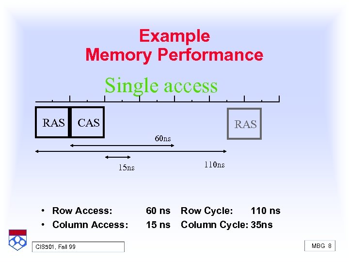 Example Memory Performance Single access RAS CAS RAS 60 ns 110 ns 15 ns • Row Access: • Column Access: CIS 501, Fall 99 60 ns 15 ns Row Cycle: 110 ns Column Cycle: 35 ns MBG 8
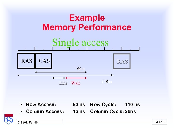 Example Memory Performance Single access RAS CAS RAS 60 ns 15 ns Wait • Row Access: • Column Access: CIS 501, Fall 99 60 ns 15 ns 110 ns Row Cycle: 110 ns Column Cycle: 35 ns MBG 9
 Example Memory Performance Single access RAS CAS RAS 60 ns 15 ns Wait 110 ns 35 ns • Row Access: • Column Access: CIS 501, Fall 99 60 ns 15 ns Row Cycle: 110 ns Column Cycle: 35 ns MBG 10
 Example Memory Performance Multiple accesses RAS CAS RAS 60 ns 15 ns Wait The Good News 110 ns 35 ns • Row Access: • Column Access: CIS 501, Fall 99 60 ns 15 ns Row Cycle: 110 ns Column Cycle: 35 ns MBG 11
 Example Memory Performance Multiple accesses RAS CAS CAS 60 ns 15 ns Wait 35 ns • Row Access: • Column Access: CIS 501, Fall 99 110 ns 15 ns 35 ns But refresh is a RAS. . . 60 ns 15 ns 35 ns Row Cycle: 110 ns Column Cycle: 35 ns MBG 12
 DRAM Performance • A 60 ns (t. RAC) DRAM can – perform a row access only every 110 ns (t. RC) – perform column access (t. CAC) in 15 ns, but time between column accesses is at least 35 ns (t. PC). » In practice, external address delays and turning around buses make it 40 to 50 ns • These times do not include the time to drive the addresses off the microprocessor nor the memory controller overhead! CIS 501, Fall 99 MBG 13
 DRAM Trends • DRAMs: capacity +60%/yr, cost – 30%/yr – 2. 5 X cells/area, 1. 5 X die size in _3 years • ‘ 98 DRAM fab line costs $2 B • Commodity, second source industry => high volume, low profit, conservative • Order of importance: 1) Cost/bit 2) Capacity – First RAMBUS: 10 X BW, +30% cost => little impact – Gigabit DRAM will take over market CIS 501, Fall 99 MBG 14
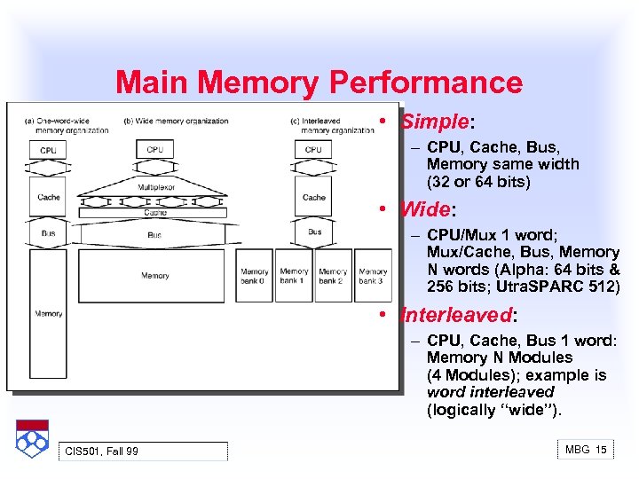 Main Memory Performance • Simple: – CPU, Cache, Bus, Memory same width (32 or 64 bits) • Wide: – CPU/Mux 1 word; Mux/Cache, Bus, Memory N words (Alpha: 64 bits & 256 bits; Utra. SPARC 512) • Interleaved: – CPU, Cache, Bus 1 word: Memory N Modules (4 Modules); example is word interleaved (logically “wide”). CIS 501, Fall 99 MBG 15
 Why not have wider memory? • Pins, packaging • CPU accesses word at a time. Need multiplexer in critical path. • Unit of expansion. • ECC (need to read full ECC block on every write to portion of block). CIS 501, Fall 99 MBG 16
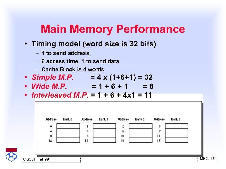 Main Memory Performance • Timing model (word size is 32 bits) – 1 to send address, – 6 access time, 1 to send data – Cache Block is 4 words • Simple M. P. = 4 x (1+6+1) = 32 • Wide M. P. =1+6+1 =8 • Interleaved M. P. = 1 + 6 + 4 x 1 = 11 CIS 501, Fall 99 MBG 17
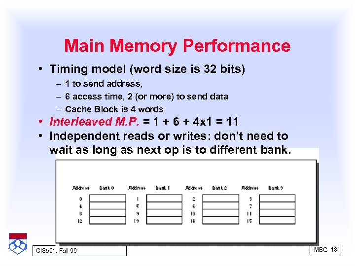 Main Memory Performance • Timing model (word size is 32 bits) – 1 to send address, – 6 access time, 2 (or more) to send data – Cache Block is 4 words • Interleaved M. P. = 1 + 6 + 4 x 1 = 11 • Independent reads or writes: don’t need to wait as long as next op is to different bank. CIS 501, Fall 99 MBG 18
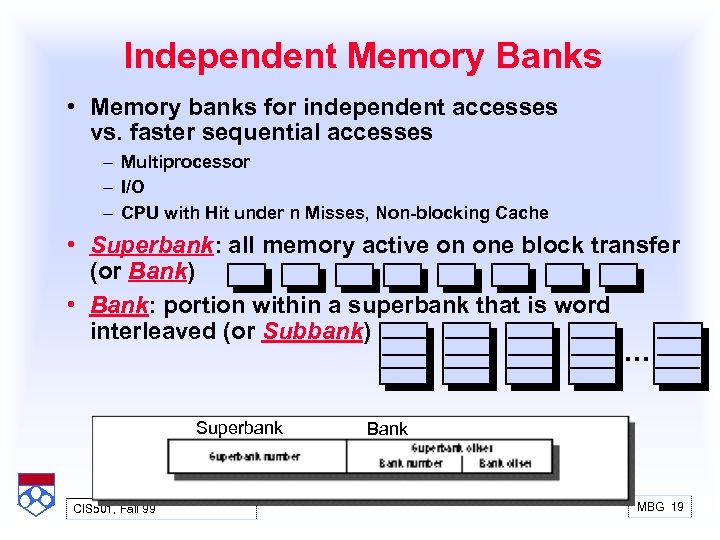 Independent Memory Banks • Memory banks for independent accesses vs. faster sequential accesses – Multiprocessor – I/O – CPU with Hit under n Misses, Non blocking Cache • Superbank: all memory active on one block transfer (or Bank) • Bank: portion within a superbank that is word interleaved (or Subbank) … Superbank CIS 501, Fall 99 Bank MBG 19
 Independent Memory Banks • How many banks? number banks >= number clocks to access word in bank – For sequential accesses, otherwise will return to original bank before it has next word ready • Increasing DRAM => fewer chips => harder to have banks CIS 501, Fall 99 MBG 20
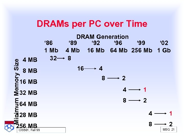 Minimum Memory Size DRAMs per PC over Time 4 MB 8 MB 16 MB 32 MB 64 MB ‘ 86 1 Mb 32 DRAM Generation ‘ 89 ‘ 92 ‘ 96 ‘ 99 ‘ 02 4 Mb 16 Mb 64 Mb 256 Mb 1 Gb 8 16 4 8 2 4 1 8 2 128 MB 4 1 256 MB 8 2 CIS 501, Fall 99 MBG 21
 Fast Memory Systems: DRAM specific • Multiple CAS accesses: several names (page mode) – Extended Data Out (EDO): 30% faster in page mode • New DRAMs to address gap; – RAMBUS: reinvent DRAM interface » Each Chip a module vs. slice of memory » Short bus between CPU and chips » Does own refresh » Variable amount of data returned » 1 byte / 2 ns (500 MB/s per chip) – Synchronous DRAM: 2 banks on chip, a clock signal to DRAM, transfer synchronous to system clock (66 150 MHz) • RAMBUS first seen as niche (e. g. video memory), now poised to become standard. CIS 501, Fall 99 MBG 22
 Main Memory Organization DRAM/Disk interface CIS 501, Fall 99 MBG 23
 Four Questions for Memory Hierarchy Designers • Q 1: Where can a block be placed in the upper level? (Block placement) • Q 2: How is a block found if it is in the upper level? (Block identification) • Q 3: Which block should be replaced on a miss? (Block replacement) • Q 4: What happens on a write? (Write strategy) CIS 501, Fall 99 MBG 24
 Four Questions Applied to Virtual Memory • Q 1: Where can a block be placed in the upper level? (Block placement: fully-associative vs. page coloring) • Q 2: How is a block found if it is in the upper level? (Block identification: translation & lookup, pagetables and TLB) • Q 3: Which block should be replaced on a miss? (Block replacement: random vs. LRU) • Q 4: What happens on a write? (Write strategy: copy-on-write, protection, etc. ) • Q? : protection? demand load vs. prefetch? fixed vs. variable size? unit of transfer vs. frame size. Software CIS 501, Fall 99 MBG 25
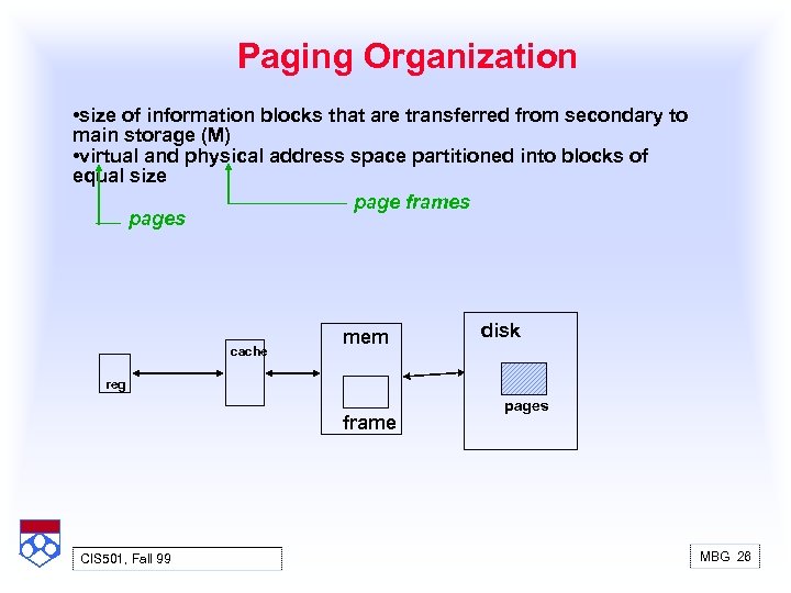 Paging Organization • size of information blocks that are transferred from secondary to main storage (M) • virtual and physical address space partitioned into blocks of equal size page frames pages cache mem disk reg frame CIS 501, Fall 99 pages MBG 26
 Addresses in Virtual Memory • 3 addresses to consider – Physical address: where in main memory frame is stored – Virtual address: a logical address, relative to process/name space/page table – Disk address: specifying where on disk page is stored. • Disk addresses can be either physical (specifying cyclinder, block, etc. ) or indirect (another level of naming even file system or segment). • Virtual addresses logically include a process_id concatenated to n bit address. CIS 501, Fall 99 MBG 27
 Virtual Address Space and Physical Address Space sizes • From point of view of hierarchy, the disk will have more capacity than DRAM BUT, this does not mean that virtual address space will be bigger than physical address space. • Virtual addresses provide protection and a naming mechanism. • A long, time ago, some machines had physical address space bigger than virtual address space, and more core than vaddr space. (Multiple processes in memory at same time). CIS 501, Fall 99 MBG 28
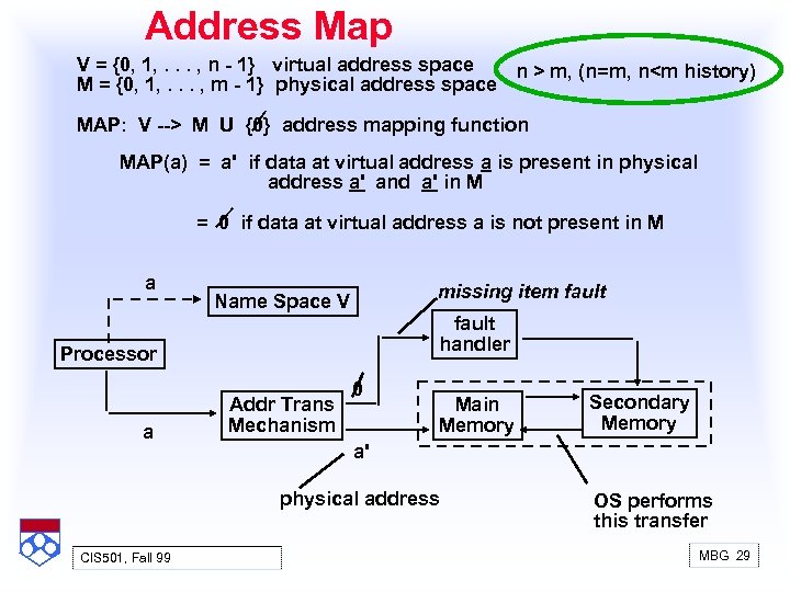 Address Map V = {0, 1, . . . , n 1} virtual address space n > m, (n=m, n
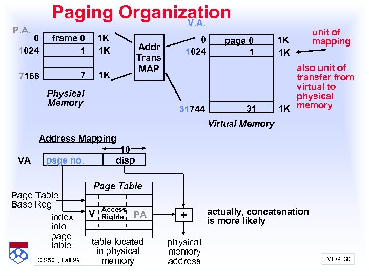 Paging Organization V. A. P. A. 0 1024 frame 0 1 1 K 1 K 7 7168 Addr Trans MAP 1 K Physical Memory 0 1024 31744 page 0 1 31 1 K 1 K unit of mapping also unit of transfer from virtual to physical 1 K memory Virtual Memory Address Mapping VA 10 disp page no. Page Table Base Reg index into page table CIS 501, Fall 99 Page Table V Access Rights PA table located in physical memory + physical memory address actually, concatenation is more likely MBG 30
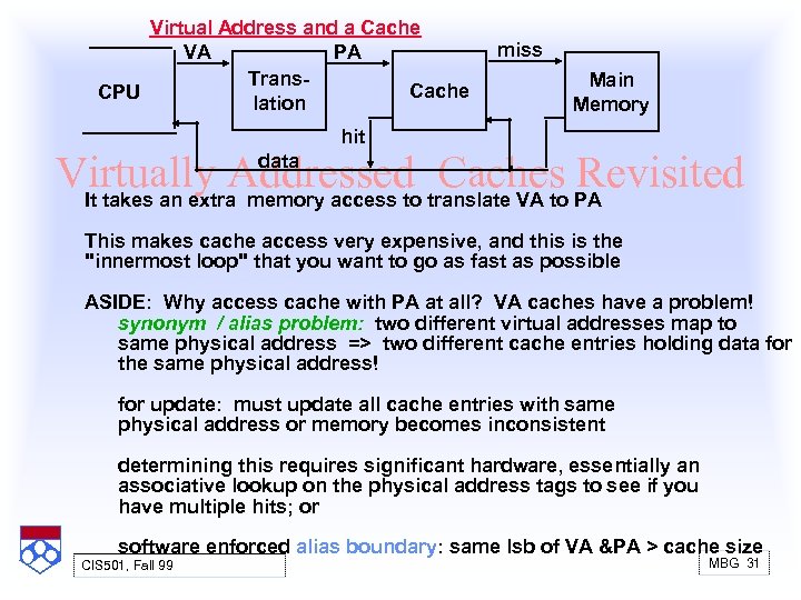 Virtual Address and a Cache VA PA Trans Cache CPU lation miss Main Memory hit Virtually Addressed translate VA to PA Caches Revisited It takes an extra memory access to data This makes cache access very expensive, and this is the "innermost loop" that you want to go as fast as possible ASIDE: Why access cache with PA at all? VA caches have a problem! synonym / alias problem: two different virtual addresses map to same physical address => two different cache entries holding data for the same physical address! for update: must update all cache entries with same physical address or memory becomes inconsistent determining this requires significant hardware, essentially an associative lookup on the physical address tags to see if you have multiple hits; or software enforced alias boundary: same lsb of VA &PA > cache size CIS 501, Fall 99 MBG 31
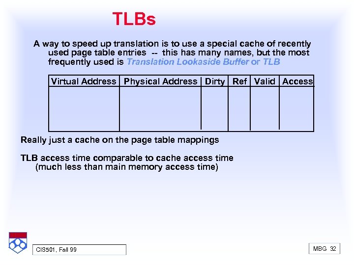 TLBs A way to speed up translation is to use a special cache of recently used page table entries this has many names, but the most frequently used is Translation Lookaside Buffer or TLB Virtual Address Physical Address Dirty Ref Valid Access Really just a cache on the page table mappings TLB access time comparable to cache access time (much less than main memory access time) CIS 501, Fall 99 MBG 32


