9016cefc75c56bc1fd553819d66094ee.ppt
- Количество слайдов: 34
Adaptive System on a Chip (ASOC): A Backbone for Power-Aware Signal Processing Cores Andrew Laffely, Jian Liang, Russ Tessier and Wayne Burleson Electrical and Computer Engineering University of Massachusetts Amherst {burleson}@ecs. umass. edu This material is based upon work supported by the National Science Foundation under Grant No. 9988238 and SRC Tasks 766 and 1075 Burleson, UMASS 1
Challenges in Media Processing • Increasingly complex, heterogeneous algorithms Variable run-times (e. g. data-dependent iterations) • Variable quality • Variable power consumption • • Large data-sets, usually streaming • • Memory size, ports and latency issues Advancing semiconductor technology (Moore’s Law) Interconnect (on-chip and I/O) • Clocking • Power (consumption and distribution) • Design and Verification • Burleson/UMASS 2
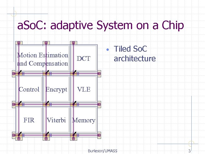
a. So. C: adaptive System on a Chip • Motion Estimation and Compensation DCT Control Encrypt Tiled So. C architecture VLE FIR Viterbi Memory Burleson/UMASS 3
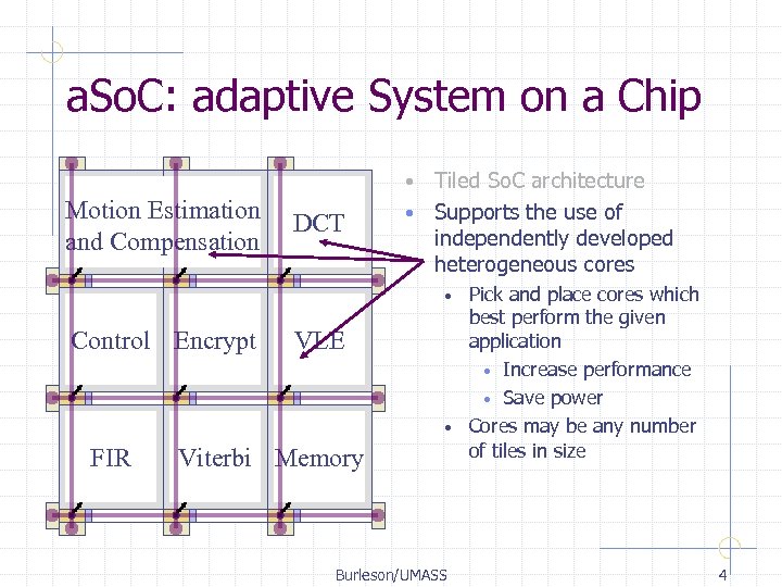
a. So. C: adaptive System on a Chip Tiled So. C architecture • Supports the use of independently developed heterogeneous cores • Motion Estimation and Compensation DCT Pick and place cores which best perform the given application • Increase performance • Save power • Cores may be any number of tiles in size • Control Encrypt FIR VLE Viterbi Memory Burleson/UMASS 4
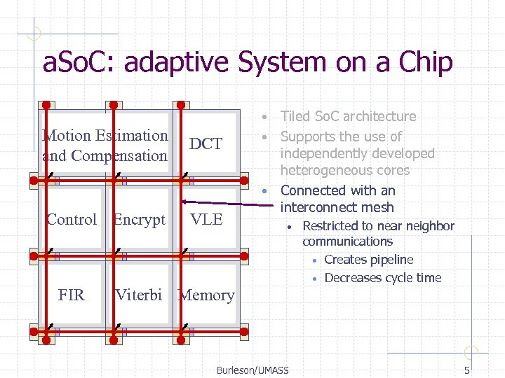
a. So. C: adaptive System on a Chip Tiled So. C architecture • Supports the use of independently developed heterogeneous cores • Connected with an interconnect mesh • Motion Estimation and Compensation DCT Control Encrypt VLE FIR • Restricted to near neighbor communications • Creates pipeline • Decreases cycle time Viterbi Memory Burleson/UMASS 5
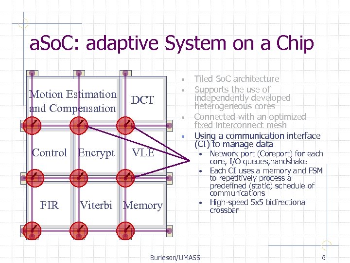
a. So. C: adaptive System on a Chip Motion Estimation and Compensation DCT • • Control Encrypt VLE Tiled So. C architecture Supports the use of independently developed heterogeneous cores Connected with an optimized fixed interconnect mesh Using a communication interface (CI) to manage data • • FIR Viterbi Memory • Burleson/UMASS Network port (Coreport) for each core, I/O queues, handshake Each CI uses a memory and FSM to repetitively process a predefined (static) schedule of communications High-speed 5 x 5 bidirectional crossbar 6
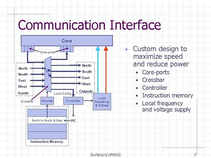
Communication Interface Core • Core-ports North Custom design to maximize speed and reduce power South East • East South • West Inputs Local Config. • Outputs Decoder Controller North to South & East Local Frequency & Voltage • Core-ports Crossbar Controller Instruction memory Local frequency and voltage supply PC Crossbar • Instruction Memory Burleson/UMASS 7
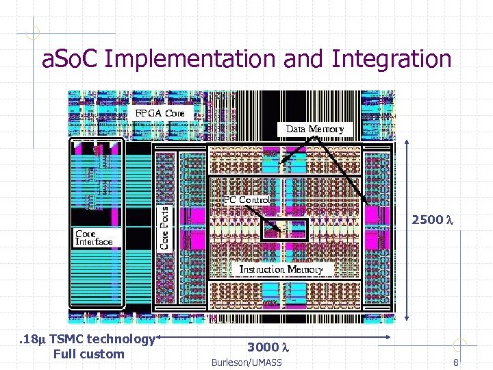
a. So. C Implementation and Integration 2500 l . 18 m TSMC technology Full custom 3000 l Burleson/UMASS 8
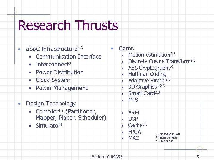
Research Thrusts • • a. So. C Infrastructure 1, 3 • Communication Interface • Interconnect 3 • Power Distribution • Clock System • Power Management Design Technology • Compiler 1, 3 (Partitioner, Mapper, Placer, Scheduler) • Simulator 1 • Cores • • Motion estimation 2, 3 Discrete Cosine Transform 2, 3 AES Cryptography 3 Huffman Coding Adaptive Viterbi 2, 3 3 D Graphics 1, 2, 3 Smart Card 2, 3 MP 3 • • • ARM DSP Cache 2, 3 FPGA MAC Burleson/UMASS 1 2 3 Ph. D Dissertation Masters Thesis Publications 9
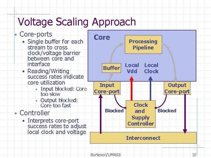
Voltage Scaling Approach • Core-ports Single buffer for each stream to cross clock/voltage barrier between core and interface • Reading/Writing success rates indicate core utilization • Input blocked: Core too slow • Output blocked: Core too fast • • Controller • Interprets core-port success rates to adjust local clock and voltage Core Buffer Processing Pipeline Local Vdd Clock Input Core-port Output Core-port Clock Blocked and Supply Controller Interconnect Burleson/UMASS 10
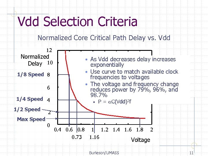
Vdd Selection Criteria Normalized Core Critical Path Delay vs. Vdd 12 Normalized Delay 10 1/8 Speed 8 6 1/4 Speed 4 1/2 Speed As Vdd decreases delay increases exponentially • Use curve to match available clock frequencies to voltages • The voltage and frequency change reduces power by 79%, 96%, and 98. 7% • • P = a. C(Vdd)2 f 2 Max Speed 0 0. 4 0. 6 0. 8 1 1. 2 1. 4 1. 6 1. 8 0. 73 1. 16 2 Voltage Burleson/UMASS 11
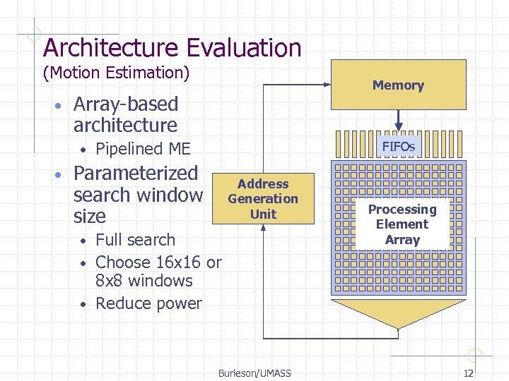
Architecture Evaluation (Motion Estimation) • Array-based architecture • • Memory Pipelined ME FIFOs Parameterized search window size Address Generation Unit Full search • Choose 16 x 16 or 8 x 8 windows • Reduce power • Burleson/UMASS Processing Element Array 12
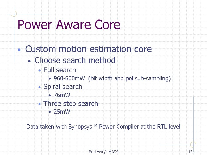
Power Aware Core • Custom motion estimation core • Choose search method • Full search • • Spiral search • • 960 -600 m. W (bit width and pel sub-sampling) 76 m. W Three step search • 25 m. W Data taken with Synopsys. TM Power Compiler at the RTL level Burleson/UMASS 13
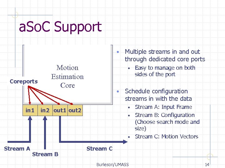
a. So. C Support • Coreports in 1 Stream A Motion Estimation Core • • Easy to manage on both sides of the port Schedule configuration streams in with the data Stream A: Input Frame • Stream B: Configuration (Choose search mode and size) • Stream C: Motion Vectors • in 2 out 1 out 2 Stream B Multiple streams in and out through dedicated core ports Stream C Burleson/UMASS 14
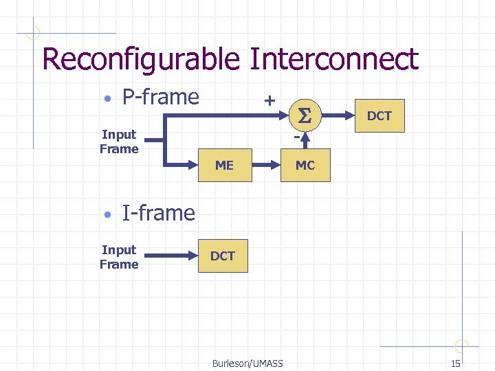
Reconfigurable Interconnect • P-frame + DCT - Input Frame ME • S MC I-frame Input Frame DCT Burleson/UMASS 15
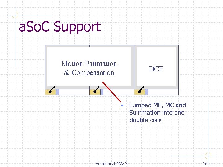
a. So. C Support Motion Estimation & Compensation DCT • Burleson/UMASS Lumped ME, MC and Summation into one double core 16
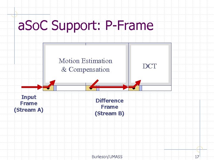
a. So. C Support: P-Frame Motion Estimation & Compensation Input Frame (Stream A) DCT Difference Frame (Stream B) Burleson/UMASS 17
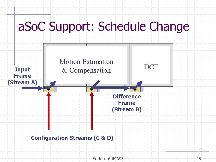
a. So. C Support: Schedule Change Input Frame (Stream A) Motion Estimation & Compensation DCT Difference Frame (Stream B) Configuration Streams (C & D) Burleson/UMASS 18
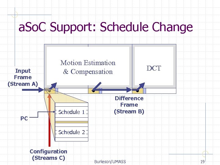
a. So. C Support: Schedule Change Input Frame (Stream A) PC Motion Estimation & Compensation Schedule 1 DCT Difference Frame (Stream B) Schedule 2 Configuration (Streams C) Burleson/UMASS 19
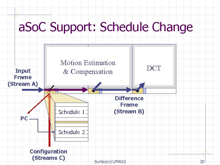
a. So. C Support: Schedule Change Input Frame (Stream A) PC Motion Estimation & Compensation Schedule 1 DCT Difference Frame (Stream B) Schedule 2 Configuration (Streams C) Burleson/UMASS 20
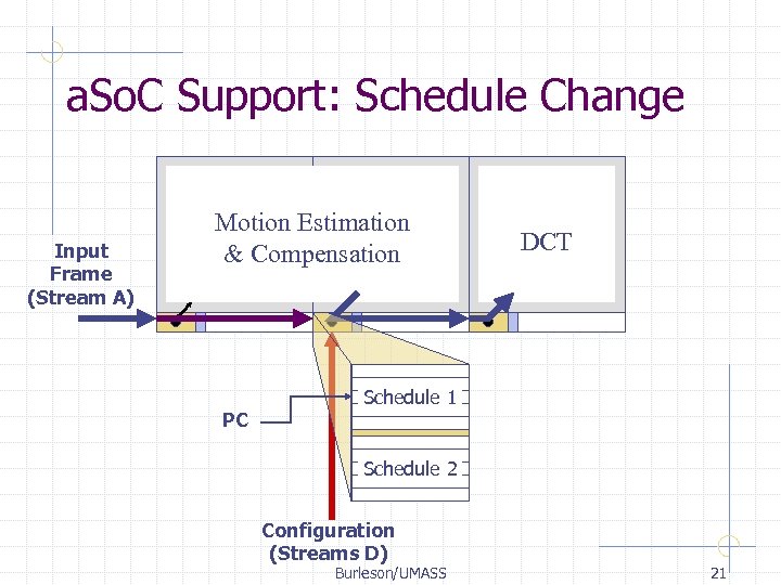
a. So. C Support: Schedule Change Input Frame (Stream A) Motion Estimation & Compensation PC DCT Schedule 1 Schedule 2 Configuration (Streams D) Burleson/UMASS 21
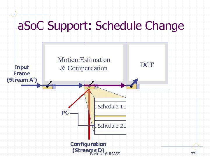
a. So. C Support: Schedule Change Input Frame (Stream A’) Motion Estimation & Compensation PC DCT Schedule 1 Schedule 2 Configuration (Streams D) Burleson/UMASS 22
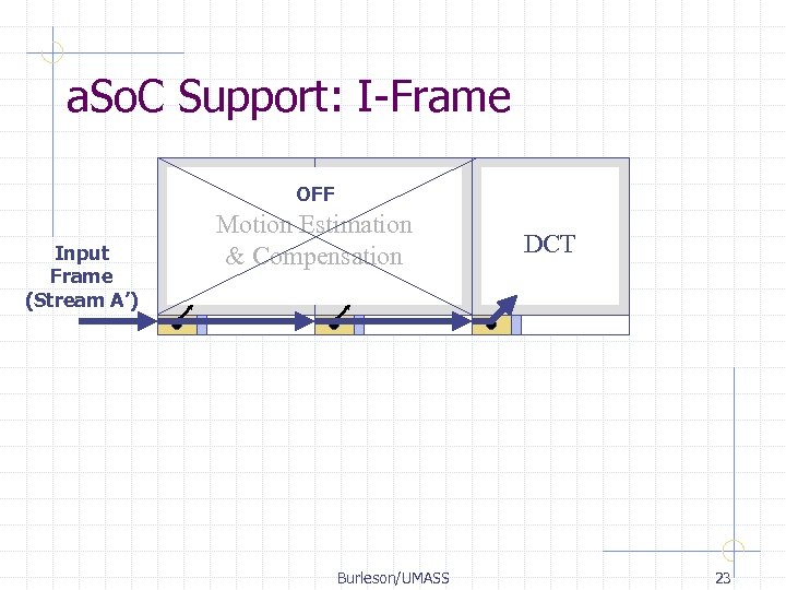
a. So. C Support: I-Frame OFF Input Frame (Stream A’) Motion Estimation & Compensation Burleson/UMASS DCT 23
Operating Frequency? • Interconnect synchronized • • H-tree clock distribution Core frequencies depend on critical path Tile provides clock reference • Coreport provides asynchronous boundary • • Dynamic core configuration requires dynamic clock configuration a. So. C clock reference provides multiples of interconnect clock (… 4 x, 2 x, 1 x, 0. 5 x, 0. 25 x, …) • Configured through the tile controller • Burleson/UMASS 24
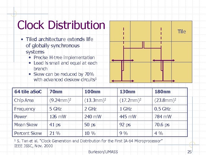
Clock Distribution Tile • Tiled architecture extends life of globally synchronous systems • Precise H-tree implementation • Load is small and equal at each branch • Skew can be reduced by 70% with advanced deskew circuits 1 64 tile a. So. C 70 nm 100 nm 130 nm 180 nm Chip Area (9. 24 mm)2 (13. 3 mm)2 (17. 2 mm)2 (23. 8 mm)2 Frequency 5 GHz 2 GHz 1 GHz 0. 5 GHz Power 126 m. W 240 m. W 445 m. W 784 m. W Mean Skew 41 ps 50 ps 92 ps 70. 6 ps Percent Skew 21 % 10 % 9% 4% S. Tan et al. “Clock Generation and Distribution for the First IA-64 Microprocessor” IEEE JSSC, Nov. 2000 Burleson/UMASS 1 25
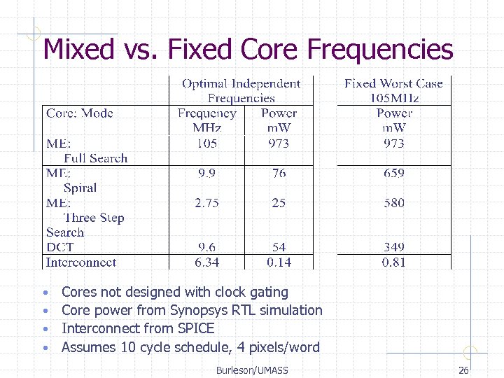
Mixed vs. Fixed Core Frequencies Cores not designed with clock gating • Core power from Synopsys RTL simulation • Interconnect from SPICE • Assumes 10 cycle schedule, 4 pixels/word • Burleson/UMASS 26
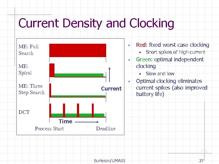
Current Density and Clocking • ME: Full Search Red: fixed worst case clocking • • ME: Spiral Green: optimal independent clocking • ME: Three Step Search • Current Short spikes of high current Slow and low Optimal clocking eliminates current spikes (also improved battery life) DCT Time Process Start Deadline Burleson/UMASS 27
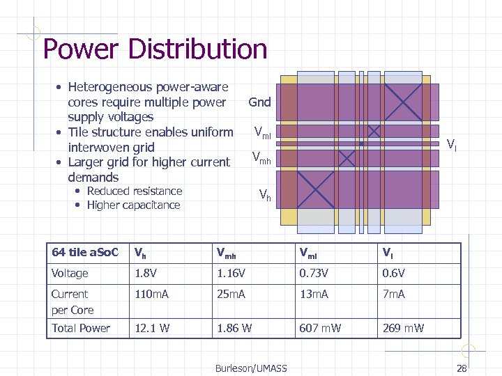
Power Distribution • Heterogeneous power-aware cores require multiple power supply voltages • Tile structure enables uniform interwoven grid • Larger grid for higher current demands Gnd Vml Vl Vmh • Reduced resistance • Higher capacitance Vh 64 tile a. So. C Vh Vml Vl Voltage 1. 8 V 1. 16 V 0. 73 V 0. 6 V Current per Core 110 m. A 25 m. A 13 m. A 7 m. A Total Power 12. 1 W 1. 86 W 607 m. W 269 m. W Burleson/UMASS 28
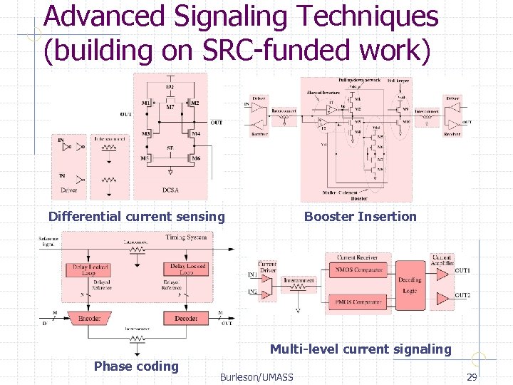
Advanced Signaling Techniques (building on SRC-funded work) Differential current sensing Booster Insertion Multi-level current signaling Phase coding Burleson/UMASS 29
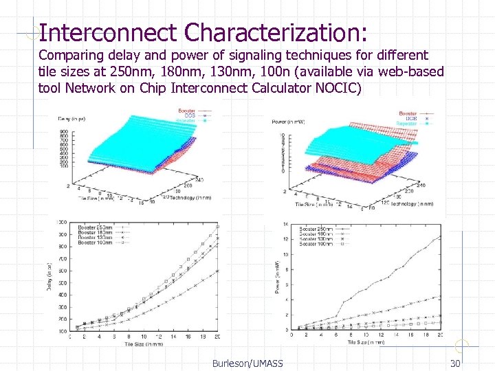
Interconnect Characterization: Comparing delay and power of signaling techniques for different tile sizes at 250 nm, 180 nm, 130 nm, 100 n (available via web-based tool Network on Chip Interconnect Calculator NOCIC) Burleson/UMASS 30
Conclusions • Regular Tiled Architecture • • Static scheduling • • • High-level global schedule of inter-core communication Accomodates dynamic workloads with queues and local handshakes Demonstration using Motion Estimation and DCT • • Task-based parallelism using heterogeneous cores Predictable interconnect Regular core interface, Vdd and clock control, and configuration control Variable search window and search algorithm provide power/quality tradeoff Power savings using scalable approaches to dynamic clock and power variation • • Simple clock dividers leveraging existing clock distribution methods Route multiple power supplies to allow rapid switching and avoid overhead of on-chip power regulation Burleson/UMASS 31
Ongoing Work • Satellite Set-top Box application • • New and more complete wireless and multimedia systems • • Jpeg 2000, mpeg-4, 3 d Graphics, … ASOC parameter optimization • • Developed at Hughes Networks using 7 distinct RISC cores. Compare ASOC with in-house shared memory approach for interconnections. Tile sizes, bus widths, clocks, VDDs Coping with Core irregularity • Size, I/O positions, shapes, bus widths, communication interfaces • • Interconnect circuit optimization (No. CIC) Leakage Power issues Reliability, Test, Fault-Tolerance and Security Compilation: especially Partitioning, Mapping • Prototypes: . 18 u MOSIS of communication interface, ~25 K transistors, verification of interface logic and timing ASOC in Education: Circuits, architecture and core design projects • Burleson/UMASS 32
Implications (perhaps controversial ) • • • Multi-core architectures will be needed to maintain Moore’s law (interconnect, memory, parallelism) Task-based parallelism may be easier to program, extract and implement than data parallelism (think multi-core rather than instruction level parallelism) Global coarse synchronization provides an approach to hard-real time computing for dynamic workloads (ie video coding). Dynamic Power savings exploiting fine-grain workload variations can be achieved through straightforward clock and power scaling methods. Interconnect standards will be specified by silicon foundries similar to cell libraries and memories Burleson/UMASS 33
Design Flow http: //vsp 2. ecs. umass. edu/vspg/658/TA_Tools/design_flow. html • Architecture to Layout • • • Architecture: Block diagram of system and behavioral description Logic: Gate level or schematic description Circuit: Transistor configurations and sizings Layout: Floorplanning, clock and power distribution Tools • • Verilog. XL: behavioral representation VTVT: standard cell library Synopsys: standard cell gate level netlist generation Silicon Ensemble: standard cell netlist to layout Cadence Layout. Plus: schematic and layout design NCSU CDK: design and extraction rules Cadence Layout vs. Schematic: layout verification HSPICE: circuit simulator Burleson/UMASS 34
9016cefc75c56bc1fd553819d66094ee.ppt