c631af874a8e01e23b81870c416ca29c.ppt
- Количество слайдов: 35
 Adaptive On-Chip Test Strategies for Complex Systems V. Stopjaková Department of Microelectronics, STU Bratislava, Slovakia 1
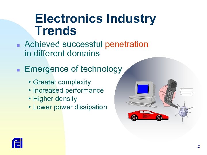 Electronics Industry Trends n n Achieved successful penetration in different domains Emergence of technology • Greater complexity • Increased performance • Higher density • Lower power dissipation 2
 Market-Driven Products n Meet user Quality requirements u n Created an unprecedented Dependency u n satisfying users to buy products market-driven products Maintain competitive by providing: Greater Product Functionality u Lower Cost u Reduced Interval (time to market) u Higher Reliability u 3
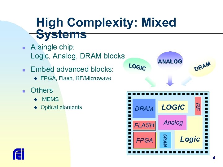 High Complexity: Mixed Systems n n A single chip: Logic, Analog, DRAM blocks Embed advanced blocks: u n LOGI C ANALOG M RA D FPGA, Flash, RF/Microwave Others u DRAM LOGIC FLASH RF u MEMS Optical elements Analog SRAM FPGA Logic 4
 High Complexity: Mixed Systems n n n How to test the mixed chip? With external test only - need multiple ATE for a single chip: Logic ATE, Memory ATE, Analog ATE (Double/Triple Insertion) Need special ATE with combined capabilities 5
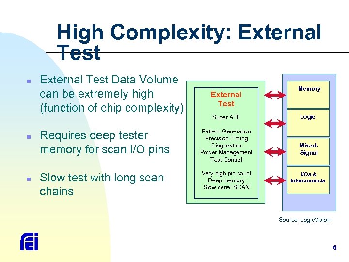 High Complexity: External Test n External Test Data Volume can be extremely high (function of chip complexity) External Test Super ATE n n Requires deep tester memory for scan I/O pins Pattern Generation Precision Timing Diagnostics Power Management Test Control Slow test with long scan chains Very high pin count Deep memory Slow serial SCAN Memory Logic Mixed. Signal I/Os & Interconnects Source: Logic. Vision 6
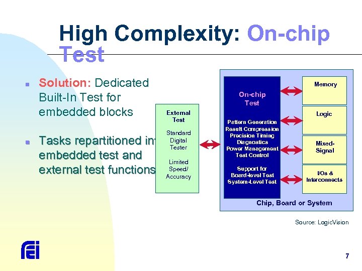 High Complexity: On-chip Test n n Solution: Dedicated Built-In Test for embedded blocks Memory On-chip Test External Test Standard Digital Tester Tasks repartitioned into embedded test and Limited Speed/ external test functions Accuracy Logic Pattern Generation Result Compression Precision Timing Diagnostics Power Management Test Control Support for Board-level Test System-Level Test Mixed. Signal I/Os & Interconnects Chip, Board or System Source: Logic. Vision 7
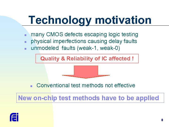 Technology motivation n many CMOS defects escaping logic testing physical imperfections causing delay faults unmodeled faults (weak-1, weak-0) Quality & Reliability of IC affected ! n Conventional test methods not effective New on-chip test methods have to be applied 8
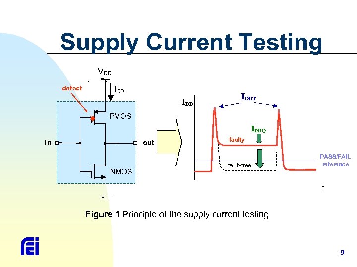 Supply Current Testing VDD defect I DD IDDT PMOS IDDQ in out NMOS faulty fault-free PASS/FAIL reference t Figure 1 Principle of the supply current testing 9
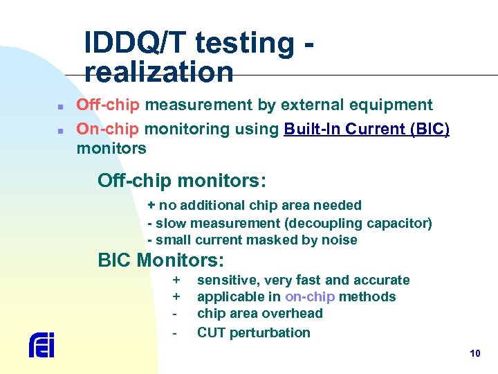 IDDQ/T testing realization n n Off-chip measurement by external equipment On-chip monitoring using Built-In Current (BIC) monitors Off-chip monitors: + no additional chip area needed - slow measurement (decoupling capacitor) - small current masked by noise BIC Monitors: + + - sensitive, very fast and accurate applicable in on-chip methods chip area overhead CUT perturbation 10
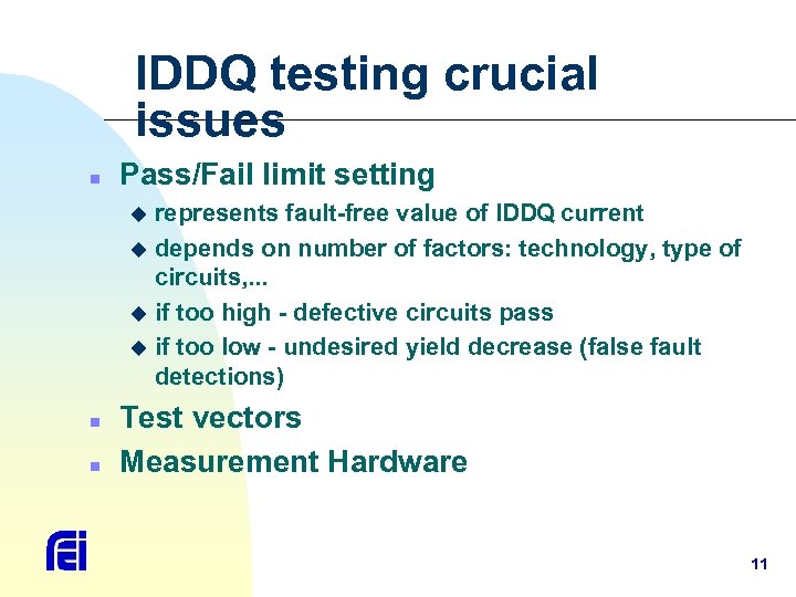 IDDQ testing crucial issues n Pass/Fail limit setting represents fault-free value of IDDQ current u depends on number of factors: technology, type of circuits, . . . u if too high - defective circuits pass u if too low - undesired yield decrease (false fault detections) u n n Test vectors Measurement Hardware 11
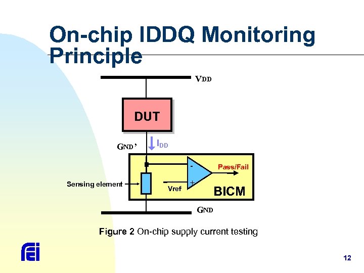 On-chip IDDQ Monitoring Principle VDD DUT GND’ IDD - Sensing element Vref + Pass/Fail BICM GND Figure 2 On-chip supply current testing 12
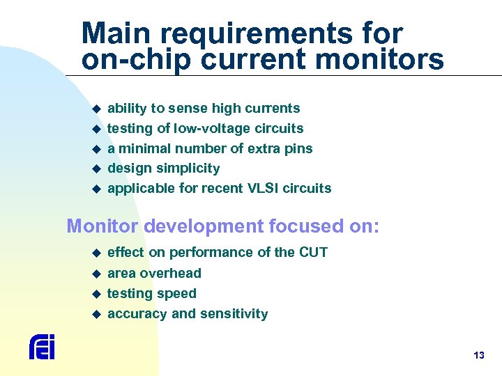 Main requirements for on-chip current monitors u u u ability to sense high currents testing of low-voltage circuits a minimal number of extra pins design simplicity applicable for recent VLSI circuits Monitor development focused on: u u effect on performance of the CUT area overhead testing speed accuracy and sensitivity 13
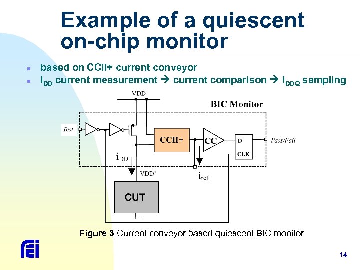 Example of a quiescent on-chip monitor n n based on CCII+ current conveyor IDD current measurement current comparison IDDQ sampling Figure 3 Current conveyor based quiescent BIC monitor 14
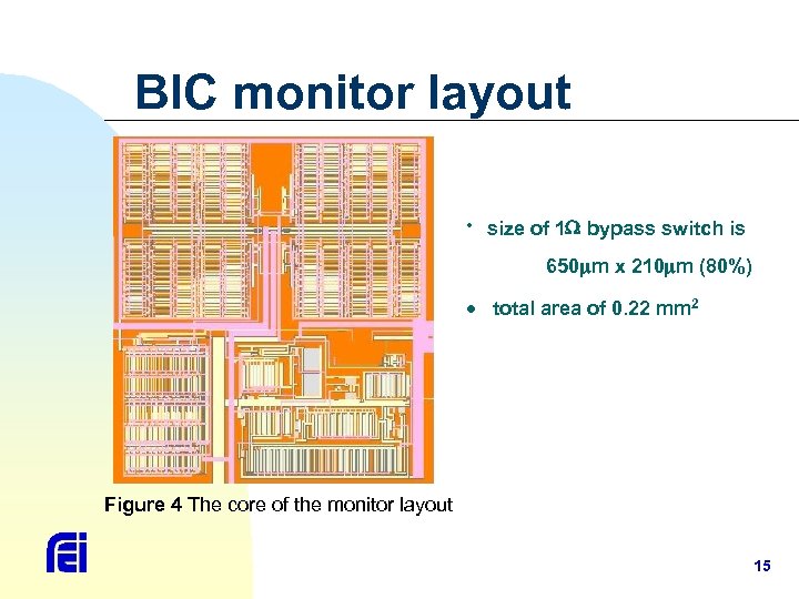 BIC monitor layout · size of 1 bypass switch is 650 m x 210 m (80%) · total area of 0. 22 mm 2 Figure 4 The core of the monitor layout 15
 Evaluation results n n n resolution of 10 n. A Pass/Fail limit of 50 n. A (sensitivity) 1 MHz testing speed VDD degradation max. 100 m. V area overhead of 0. 22 mm 2 ability to handle large CMOS IC 16
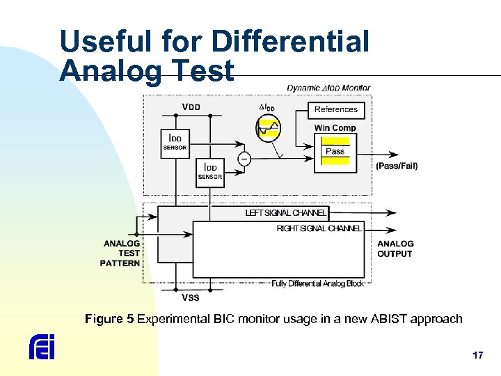 Useful for Differential Analog Test Figure 5 Experimental BIC monitor usage in a new ABIST approach 17
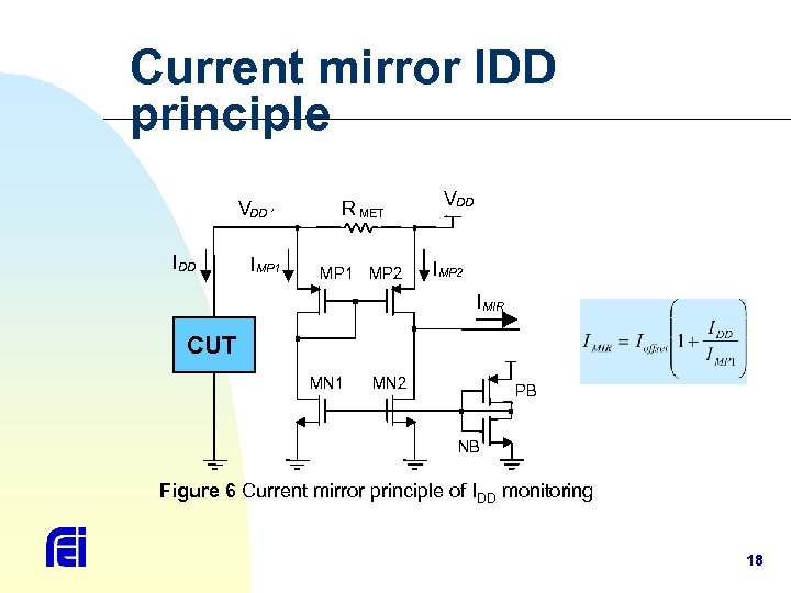 Current mirror IDD principle VDD ’ I DD I MP 1 R MET MP 1 MP 2 VDD I MP 2 I MIR CUT MN 1 MN 2 PB NB Figure 6 Current mirror principle of IDD monitoring 18
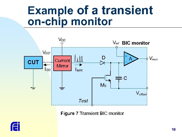 Example of a transient on-chip monitor VDD Vref BIC monitor VDD’ CUT I DD Current Mirror D Vmon A I MIR C MS Voffset Test Figure 7 Transient BIC monitor 19
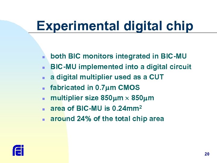 Experimental digital chip n n n n both BIC monitors integrated in BIC-MU implemented into a digital circuit a digital multiplier used as a CUT fabricated in 0. 7 m CMOS multiplier size 850 m area of BIC-MU is 0. 24 mm 2 around 24% of the total chip area 20
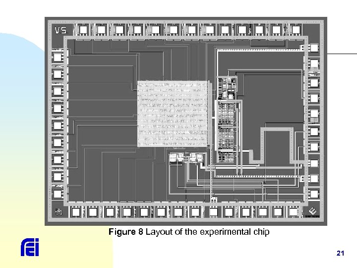 Figure 8 Layout of the experimental chip 21
 Versatility Problem of IDD Testing n n IDD testing proven very successful for digital circuits Dedicated fault class only Use in submicron technologies limited IDD testing for analog IC not straightforward Large variety of analog IC F Specifications and behavior unique F Difficult to generalize analog tests F Validation up to now done using functional criteria F Current consumption analysis using Neural Networks 22
 Artificial Neural Networks Approach n n n Current signature analysis for presence of abnormal (faulty) behavior Massively parallel and distributed structures capable of adaptation No explicit Pass/Fail limit formulation required Excellent versatility Accuracy and sensitivity Reduced number of TP (time to test) 23
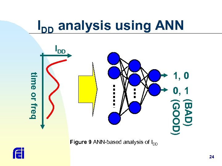 IDD analysis using ANN IDD time or freq 1, 0 0, 1 (BAD) (GOOD) Figure 9 ANN-based analysis of IDD 24
 Mathematical model x 1 wk 1 x. P w k. P bk uk (uk) yk Figure 10 Mathematical model of an artificial neuron 25
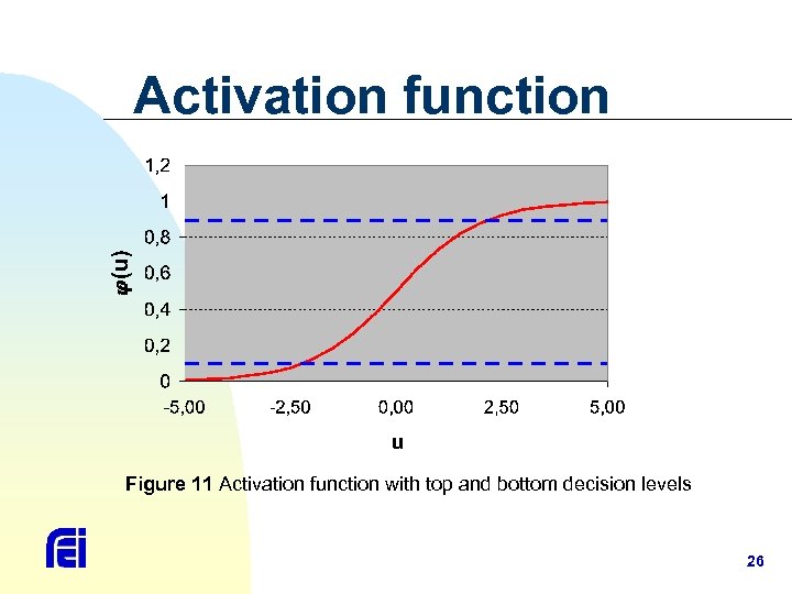 Activation function Figure 11 Activation function with top and bottom decision levels 26
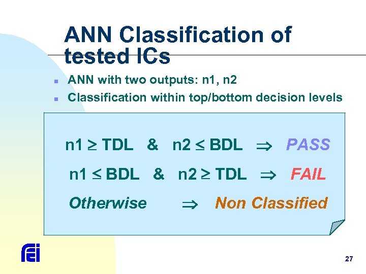 ANN Classification of tested ICs n n ANN with two outputs: n 1, n 2 Classification within top/bottom decision levels n 1 TDL & n 2 BDL PASS n 1 BDL & n 2 TDL FAIL Otherwise Non Classified 27
 Analog DUT Example n Two-stage CMOS operational amplifier n A pulse used as input stimuli n n Good patterns: technology parameters and temperature variations Faulty behavior: basic defects injected (GOS, DOP, SOP, DSS, GDS) 28
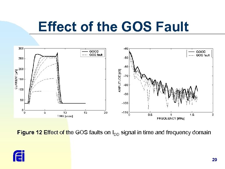 Effect of the GOS Fault Figure 12 Effect of the GOS faults on IDD signal in time and frequency domain 29
 Effect of the DSS Fault Figure 13 Effect of the DSS fault on IDD signal in different domains 30
 ANN setup n n n n n 660 tested power supply current waveforms 200 faulty patterns 460 fault-free patterns 32 input nodes various training set: 200, 100, 76, 50 and 26 various number of hidden units: 2, 6, 10, 14, 18, 22 top decision level: 0. 9 bottom decision level: 0. 1 10 independent measurements 31
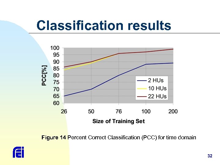 Classification results Figure 14 Percent Correct Classification (PCC) for time domain 32
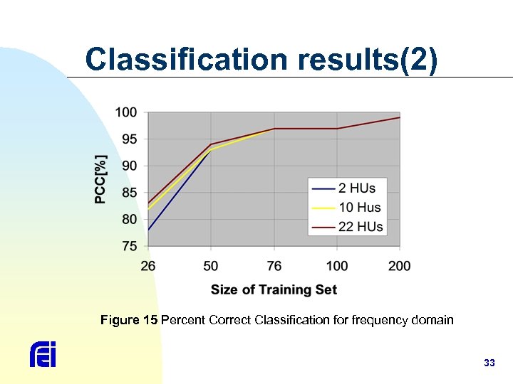 Classification results(2) Figure 15 Percent Correct Classification for frequency domain 33
 Conclusions n To ensure quality of So. C Technologies: u n n n On-chip Test is added into the designs of embedded cores New adaptive on-chip approaches needed for different test functions On-chip current monitoring effective but not versatile and limited to CMOS digital circuit ANN classification of defective IC u u u ability of testing mixed-signal circuits ability of sensing negligible differences possibility to analyse other circuit’s parameters 34
 Thank YOU for your attention! 35


