203456222a0e07d1e6e0eb66ae53a766.ppt
- Количество слайдов: 11
 ACTFEL Alternating Current Thin Film Electroluminescent Lamps
 Objective Ü Use photolithography to pattern ITO Ü Develop photoresist and etch ITO Ü Apply layers of phosphors, dielectric, and silver Ü Power up lamp Ü Troubleshoot
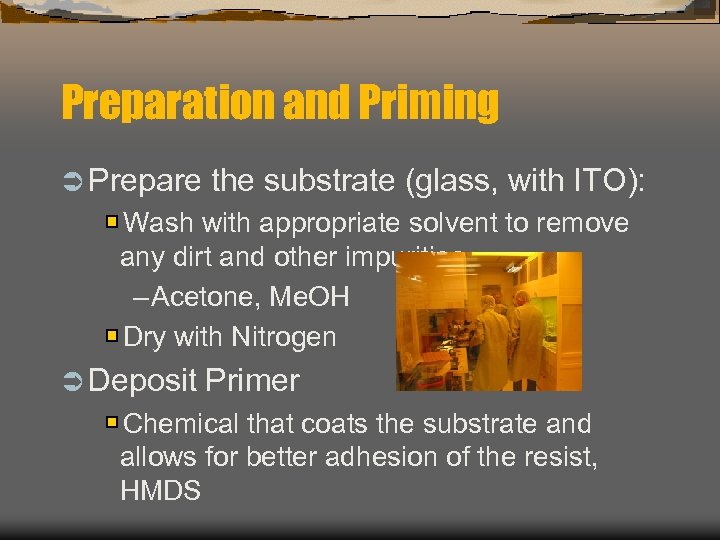 Preparation and Priming Ü Prepare the substrate (glass, with ITO): Wash with appropriate solvent to remove any dirt and other impurities – Acetone, Me. OH Dry with Nitrogen Ü Deposit Primer Chemical that coats the substrate and allows for better adhesion of the resist, HMDS
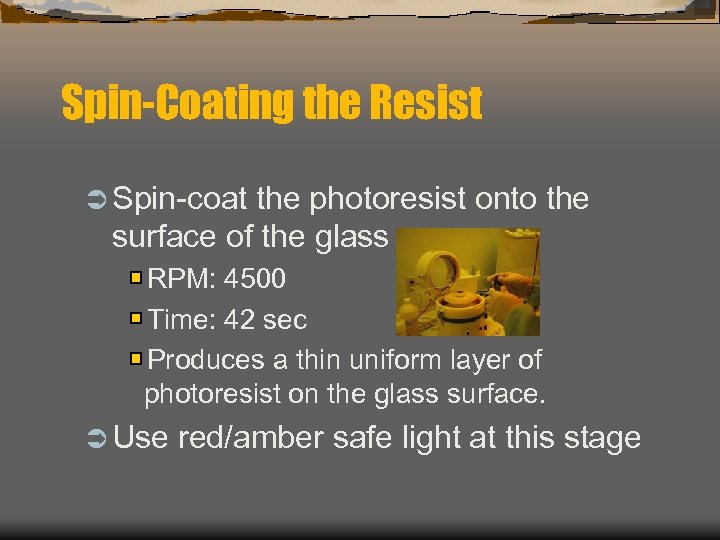 Spin-Coating the Resist Ü Spin-coat the photoresist onto the surface of the glass RPM: 4500 Time: 42 sec Produces a thin uniform layer of photoresist on the glass surface. Ü Use red/amber safe light at this stage
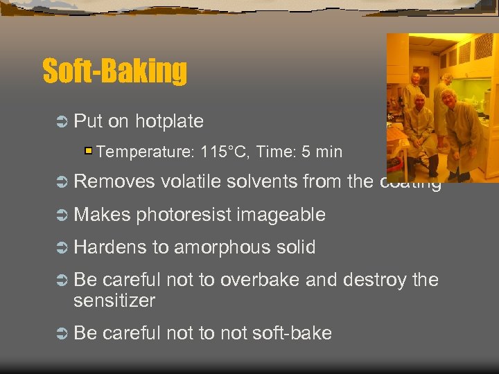 Soft-Baking Ü Put on hotplate Temperature: 115°C, Time: 5 min Ü Removes Ü Makes volatile solvents from the coating photoresist imageable Ü Hardens to amorphous solid Ü Be careful not to overbake and destroy the sensitizer Ü Be careful not to not soft-bake
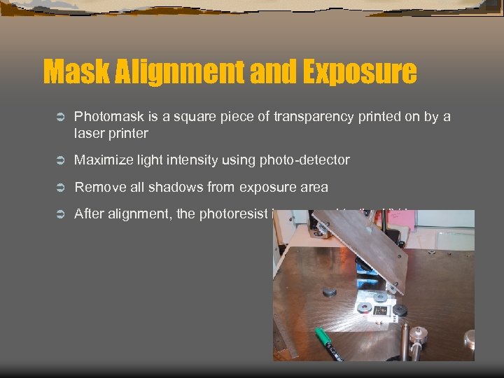 Mask Alignment and Exposure Ü Photomask is a square piece of transparency printed on by a laser printer Ü Maximize light intensity using photo-detector Ü Remove all shadows from exposure area Ü After alignment, the photoresist is exposed to the UV lamp
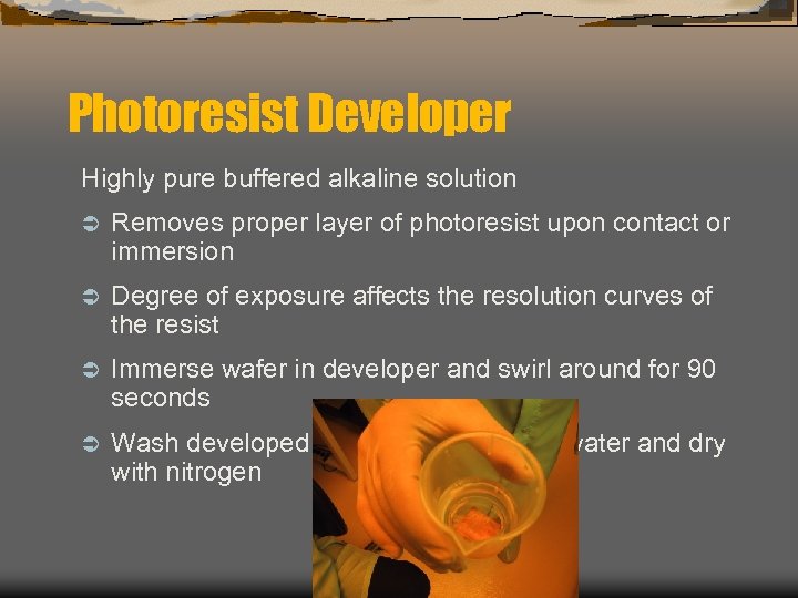 Photoresist Developer Highly pure buffered alkaline solution Ü Removes proper layer of photoresist upon contact or immersion Ü Degree of exposure affects the resolution curves of the resist Ü Immerse wafer in developer and swirl around for 90 seconds Ü Wash developed wafer with deionized water and dry with nitrogen
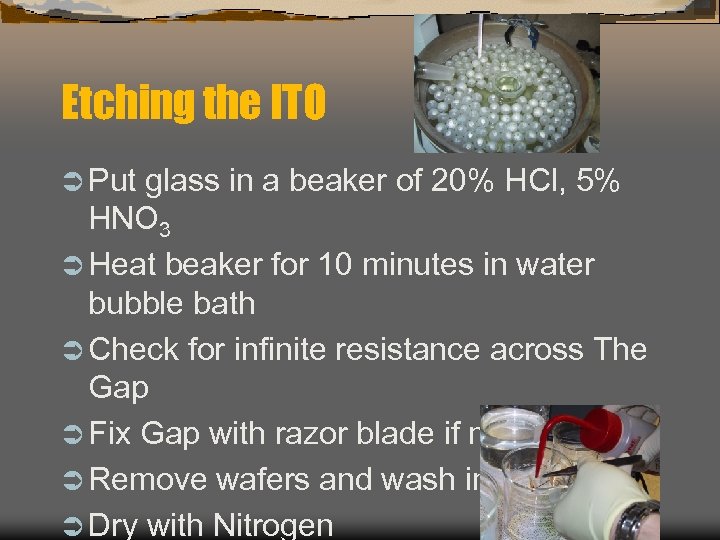 Etching the ITO Ü Put glass in a beaker of 20% HCl, 5% HNO 3 Ü Heat beaker for 10 minutes in water bubble bath Ü Check for infinite resistance across The Gap Ü Fix Gap with razor blade if necessary Ü Remove wafers and wash in acetone Ü Dry with Nitrogen
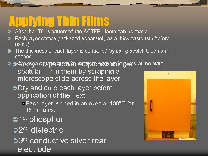 Applying Thin Films After the ITO is patterned the ACTFEL lamp can be made. Ü Each layer comes packaged separately as a thick paste (stir before using). Ü The thickness of each layer is controlled by using scotch tape as a spacer. Ü Ü Apply thetape along in sequence using a of the plate. Apply scotch pastes 3 -5 mm on two parallel sides Ü spatula. Thin them by scraping a microscope slide across the layer. Ü Dry and cure each layer before application of the next Each layer is dried in an oven at 130°C for 15 minutes. Ü 1 st phosphor Ü 2 nd dielectric Ü 3 rd conductive silver rear electrode
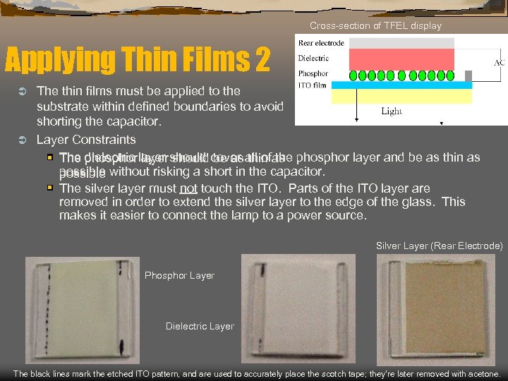 Cross-section of TFEL display Applying Thin Films 2 The thin films must be applied to the substrate within defined boundaries to avoid shorting the capacitor. Ü Layer Constraints dielectric layer should be as thin the The phosphor layer should cover all ofas phosphor layer and be as thin as possible without risking a short in the capacitor. The silver layer must not touch the ITO. Parts of the ITO layer are removed in order to extend the silver layer to the edge of the glass. This makes it easier to connect the lamp to a power source. Ü Silver Layer (Rear Electrode) Phosphor Layer Dielectric Layer The black lines mark the etched ITO pattern, and are used to accurately place the scotch tape; they’re later removed with acetone.
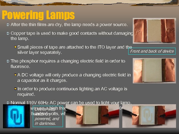 Powering Lamps Ü After the thin films are dry, the lamp needs a power source. Ü Copper tape is used to make good contacts without damaging the lamp. Small pieces of tape are attached to the ITO layer and the Front and back of device silver layer separately. Ü The phosphor requires a changing electric field in order to fluoresce. A DC voltage will only produce a changing electric field in a capacitor as it charges. In order to produce continuous lighting an AC voltage is required. Ü Normal 110 V 60 Hz AC power can be used to light your lamp. In the lab we use awith frequency power supply 60 -2000 Hz Device high and a few hundred volts, which gives a brighter light. leads on, powered, and in darkness.


