3a4a2e9deddb581b87dd6358576f5186.ppt
- Количество слайдов: 13
A Possible Solution to Fit in the MSU Requirements N. Usher (MSU/NSCL) ACTAR Workshop, June 17, 2008
A-A Physical Requirements n A-A must be less than 1. 4 cm thick (including shielding/cooling plates) n n n Width constraint is at inside of outer ring If inner edge of board is tapered, the rest of the board can exceed 1. 4 cm thick Alternative is to decrease board width (may not be possible)
Co. Bo Requirements Radial design prevents Co. Bo from being mounted astride A-A boards as in T 2 K design n Co. Bo will be installed outside the detector n n n Single-wide NIM module Transmit high-speed data using LVDS n Use two LVDS pairs per channel to decrease data rate requirements
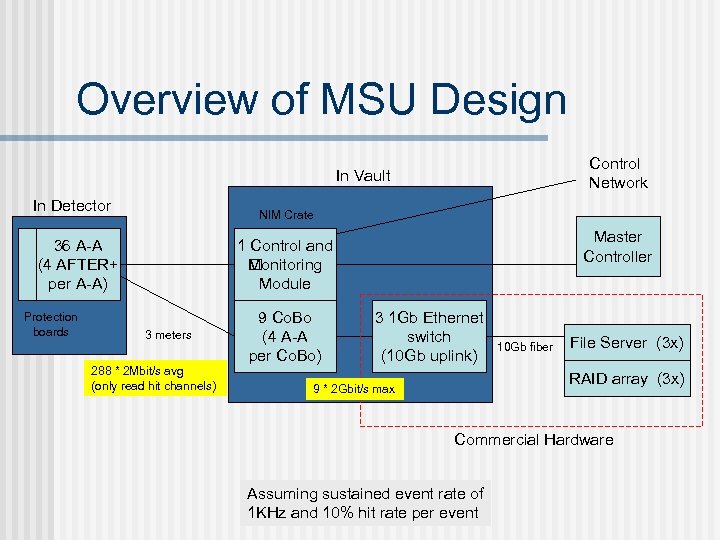
Overview of MSU Design Control Network In Vault In Detector NIM Crate 36 A-A (4 AFTER+ per A-A) Protection boards Master Controller 1 Control and M onitoring Module 3 meters 288 * 2 Mbit/s avg (only read hit channels) 9 Co. Bo (4 A-A per Co. Bo) 3 1 Gb Ethernet switch (10 Gb uplink) 10 Gb fiber File Server (3 x) RAID array (3 x) 9 * 2 Gbit/s max Commercial Hardware Assuming sustained event rate of 1 KHz and 10% hit rate per event
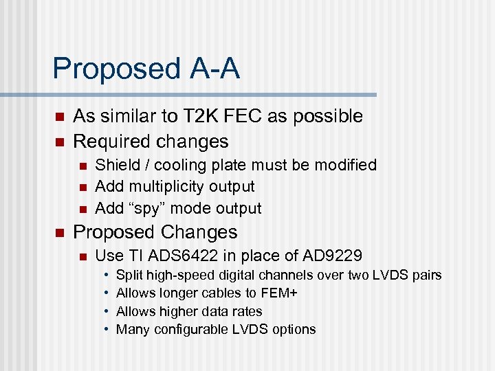
Proposed A-A n n As similar to T 2 K FEC as possible Required changes n n Shield / cooling plate must be modified Add multiplicity output Add “spy” mode output Proposed Changes n Use TI ADS 6422 in place of AD 9229 • • Split high-speed digital channels over two LVDS pairs Allows longer cables to FEM+ Allows higher data rates Many configurable LVDS options
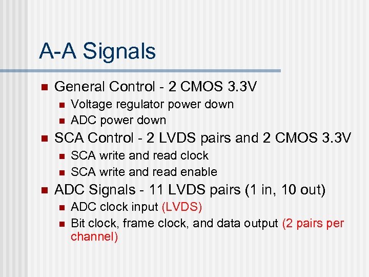
A-A Signals n General Control - 2 CMOS 3. 3 V n n n SCA Control - 2 LVDS pairs and 2 CMOS 3. 3 V n n n Voltage regulator power down ADC power down SCA write and read clock SCA write and read enable ADC Signals - 11 LVDS pairs (1 in, 10 out) n n ADC clock input (LVDS) Bit clock, frame clock, and data output (2 pairs per channel)
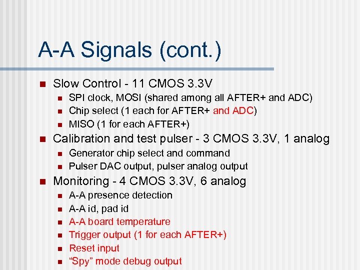
A-A Signals (cont. ) n Slow Control - 11 CMOS 3. 3 V n n Calibration and test pulser - 3 CMOS 3. 3 V, 1 analog n n n SPI clock, MOSI (shared among all AFTER+ and ADC) Chip select (1 each for AFTER+ and ADC) MISO (1 for each AFTER+) Generator chip select and command Pulser DAC output, pulser analog output Monitoring - 4 CMOS 3. 3 V, 6 analog n n n A-A presence detection A-A id, pad id A-A board temperature Trigger output (1 for each AFTER+) Reset input “Spy” mode debug output
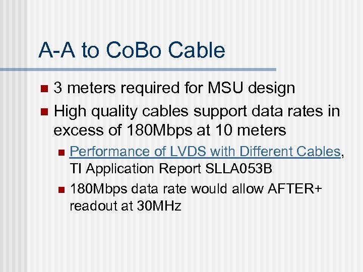
A-A to Co. Bo Cable 3 meters required for MSU design n High quality cables support data rates in excess of 180 Mbps at 10 meters n Performance of LVDS with Different Cables, TI Application Report SLLA 053 B n 180 Mbps data rate would allow AFTER+ readout at 30 MHz n
Proposed Co. Bo n Commercial FPGA starter board can be used for prototype n n n Virtex-4 or Virtex-5 Firmware development can begin as soon as specifications are finalized Production Cobo will be a single-width NIM module Zero suppression is critical - it will reduce data volume by at least 10 times Include peak fitting algorithm to further reduce data amount to be stored
Control / Monitoring Module Distribute timestamp, clock, and slow control to Co. Bos n Receive multiplicity signals from A-As n n Generate trigger signal Monitor A-A board temperatures n Handle AFTER+ “spy” mode signals n n Multiplex “spy” mode signals to allow display on oscilloscope
Master Controller Synchronizes multiple detectors n Generates timestamp clock n Receives trigger signal from each detector n n Sends external trigger to all detectors
Data Storage n n Active Target and Heavy Ion experiments represent two separate domains wrt data rates and volume Need flexible system that accommodates both n Active Target: • • n Channel occupancy < 1% Beam intensity will provide limiting factor to trigger rate (≥ 100 pps) Data rate < 2 MB/s Data volume ~ 350 GB (2 day expt) Heavy Ion: • • Channel occupancy < 10% Electronics will provide limiting factor to trigger rate Data rate < 250 MB/s Data volume dependent upon whether or not peak fitting is implemented in FPGA (provides x 100 reduction in volume) • Motivation => reduce data volume such that level 2 triggering based on tracking can be run online • Data Volume ~ 110 TB (5 day expt & assuming only zero suppression) • Clearly need additional data reduction beyond zero suppression!!!!
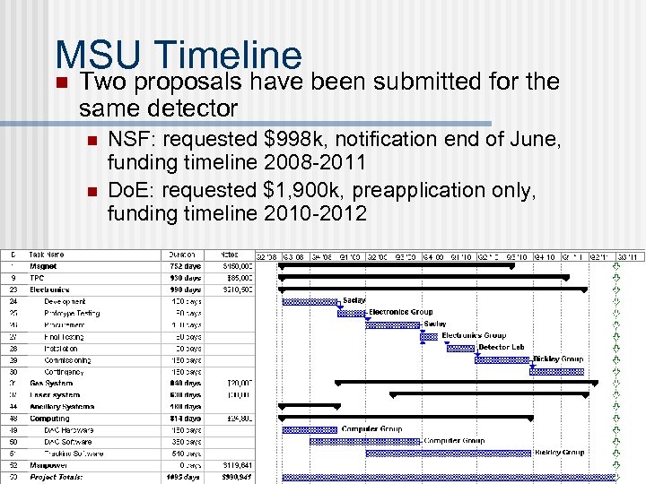
MSU Timeline n Two proposals have been submitted for the same detector n n NSF: requested $998 k, notification end of June, funding timeline 2008 -2011 Do. E: requested $1, 900 k, preapplication only, funding timeline 2010 -2012
3a4a2e9deddb581b87dd6358576f5186.ppt