913a27a20dde1e8cc8ae8deec95d8fa6.ppt
- Количество слайдов: 22
 9 th International Conference on Large Scale Applications and Radiation Hardness of Semiconductor Detectors, Florence, Italy RD 50 Collaboration – recent results on developing very high radiation resistant silicon detectors Otilia Militaru Université catholique de Louvain, Belgium on behalf of RD 50 http: //www. cern. ch/rd 50 01/10/2009 Otilia Militaru, on behalf of RD 50, RD 09 Conference, Italy
 RD 50 SUMMARY -Radiation environment and requirements for silicon sensors at Super LHC ; -Presentation of RD 50 Collaboration, members; -Some examples of the activities from several research directions within RD 50 Collaboration (this presentation explain only some recent results and does not cover all domains) ; Complete description one can find on the next RD 50 Status Report ; -Possible solutions for Super LHC silicon sensors ; http: //www. cern. ch/rd 50 01/10/2009 Otilia Militaru, on behalf of RD 50, RD 09 Conference, Italy 2
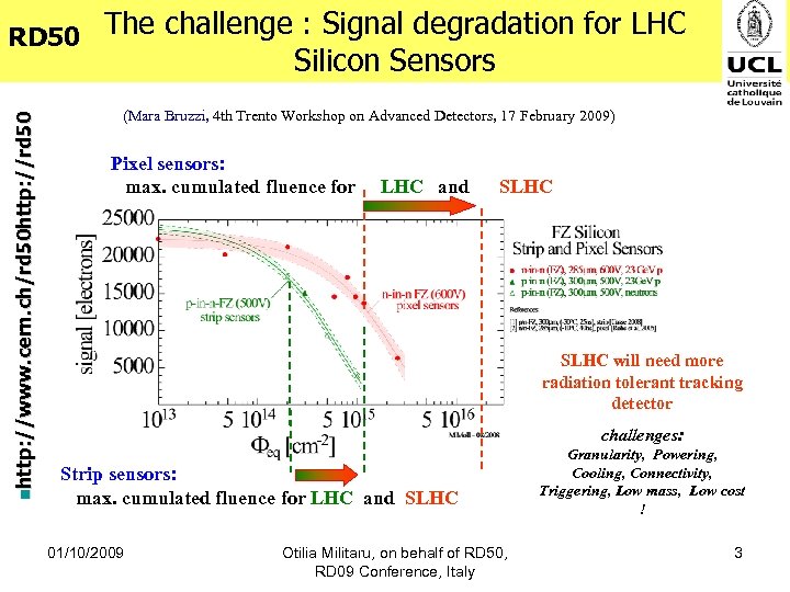 RD 50 The challenge : Signal degradation for LHC nhttp: //www. cern. ch/rd 50 http: //rd 50 Silicon Sensors (Mara Bruzzi, 4 th Trento Workshop on Advanced Detectors, 17 February 2009) Pixel sensors: max. cumulated fluence for LHC and SLHC will need more radiation tolerant tracking detector challenges: Strip sensors: max. cumulated fluence for LHC and SLHC 01/10/2009 Otilia Militaru, on behalf of RD 50, RD 09 Conference, Italy Granularity, Powering, Cooling, Connectivity, Triggering, Low mass, Low cost ! 3
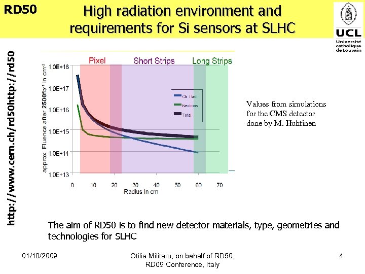 High radiation environment and requirements for Si sensors at SLHC http: //www. cern. ch/rd 50 http: //rd 50 RD 50 Values from simulations for the CMS detector done by M. Huhtinen The aim of RD 50 is to find new detector materials, type, geometries and technologies for SLHC 01/10/2009 Otilia Militaru, on behalf of RD 50, RD 09 Conference, Italy 4
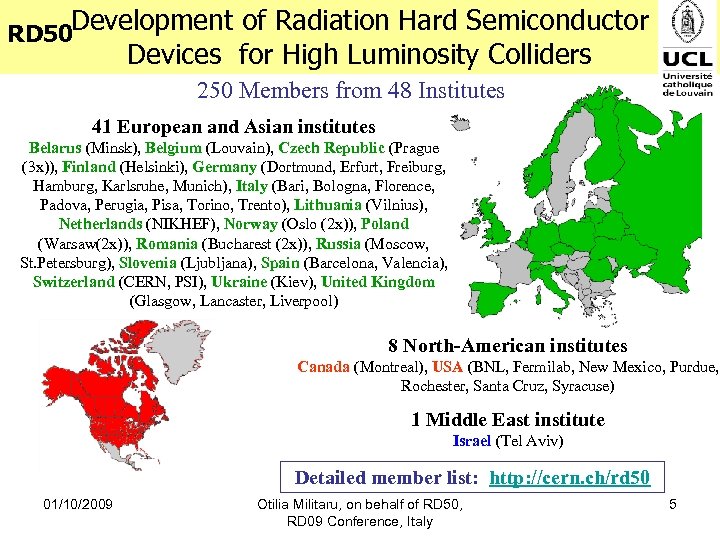 Development of Radiation Hard Semiconductor Devices for High Luminosity Colliders RD 50 250 Members from 48 Institutes 41 European and Asian institutes Belarus (Minsk), Belgium (Louvain), Czech Republic (Prague (3 x)), Finland (Helsinki), Germany (Dortmund, Erfurt, Freiburg, Hamburg, Karlsruhe, Munich), Italy (Bari, Bologna, Florence, Padova, Perugia, Pisa, Torino, Trento), Lithuania (Vilnius), Netherlands (NIKHEF), Norway (Oslo (2 x)), Poland (Warsaw(2 x)), Romania (Bucharest (2 x)), Russia (Moscow, St. Petersburg), Slovenia (Ljubljana), Spain (Barcelona, Valencia), Switzerland (CERN, PSI), Ukraine (Kiev), United Kingdom (Glasgow, Lancaster, Liverpool) 8 North-American institutes Canada (Montreal), USA (BNL, Fermilab, New Mexico, Purdue, Rochester, Santa Cruz, Syracuse) 1 Middle East institute Israel (Tel Aviv) Detailed member list: http: //cern. ch/rd 50 01/10/2009 Otilia Militaru, on behalf of RD 50, RD 09 Conference, Italy 5
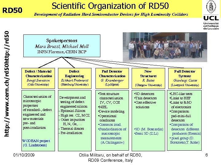 http: //www. cern. ch/rd 50 http: //rd 50 RD 50 Scientific Organization of RD 50 Development of Radiation Hard Semiconductor Devices for High Luminosity Colliders Spokespersons Mara Bruzzi, Michael Moll INFN Florence, CERN ECP Defect / Material Characterization Bengt Svensson Defect Engineering Eckhart Fretwurst Pad Detector Characterization G. Kramberger New Structures R. Bates Full Detector Systems Gianluigi Casse (Oslo University) (Hamburg University) (Ljubljana) (Glasgow University) (Liverpool University) Characterization of microscopic properties of standard-, defect engineered and new materials pre- and post-irradiation WODEAN project (G. Lindstroem) 01/10/2009 Development and testing of defect engineered silicon: - Epitaxial Silicon - High res. CZ, MCZ - Other impurities H, N, Ge, … - Thermal donors - Pre-irradiation • Test structure characterization IV, CCE • NIEL • Device modeling • Operational conditions • Common irrad. • Standardisation of macroscopic measurements (A. Chilingarov) • 3 D detectors • Thin detectors • Cost effective solutions • 3 D (M. Boscardin) • Semi 3 D (Z. Li) Otilia Militaru, on behalf of RD 50, RD 09 Conference, Italy • LHC-like tests • Links to HEP • Links to R&D of electronics • Comparison: pad-mini-full detectors • Comparison of detectors different producers (Eremin) • pixel group (D. Bortoletto, T. Rohe) 6
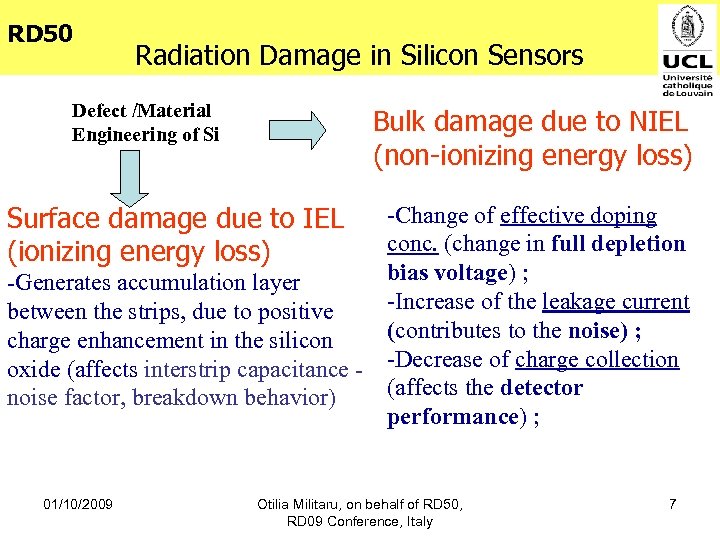 RD 50 Radiation Damage in Silicon Sensors Defect /Material Engineering of Si Bulk damage due to NIEL (non-ionizing energy loss) Surface damage due to IEL (ionizing energy loss) -Change of effective doping conc. (change in full depletion bias voltage) ; -Generates accumulation layer -Increase of the leakage current between the strips, due to positive (contributes to the noise) ; charge enhancement in the silicon oxide (affects interstrip capacitance - -Decrease of charge collection (affects the detector noise factor, breakdown behavior) performance) ; 01/10/2009 Otilia Militaru, on behalf of RD 50, RD 09 Conference, Italy 7
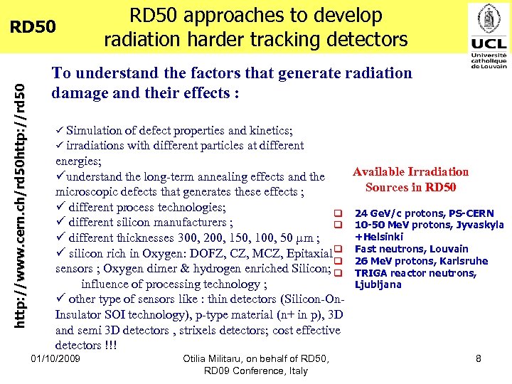 http: //www. cern. ch/rd 50 http: //rd 50 RD 50 approaches to develop radiation harder tracking detectors To understand the factors that generate radiation damage and their effects : ü Simulation of defect properties and kinetics; ü irradiations with different particles at different energies; Available Irradiation üunderstand the long-term annealing effects and the Sources in RD 50 microscopic defects that generates these effects ; ü different process technologies; q 24 Ge. V/c protons, PS-CERN ü different silicon manufacturers ; q 10 -50 Me. V protons, Jyvaskyla +Helsinki ü different thicknesses 300, 200, 150, 100, 50 µm ; ü silicon rich in Oxygen: DOFZ, CZ, MCZ, Epitaxial q Fast neutrons, Louvain q 26 Me. V protons, Karlsruhe sensors ; Oxygen dimer & hydrogen enriched Silicon; q TRIGA reactor neutrons, influence of processing technology ; Ljubljana ü other type of sensors like : thin detectors (Silicon-On. Insulator SOI technology), p-type material (n+ in p), 3 D and semi 3 D detectors , strixels detectors; cost effective detectors !!! 01/10/2009 Otilia Militaru, on behalf of RD 50, RD 09 Conference, Italy 8
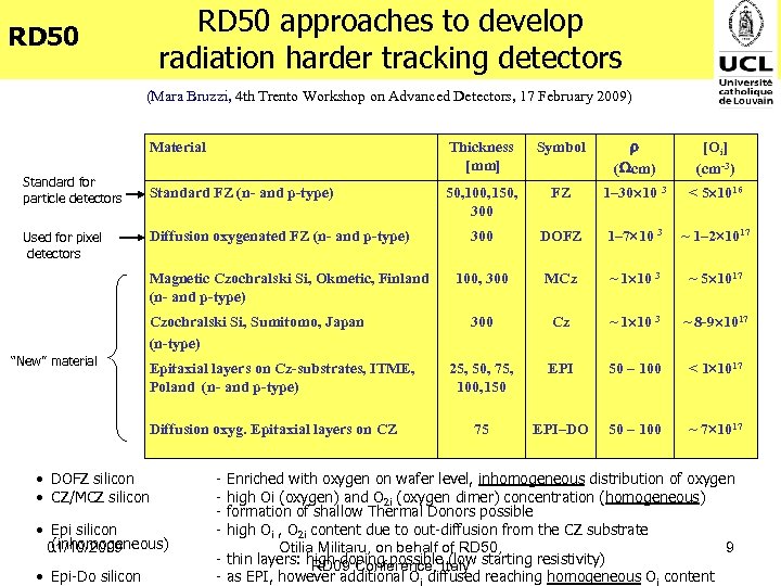 RD 50 approaches to develop radiation harder tracking detectors RD 50 (Mara Bruzzi, 4 th Trento Workshop on Advanced Detectors, 17 February 2009) Material Standard for particle detectors Used for pixel detectors Thickness [mm] Symbol ( cm) [Oi] (cm-3) Standard FZ (n- and p-type) 50, 100, 150, 300 FZ 1– 30 10 3 < 5 1016 300 DOFZ 1– 7 10 3 ~ 1– 2 1017 100, 300 MCz ~ 1 10 3 ~ 5 1017 300 Cz ~ 1 10 3 ~ 8 -9 1017 25, 50, 75, 100, 150 EPI 50 – 100 < 1 1017 75 EPI–DO 50 – 100 ~ 7 1017 Diffusion oxygenated FZ (n- and p-type) Magnetic Czochralski Si, Okmetic, Finland (n- and p-type) Czochralski Si, Sumitomo, Japan (n-type) “New” material Epitaxial layers on Cz-substrates, ITME, Poland (n- and p-type) Diffusion oxyg. Epitaxial layers on CZ • DOFZ silicon • CZ/MCZ silicon • Epi silicon (inhomogeneous) 01/10/2009 • Epi-Do silicon - Enriched with oxygen on wafer level, inhomogeneous distribution of oxygen high Oi (oxygen) and O 2 i (oxygen dimer) concentration (homogeneous) formation of shallow Thermal Donors possible high Oi , O 2 i content due to out-diffusion from the CZ substrate Otilia Militaru, on behalf of RD 50, 9 - thin layers: high doping possible. Italy starting resistivity) (low RD 09 Conference, - as EPI, however additional Oi diffused reaching homogeneous Oi content
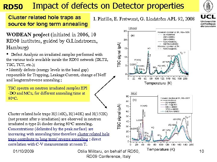 RD 50 Impact of defects on Detector properties Cluster related hole traps as source for long term annealing I. Pintilie, E. Fretwurst, G. Lindström APL 92, 2008 WODEAN project (initiated in 2006, 10 RD 50 institutes, guided by G. Lindstroem, Hamburg) • Defect Analysis on irradiated samples performed with the various tools available inside the RD 50 network (DLTS, TSC, TCT, etc. ); • Identify defects (energy levels in the band gap) responsible for Trapping, Leakage Current, change of Neff and longterm/reverse annealing ; TSC spectra on neutron irradiated samples EPI -DO and MCz, for different annealing time at 80 o. C. Cluster related hole traps H(116 K), H(140 K) and H(152 K) (not present after γ-irradiation) are observed in neutron irradiated n-type Si diodes during 80 o. C annealing. Concentrations (delimited by the peak surface) are increasing with annealing time therefore cluster related hole traps contribute to long term/ reverse annealing ; direct correlation with C-V measurements at room T. 01/10/2009 Otilia Militaru, on behalf of RD 50, RD 09 Conference, Italy 10
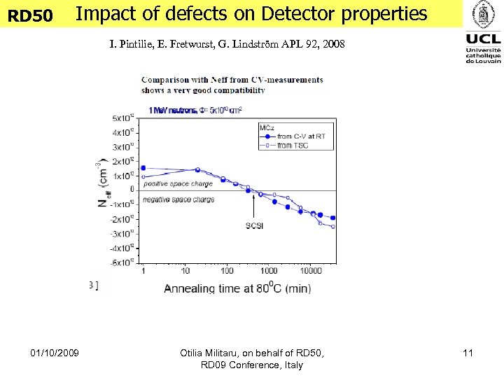 RD 50 Impact of defects on Detector properties I. Pintilie, E. Fretwurst, G. Lindström APL 92, 2008 01/10/2009 Otilia Militaru, on behalf of RD 50, RD 09 Conference, Italy 11
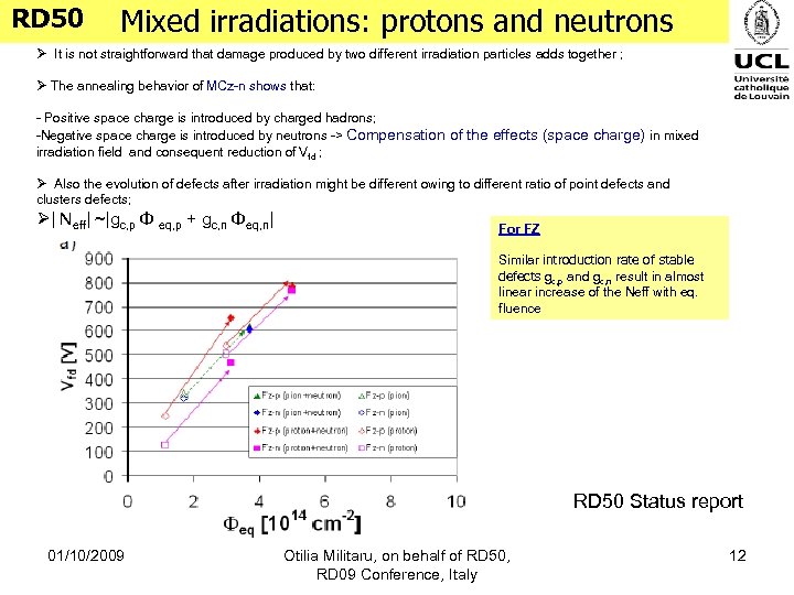 RD 50 Mixed irradiations: protons and neutrons Ø It is not straightforward that damage produced by two different irradiation particles adds together ; Ø The annealing behavior of MCz-n shows that: - Positive space charge is introduced by charged hadrons; -Negative space charge is introduced by neutrons -> Compensation of the effects (space charge) in mixed irradiation field and consequent reduction of Vfd ; Ø Also the evolution of defects after irradiation might be different owing to different ratio of point defects and clusters defects; Ø| Neff| ~|gc, p Φ eq, p + gc, n Φeq, n| For FZ Similar introduction rate of stable defects gc, p and gc, n result in almost linear increase of the Neff with eq. fluence RD 50 Status report 01/10/2009 Otilia Militaru, on behalf of RD 50, RD 09 Conference, Italy 12
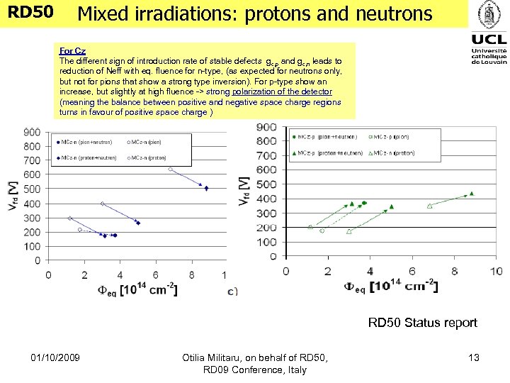 RD 50 Mixed irradiations: protons and neutrons For Cz The different sign of introduction rate of stable defects gc, p and gc, n leads to reduction of Neff with eq. fluence for n-type, (as expected for neutrons only, but not for pions that show a strong type inversion). For p-type show an increase, but slightly at high fluence -> strong polarization of the detector (meaning the balance between positive and negative space charge regions turns in favour of positive space charge ) RD 50 Status report 01/10/2009 Otilia Militaru, on behalf of RD 50, RD 09 Conference, Italy 13
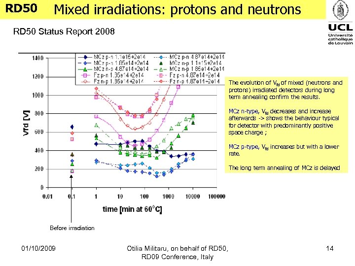 RD 50 Mixed irradiations: protons and neutrons RD 50 Status Report 2008 The evolution of Vfd of mixed (neutrons and protons) irradiated detectors during long term annealing confirm the results. MCz n-type, Vfd decreases and increase afterwards -> shows the behaviour typical for detector with predominantly positive space charge ; MCz p-type, Vfd increases but with a lower rate. The long term annealing of MCz is delayed Before irradiation 01/10/2009 Otilia Militaru, on behalf of RD 50, RD 09 Conference, Italy 14
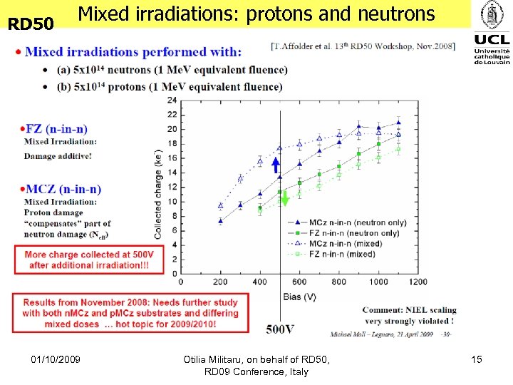 RD 50 Mixed irradiations: protons and neutrons 01/10/2009 Otilia Militaru, on behalf of RD 50, RD 09 Conference, Italy 15
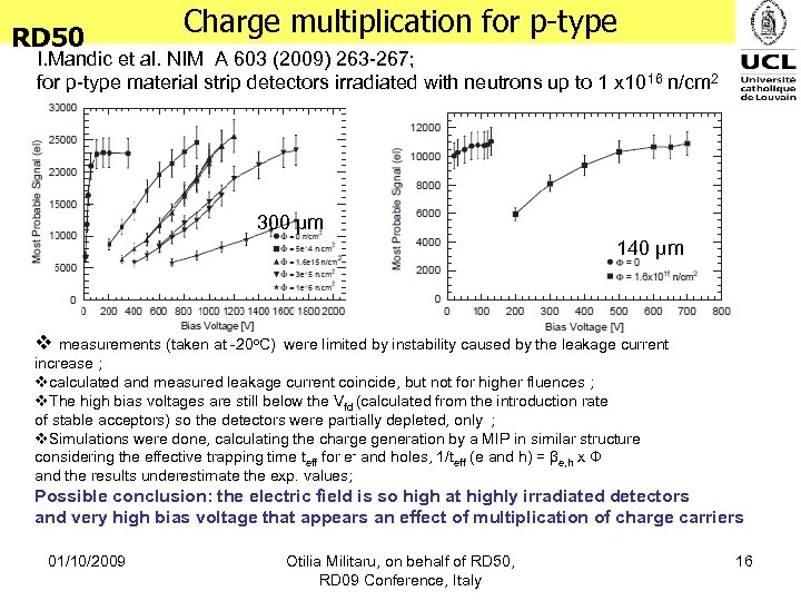 RD 50 Charge multiplication for p-type I. Mandic et al. NIM A 603 (2009) 263 -267; for p-type material strip detectors irradiated with neutrons up to 1 x 10¹⁶ n/cm 2 300 µm 140 µm v measurements (taken at -20 o. C) were limited by instability caused by the leakage current increase ; vcalculated and measured leakage current coincide, but not for higher fluences ; v. The high bias voltages are still below the Vfd (calculated from the introduction rate of stable acceptors) so the detectors were partially depleted, only ; v. Simulations were done, calculating the charge generation by a MIP in similar structure considering the effective trapping time teff for e- and holes, 1/teff (e and h) = βe, h x Φ and the results underestimate the exp. values; Possible conclusion: the electric field is so high at highly irradiated detectors and very high bias voltage that appears an effect of multiplication of charge carriers 01/10/2009 Otilia Militaru, on behalf of RD 50, RD 09 Conference, Italy 16
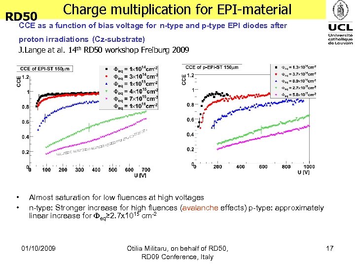 RD 50 Charge multiplication for EPI-material CCE as a function of bias voltage for n-type and p-type EPI diodes after proton irradiations (Cz-substrate) J. Lange at al. 14 th RD 50 workshop Freiburg 2009 • • Almost saturation for low fluences at high voltages n-type: Stronger increase for high fluences (avalanche effects) p-type: approximately linear increase for Feq≥ 2. 7 x 1015 cm-2 01/10/2009 Otilia Militaru, on behalf of RD 50, RD 09 Conference, Italy 17
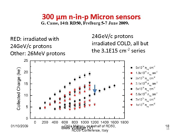 300 µm n-in-p Micron sensors G. Casse, 14 th RD 50, Freiburg 5 -7 June 2009. RED: irradiated with 24 Ge. V/c protons Other: 26 Me. V protons 01/10/2009 24 Ge. V/c protons irradiated COLD, all but the 3. 1 E 15 cm-2 series Otilia Militaru, on behalf of RD 50, RD 09 Conference, Italy 18 18
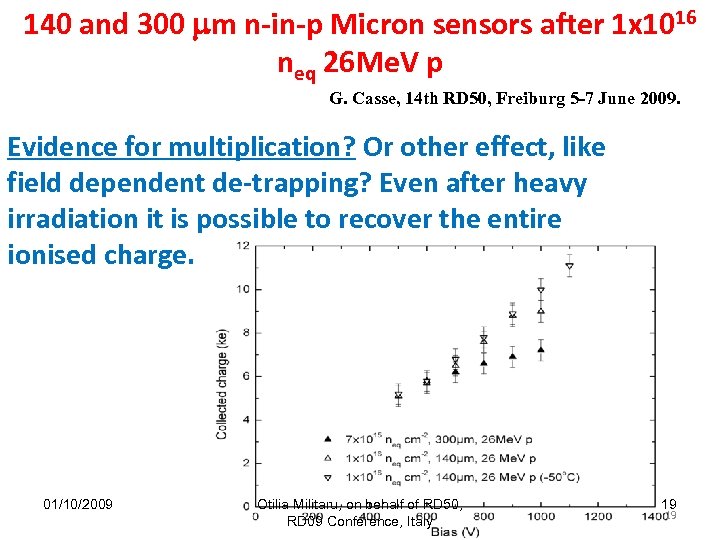 140 and 300 mm n-in-p Micron sensors after 1 x 10¹⁶ neq 26 Me. V p G. Casse, 14 th RD 50, Freiburg 5 -7 June 2009. Evidence for multiplication? Or other effect, like field dependent de-trapping? Even after heavy irradiation it is possible to recover the entire ionised charge. 01/10/2009 Otilia Militaru, on behalf of RD 50, RD 09 Conference, Italy 19 19
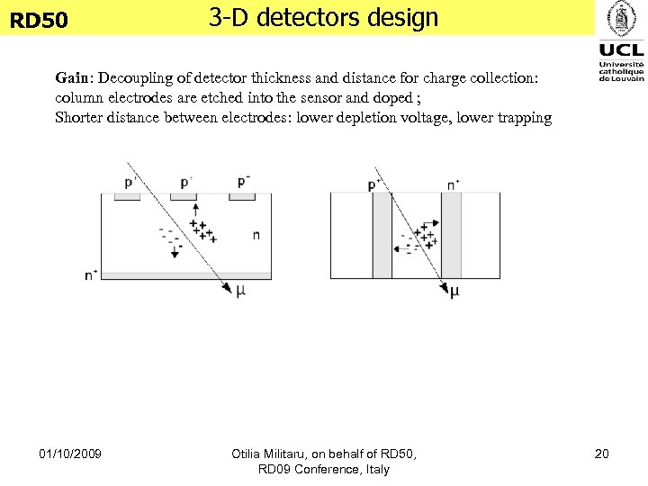 RD 50 3 -D detectors design Gain: Decoupling of detector thickness and distance for charge collection: column electrodes are etched into the sensor and doped ; Shorter distance between electrodes: lower depletion voltage, lower trapping 01/10/2009 Otilia Militaru, on behalf of RD 50, RD 09 Conference, Italy 20
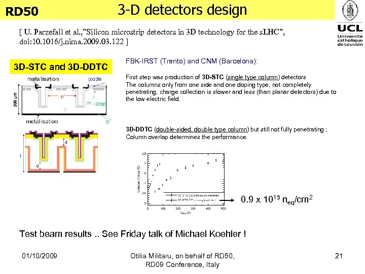 RD 50 3 -D detectors design [ U. Parzefall et al. , ”Silicon microstrip detectors in 3 D technology for the s. LHC”, doi: 10. 1016/j. nima. 2009. 03. 122 ] 3 D-STC and 3 D-DDTC FBK-IRST (Trento) and CNM (Barcelona): First step was production of 3 D-STC (single type column) detectors The columns only from one side and one doping type, not completely penetrating, charge collection is slower and less (than planar detectors) due to the low electric field. 3 D-DDTC (double-sided, double type column) but still not fully penetrating ; Column overlap determines the performance. 0. 9 x 10¹⁵ neq/cm 2 Test beam results. . See Friday talk of Michael Koehler ! 01/10/2009 Otilia Militaru, on behalf of RD 50, RD 09 Conference, Italy 21
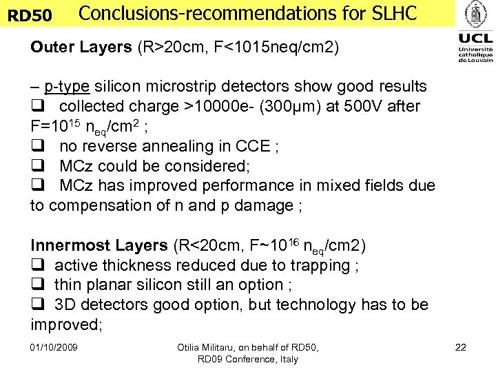 RD 50 Conclusions-recommendations for SLHC Outer Layers (R>20 cm, F<1015 neq/cm 2) – p-type silicon microstrip detectors show good results q collected charge >10000 e- (300μm) at 500 V after F=1015 neq/cm 2 ; q no reverse annealing in CCE ; q MCz could be considered; q MCz has improved performance in mixed fields due to compensation of n and p damage ; Innermost Layers (R<20 cm, F~1016 neq/cm 2) q active thickness reduced due to trapping ; q thin planar silicon still an option ; q 3 D detectors good option, but technology has to be improved; 01/10/2009 Otilia Militaru, on behalf of RD 50, RD 09 Conference, Italy 22


