e1976934570203822c6745dff8ca34e6.ppt
- Количество слайдов: 71


8255 A Programmable Peripheral Interface

Introduction 8255 A is one of the mostly used programmable, Parallel I/O device. It can be used to transfer the data on various conditions When ever multiple I/O ports are required, 8255 A is used for flexible interfacing between MPU and I/O peripherals

Introduction 3 MPU interface to external devices through both parallel and serial interfaces. Parallel data occur in system that use: Displays Keyboard Printers (old printer) Etc. Serial data occurs in: Some printers Data communications

About 24 I/O pins 8 bit parallel ports: A, B C port: can be grouped as 4 bit CU(C upper) and CL(C Lower) Two Modes: BSR(Bit Set/reset) and I/O mode BSR mode set/reset in port C I/O mode is further divided in 3 modes: Mode 0: simple Mode 1: Handshake Mode 2 : Bidirectional

Pin Diagram

Pin diagram of 8255 A
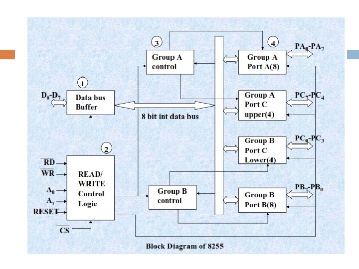

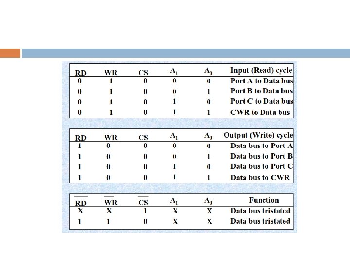
PIN Description 8255 A is having 24 I/O pins This 24 are divided in 3, 8 -bit ports(A, B, C) Port C can be used as individual pins or it can be grouped in 2, 4 -bits port (C-upper, C-lower) The functions of this port A, B, C is been written on Control register. RD(AL): When this signal is low, MPU reads data from selected I/O port WR(AL): When this signal is low, MPU Writes the data into selected I/O port or Control Register Reset : It is active high signal, it clears the bits in control register and sets all port into I/P mode.
 is")
Port address is determined to pins Ao and A 1. CS (AL) is been used to select the 8255 A If A 7=1, and A 6 -A 2=0. Ports will be having the address from 80 H to 83 H

8255 A Programmable Peripheral interfacing

Control Register

Modes in 8255 A is having 2 types of operating modes Bit SET/RESET mode : - Used to set and reset the bits in port C only This mode will be selected when D 7 bit of control register is “ 0”. I/O mode: used to transfer the data. This mode is selected when D 7 bit of control register is set to “ 1” Divided into 3 types Mode 0: All ports will function as simple I/O ports Mode 1: Hand shake Mode 2: Port A can be SET for bidirectional data transfer using handshake mechanism with port c, and Port B can be used either Mode 0 or 1.
 In this mode each line of port C(PC 0 -PC 7)")
Bit SET/RESET (BSR) In this mode each line of port C(PC 0 -PC 7) can SET/RESET by suitably loading the control word register.

Example As an example, if it is needed that PC 5 be set, then in the control word, Since it is BSR mode, D 7 = '0'. Since D 4, D 5, D 6 are not used, assume them to be '0'. PC 5 has to be selected, hence, D 3 = '1', D 2 = '0', D 1 = '1'. PC 5 has to be set, hence, D 0 = '1'. Thus, as per the above values, 0 B (Hex) will be loaded into the Control Word Register (CWR).

I/O mode

Steps for data receiving or transferring to peripheral Mode 0 – input mode In the input mode, the 8255 gets data from the external peripheral ports and the CPU reads the received data via its data bus. The CPU first selects the 8255 chip by making CS low. It then selects the desired port using A 0 and A 1 lines. The CPU then issues an RD signal to read the data from the external peripheral device via the system data bus. Mode 0 - Output mode In the output mode, the CPU sends data to 8255 via system data bus and then the external peripheral ports receive this data via 8255 port. CPU first selects the 8255 chip by making CS low. It then selects the desired port using A 0 and A 1 lines. CPU then issues a WR signal to write data to the selected port via the system data bus. This data is then received by the external peripheral device connected to the selected port.

8255 A Programmable Peripheral Interface 18 Mode 0: Input / Output Mode In this mode port A and B use 8 -bit I/O data and port C uses two ports 4 -bit data. The characteristics of mode 0 are: Output is latched. Input does not latched. Ports do not have the capability of handshake mode or interrupt mode.

Example : Figure 9: 19

8255 PIA: Example Solutions: Port Address : It is actually an I/O memory map. When A 15 is active high, Chip Select signal is activated. Assuming all don’t care signals are at logic 0, therefore ports’ address are as follows: 20

8255 A Programmable Peripheral Interface Solution: Control Word: 21

8255 PIA: BSR Mode Example: Write a BSR control word subroutine to set bit PC 7 and PC 3, and reset after 10 ms. Use the schematic diagram as shown below. 22

8255 A Programmable Peripheral Interface Solution: BSR Control Word: Port Address: • As shown in previous example : 83 H 23

8255 A Programmable Peripheral Interface Solution: Subroutine: Assuming that the delay subroutine has been determined earlier. 24

Example Write a program to read the DIP switches and display the reading from port B at port A and from Cl at port Cu. Consider Port A=8000 h(A 1=0, A 0=0) Port B=8001 H(A 1=0, A 0=1) Port C= 8002 H(A 1=1, A 0=0) Control register=8003 H(A 1=1, A 0=1).

Control word D 7=1, I/O function D 6, D 5=00 PORT A in MODE 0 D 4=0, Port A=OUTPUT D 3=0, Port Cu=OUTPUT D 2=0, PORT B in mode 0 D 1=1, port B=input D 0=1, port Cl=Input.

MVI A, 83 H; load accumulator with the control word STA 8003 H; write the word in the control register to initialize the ports LDA 8001 H; Read the switches at port B STA 8000 H; Display the reading at port A LDA 8002 H; Read switches at port C ANI 0 FH; mask the upper four bits of port c. these bits are not input data RLC RLC STA 8002 H, Display data at port Cl HLT
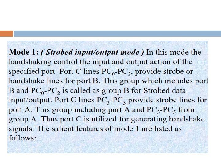
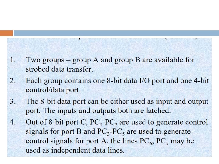

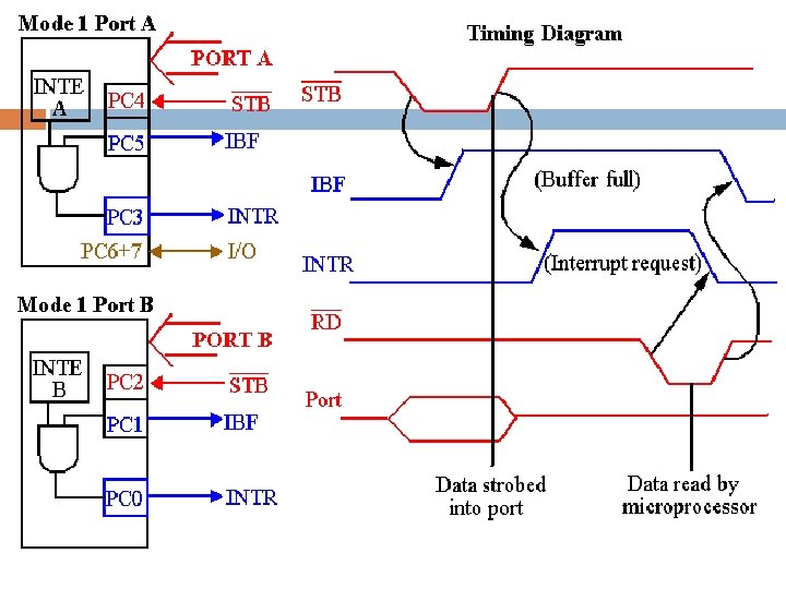
Mode 1 • • This mode is same as mode 0 but only difference is port C is been used for handshaking and control. Two ports i. e. port A and Port B can be used as 8 bit i/o port Each port uses 3 lines of the port C as handshake signals and remaining two signals can be function as i/o port Interrupt logic is supported.
 • • Strobe input(STB(AL)): This is generated by peripheral device")
Input control signals(handshaking signal) • • Strobe input(STB(AL)): This is generated by peripheral device to indicate that it has transmitted a byte of data. In response to STB, 8255 generates IBF and INTR signals IBF (Input Buffer Full): This indicate that input latch has received the data byte. It acknowledgement signal by 8255. INTR(Interrupt Request): This is an o/p signal that is used as interrupt to MPU. INTE( Interrupt Enable): This internal flip-flop , which is been used to enable or disable the generation of INTR signal.

Mode 1 Input

Input configuration

Input mode configuration
")
Timing diagram for strobed input(with handshake)

Output configuration

Output configuration

Timing waveforms for output configuration
 Find port addresses")
Application of MODE 1( Keyboard as input and output as printer) Find port addresses by analyzing the decode logic Determine the control word to setup port A as input and port B as output in mode 1 Determine the BSR word to enable INTEa(port A) Determine the masking byte to verify the OBFb(AL) line in the status check I/O(PORT) Write initialization instructions and printer subroutine to output characters that are stored in memory

LED Display for Binary data

Instruction to display on LED DISPLAY MVI A, DATA; load accumulator with data OUT FFH; output accumulator contents to port FFH HLT ; end the program


Mode 1: Input or Output with Handshake o In this mode, handshake signals are exchanged between the MPU and peripherals prior to data transfer.

Mode 1: Input or Output with Handshake The features of the mode include the following: o Two ports (A and B) function as 8 -bit I/O ports. o They (A and B) can be configured as either as input or output ports. o Each port uses three lines from Port C as handshake signals. o The remaining two lines of Port C can be used for simple I/O operations. o Input and Output data are latched. o Interrupt logic is supported.

Mode 1 Input
 : generated by peripheral to indicate it")
Signal Description STB- Strobe input: (active low) : generated by peripheral to indicate it has transmitted the data. IBF( Input buffer full) : Acknowledged by 8255 to indicate the input buffer has received the data. INTR( Interrupt Request) : This is output signal that is used to INTR the u. P. This is high when STB , IBF and INTE(internal signal) is high. INTE (Interrupt Enable): internal flip flop

Control Word and Status Word

82 C 55 : Mode 1 Output Exam.

Control and Status Word

Mode 2: Bidirectional Data Transfer This mode is used primarily in applications such as data transfer between two computers. In this mode, Port A can be configured as the bidirectional port and Port B either in Mode 0 or Mode 1.

Mode 2: Bidirectional Data Transfer Port A uses five signals from Port C as handshake signals for data transfer. The remaining three signals from port C can be used either as simple I/O or as handshake for port B.

8255: Mode 2 Bi-directional Operation “Handshaking” signals are provided to maintain proper bus flow discipline in a similar manner to MODE 1. Interrupt generation and enable/disable functions are also available.

MODE 2 Basic Functional Definitions: Used in Group A only. One 8 -bit, bi-directional bus port (Port A) and a 5 -bit control port (Port C). Both inputs and outputs are latched.

8255: Mode 2 Bi-directional Operation • Timing diagram is a combination of the Mode 1 Strobed Input and Mode 1 Strobed Output Timing diagrams.

8255: Mode 2 Bi-directional Operation INTR : Interrupt request is an output that requests an interrupt. ~OBF : Output Buffer Full is an output indicating that output buffer contains data for the bi-directional bus. ~ACK : Acknowledge is an input that enables tri-state buffers which are otherwise in their high-impedance state. ~STB : The strobe input loads data into the port A latch.

8255: Mode 2 Bi-directional Operation IBF : Input buffer full is an output indicating that the input latch contains information for the external bidirectional bus. INTE : Interrupt enable are internal bits that enable the INTR pin. BIT PC 6(INTE 1) and PC 4(INTE 2). PC 2, PC 1, PC 0 : These port C pins are generalpurpose I/O pins that are available for any purpose.

Mode 2 Timing Diagram

Write a program to initialize 8255 in the configuration given below: 1. Port A: Simple input 2. Port B: Simple output 3. Port CL: Output 4. Port Cu: Input

Write a program to initialize 8255 in the configuration given below: 1. Port A: Simple input 2. Port B: Simple output 3. Port CL: Output 4. Port Cu: Input Assume address of the control word register of 8255 as 83 H. Solution: MVI A, 98 H : Load control word OUT 83 H : Send control word

Write a program to initialize 8255 in the configuration given below: 1. Port A: Output with handshake 2. Port B: Input with handshake 3. Port CL: Output 4. Port Cu: Input

Write a program to initialize 8255 in the configuration given below: 1. Port A: Output with handshake 2. Port B: Input with handshake 3. Port CL: Output 4. Port Cu: Input Assume address of the control word register of 8255 as 83 H. MVI A, AEH : Load control word OUT 83 H : Send control word

Interface an 8 -digit 7 segment LED display using 8255 to the 8085 microprocessor system and write an 8085 assembly language routine to display message on the display.
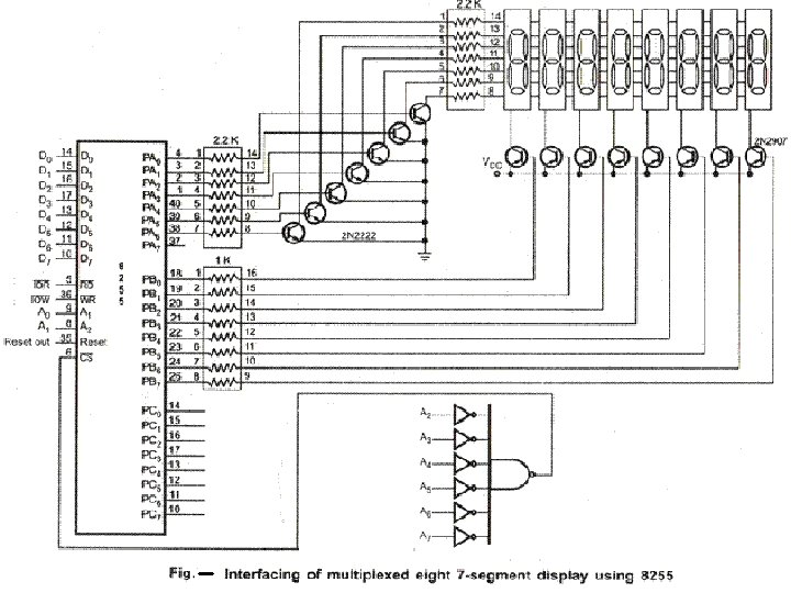

port A and port B are used as simple latched output ports. Port A provides the segment data inputs to the display and port B provides a means of selecting a display position A 0 -A 7 lines are used to decode the addresses for 8255. For this circuit different addresses are: PA = 00 H PB = 01 H PC = 02 H CR = 03 H.

Source program: SOFTWARE TO INITIALIZE 8255: MVI A, 80 H : Load control word in AL OUT CR : Load control word in CR SUBROUTINE TO DISPLAY MESSAGE ON MULTIPLEXED LED DISPLAY: SET UP REGISTERS FOR DISPLAY: MVI B, 08 H : load count MVI C, 7 FH : load select pattern (for selecting one of the digit) LXI H, 6000 H : starting address of message DISPLAY MESSAGE: DISP 1: MOV A, C : select digit OUT PB MOV A, M : get data OUT PA : display data CALL DELAY : wait for some time MOV A, C : MOV A, C RRC (right rotate for selecting second digit) MOV C, A : adjust selection pattern INX H DCR B : Decrement count JNZ DISP 1 : repeat 8 times RET

CODE CONVERSION

Convert a 2 -digit BCD number stored at memory address 2200 H into its binary equivalent number and store the result in a memory location 2300 H.
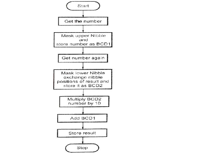

Convert a 2 -digit BCD number stored at memory address 2200 H into its binary equivalent number and store the result in a memory location 2300 H. Sample problem 1: LDA 2200 H : Get the BCD number (2200 H) = 67 H MOV B, A : Save it (2300 H) = 6 x OAH + 7 = 3 CH + 7 = ANI OFH : Mask most significant four bits MOV C, A : Save unpacked BCDI in C register 43 H MOV A, B : Get BCD again ANI FOH : Mask least significant four bits RRC : Convert most significant four bits into unpacked BCD 2 RRC RRC MOV B, A : Save unpacked BCD 2 in B register XRA A : Clear accumulator (sum = 0) MVI D, 0 AH : Set D as a multiplier of 10 Sum: ADD D : Add 10 until (B) = 0 DCR B : Decrement BCD 2 by one JNZ SUM : Is multiplication complete? i if not, go back and add again ADD C : Add BCD 1 STA 2300 H : Store the result HLT : Terminate program execution

e1976934570203822c6745dff8ca34e6.ppt