
30. 01. 16 11 Processes for Micromachining The

processes_for_micromachining-lecture_1.ppt
- Размер: 512 Кб
- Количество слайдов: 36
Описание презентации 30. 01. 16 11 Processes for Micromachining The по слайдам
30. 01. 16 11 Processes for Micromachining The methods used in the fabrication of MEMS. — Micromachining is a parallel (batch) process in which dozens to tens of thousands of identical elements are fabricated simultaneously on the same wafer. — Another key difference is the minimum feature dimension—on the order of one micromete r —which is an order of magnitude smaller than what can be achieved using conventional machining. The technological toolbox consists of three major categories: basic, advanced, and non-lithographic processes.
30. 01. 16 22 The nonlithographic processes are more conventional means of producing microstructures, which may be combined with other processes to produce a final MEMS product. The basic process tools are well-established methods and are usually available at major foundry facilities. The advanced process tools are unique in their nature and are normally limited to a few specialized facilities. For example: LIGA, a micromachining process using electroplating and molding. LIGA is a German acronym for lithographie, galvanoformung, und abformung, meaning lithography, electroplating, and molding. Lecture
30. 01. 16 33. Silicon micromachining combines adding layers of material over a silicon wafer with etching (selectively removing material) precise patterns in these layers or in the underlying substrate. The implementation ( реализация) is based on a broad portfolio of fabrication processes, including material deposition, patterning, and etching techniques. Lithography plays a significant role in the delineation ( формирование рисунка) of accurate and precise patterns. .
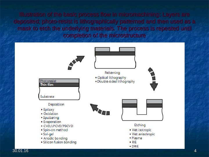
Illustration of the basic process flow in micromachining: Layers are deposited; photo-resist is lithographically patterned and then used as a mask to etch the underlying materials. The process is repeated until completion of the microstructure 30. 01.
30. 01. 16 55 Basic Process Tools Epitaxy, sputtering, evaporation, chemical-vapor deposition, and spin-on methods are common techniques used to deposit uniform layers of semiconductors, metals, insulators, and polymers. Lithography is a photographic process for printing images onto a layer of photosensitive polymer (photoresist) that is subsequently used as a protective mask against etching. Wet and dry etching, including deep reactive ion etching , form the essential process base to selectively remove material.
30. 01. 16 66 Epitaxy is a deposition method to grow a crystalline silicon layer over a silicon wafer, but with a differing dopant type and concentration. The epitaxial layer is typically 1 to 20 µm thick. It exhibits the same crystal orientation as the underlying crystalline substrate, except when grown over an amorphous material (e. g. , a layer of silicon dioxide), it is polycrystalline.
30. 01. 16 77 The growth occurs in a vapor-phase chemical-deposition reactor from the dissociation or hydrogen reduction at high temperature (>800ºC) of a silicon-containing source gas. Common source gases are silane (Si. H 44 ), ), dichlorosilane (Si. H 22 Cl. Cl 22 ), ), or or silicon tetrachloride (Si. Cl 44 ). ). Nominal growth rates are between 0. 2 and 4 µm/min , depending on the source gas and the growth temperature. Epitaxy
30. 01. 16 88 Epitaxy Impurity dopants are simultaneously incorporated during growth by the dissociation of a dopant source gas in the same reactor. Arsine (As. H 33 )) and phosphine (PH(PH 33 ), ), two extremely toxic gases , are used for arsenic and phosphorous (n-type) doping. Diborane (B 22 HH 66 )) is used for boron (p-type) doping.
Epitaxy can be used to grow crystalline silicon on other types of crystalline substrates such as sapphire (Al(Al 22 OO 33 ). ). The process is called heteroepitaxy to to indicate the difference in materials. Silicon-on-sapphire (SOS) wafers are available from a number of vendors and are effective in applications where an insulating or a transparent substrate is is required. The lattice mismatch between the sapphire and silicon crystals limits the thickness of the silicon to about one micrometer. Thicker silicon films suffer from (страдают от) high defect densities and degraded electronic performance 30. 01.
30. 01. 16 1010 Oxidation High-quality amorphous silicon dioxide is obtained by oxidizing silicon in either dry oxygen or in steam at elevated temperatures (850º– 1, 150ºC). Oxidation mechanisms have been extensively studied and are well understood. Charts showing final oxide thickness as function of temperature, oxidizing environment, and time are widely available.
30. 01. 16 1111 Oxidation Thermal oxidation of silicon generates compressive stress in the silicon dioxide film. There are two reasons for the stress: 11. . Silicon dioxide molecules take more volume than silicon atoms. 2. 2. There is a mismatch between the coefficients of thermal expansion of silicon and silicon dioxide. Te(Si) = 2. 6µm/(m·K) (at 25°C); Te(Si. O 2) = 5. 610 E-7 1/K
The compressive stress depends on the total thickness of the silicon dioxide layer and can reach hundreds of MPa. As a result, thermally grown oxide films cause bowing (прогиб) of the underlying substrate. Moreover, freestanding membranes and suspended cantilevers made of thermally grown silicon oxide tend to warp (( коробиться) or curl (скручиваться) due to stress variation through the thickness of the film. 30. 01.
30. 01. 16 1313 Sputter Deposition In sputter deposition, a target made of a material to be deposited is physically bombarded by a flux of inert-gas ions (usually argon) in a vacuum chamber at a pressure of 0. 1– 10 Pa. Atoms or molecules from the target are ejected and deposited onto the wafer. There are several general classes of sputter tools differing by the ion excitation mechanism. In direct-current (DC) glow discharge, suitable only for electrically conducting materials , the inert-gas ions are accelerated in a DC electric field between the target and the wafer. In planar RF, the target and the wafer form two parallel plates with RF excitation applied to the target, suitable for dielectric materials. In ion-beam deposition (also known as ion milling), ions are generated in a remote plasma, then accelerated at the target. Basic Process Tools 35 RF planar sputtering and ion-beam methods work for the deposition of both conducting and insulating materials, such as silicon dioxide.
30. 01. 16 1414 Sputter Deposition In In planar and cylindrical magnetron sputtering, an externally applied magnetic field increases the ion density near the target, thus raising the deposition rates. Typical deposition rates are 0. 1– 0. 3 µm/min , and can be as high as 1 µm/min for aluminum in certain sputtering tools.
30. 01. 16 1515 Sputter Deposition Nearly any inorganic material can be sputtered. Sputtering is a favored method in the MEMS community for the deposition at low temperatures (<150ºC) of thin metal films such as aluminum, titanium, chromium, platinum, palladium, tungsten, Al/Si and Ti/W alloys, amorphous silicon, insulators including glass, and piezoelectric ceramics (e. g. , PZT [[ Lead Zirconate Titanate (piezoelectric ceramic material) ]] and Zn. O ). ). In a variation known as reactive sputtering, a reactive gas such as nitrogen or oxygen is added during the sputtering of a metal to form compounds such as titanium nitride or titanium dioxide. .
30. 01. 16 1616 Sputter Deposition The directional randomness of the sputtering process, provided that the target size is larger than the wafer, results in good step coverage—the uniformity of the thin film over a geometrical step—though some thinning occurs near corners. The deposited film has a very fine granular structure and is usually under stress. The stress levels vary with the sputter power and chamber pressure during deposition, with tensile stress occurring at lower power and higher pressure , and compressive stress occurring at higher power and lower pressure. The transition between the compressive and tensile regimes is often sharp (over a few tenths of a Pa), making the crossover—an ideal point for zero-stress deposition—difficult to control. Heating the substrate during deposition is sometimes used to reduce film stress.
30. 01. 16 1717 Sputter Deposition Many metals, particularly inert ones such as gold, silver, and platinum , do not adhere well to silicon, silicon dioxide, or silicon nitride , peeling off (снимаются) immediately after deposition or during later handling. A thin (5 — to 20 -nm) adhesion layer, which bonds to both the underlying material and the metal over it, enables the inert metal to stick. The most common adhesion layers are Cr, Ti, and Ti/W alloy. The inert metal must be deposited on the adhesion layer without breaking the vacuum, as oxygen in the air would immediately oxidize the adhesion layer, rendering it useless.
30. 01. 16 1818 Evaporation involves the heating of a source material to a high temperature, generating a vapor that condenses on a substrate to form a film. Nearly any element (e. g. , Al, Si, Ti, Au), including many high-melting-point refractory (тугоплавкий ) ) metals and compounds (e. g. , Cr, Mo, Ta, Pd, Pt, Ni/Cr, Al 22 OO 33 ), can be evaporated. Deposited films comprised of more than one element may not have the same composition as the source material because the evaporation rates may not correspond to the stoichiometry of the source.
30. 01. 16 1919 Evaporation is performed in a vacuum chamber with the background pressure typically below 10− 4 Pa to to avoid contaminating the film. Target heating can be done resistively by passing an electrical current through a tungsten filament, strip, or boat holding the desired material. Heating can alternatively be done by scanning a high-voltage (e. g. , 10 -k. V) electron beam (e-beam) over the source material. In this case, the carrier is usually made of tungsten, graphite, alumina, or copper (copper is an excellent thermal conductor, but it can only be used if it is not wetted by the molten source). .
30. 01. 16 2020 Evaporation Resistive evaporation is simple but can result in spreading impurities or other contaminants present in the filament. E-beam evaporation, by contrast, can provide better-quality films and slightly higher deposition rates (5– 100 nm/min), but the deposition system is more complex, requiring water cooling of the target and shielding from x-rays generated when the energetic electrons strike the target. Furthermore, radiation that penetrates the surface of the silicon substrate during the deposition process can damage the crystal and degrade the characteristics of electronic circuits.
30. 01. 16 2121 Evaporation is a directional deposition process from a relatively small source. This results in the majority of material particles being deposited at a specific angle to the substrate, causing poor step coverage and leaving corners and sidewalls exposed. This is generally an undesirable effect if thin film continuity is desired (e. g. , when the metal is an electrical interconnect).
30. 01. 16 2222 Evaporation Rotating the substrate to face the source at different angles during deposition reduces the effect. In some cases, however, shadowing can be used deliberately to selectively deposit material on one side of a step or a trench but not the other. Thin films deposited by evaporation tend to exhibit tensile stress , increasing with higher material melting point. Evaporated niobium and platinum films, for example, can have tensile stress in excess of 1 GPa , sufficient to cause curling of the wafer or even peeling. As with sputtering, an adhesion layer must be used with many metals.
30. 01. 16 2323 Chemical-Vapor Deposition In contrast to sputtering, CVD is a high-temperature process, usually performed above 300ºC. The field of CVD has grown substantially, driven by the demand within the semiconductor industry for high-quality, thin dielectric and metal films for multilayer electrical interconnects. Common thin films deposited by CVD include polysilicon, silicon oxides and nitrides, tungsten, titanium and tantalum as well as their nitrides, and, most recently, copper and low-permittivity dielectric insulators (ε rr < 3). The latter two are becoming workhorse materials for very-high-speed electrical interconnects in integrated circuits. The deposition of polysilicon, silicon oxides, and nitrides is routine within the MEMS industry.
30. 01. 16 2424 Chemical-Vapor Deposition Chemical vapor deposition processes are categorized as a tmospheric-pressure (referred to as as APCVD ), or low-pressure (LPCVD) , or plasma-enhanced (PECVD)**, which also encompasses high-density plasma (HDP-CVD). APCVD and LPCVD methods operate at rather elevated temperatures (400º– 800ºC). In In PECVD and HDP-CVD , the substrate temperature is typically near 300ºC , though the plasma deposition of silicon nitrides at room temperature is feasible. The effect of deposition parameters on the characteristics of the thin film is significant, especially for silicon oxides and nitrides.
30. 01. 16 2525 Chemical-Vapor Deposition Substrate temperature, gas flows, presence of dopants, and pressure are important process variables for all types of CVD. Power and plasma excitation RF frequency are also important for PECVD. **Energetic electrons excited in a high-frequency electromagnetic field collide with gas molecules to form ions and reactive neutral species. The mixture of electrons, ions, and neutrals is called plasma and constitutes a phase of matter distinct from solids, liquids, or gases. Plasma-phase operation increases the density of ions and neutral species that can participate in a chemical reaction, be it deposition or etching, and thus can accelerate the reaction rate.
30. 01. 16 2626 Deposition of Polysilicon Chemical-vapor deposition processes allow the deposition of polysilicon as a thin film on a silicon substrate. The film thickness can range between a few tens of nanometers to several micrometers. Structures with several layers of polysilicon are feasible. The ease of depositing polysilicon, a material sharing many of the properties of bulk silicon, makes it an extremely attractive material in surface micromachining.
30. 01. 16 2727 Deposition of Polysilicon is deposited by the pyrolysis of silane (Si. H 44 ) to silicon and hydrogen in a LPCVD reactor. Deposition from silane in a low-temperature PECVD reactor is also possible but results in amorphous silicon. The deposition temperature in LPCVD, typically between 550º and 700ºC, affects the granular structure of the film. Below about 600ºC, the thin film is completely amorphous; above about 630ºC, it exhibits a crystalline grain structure. The deposition rate varies from approximately 6 nm/min at 620ºC up to 70 nm/min at 700ºC. Partial pressure and flow rate of the silane gas also affect the deposition rate.
30. 01. 16 2828 Deposition of Polysilicon LPCVD polysilicon films conform well to the underlying topography on the wafer, showing good step coverage. In deep trenches with aspect ratios (ratio of depth to width) in excess of 10, some thinning of the film occurs on the sidewalls, but that has not limited using polysilicon to fill trenches as deep as 500 µm.
30. 01. 16 2929 Deposition of Polysilicon can be doped during deposition—Polysilicon can be doped during deposition— known as in situ doping —by introducing dopant source gases, in particular arsine or phosphine for n-type doping and diborane for p-type doping. Arsine and phosphine greatly decrease the deposition rate (to about one third that of undoped polysilicon), whereas diborane increases it. The dopant concentration in in-situ doped films is normally very high (~10 2020 cm cm − 3− 3 ), ), but the film resistivity remains in the range of 1 to 10 mΩ • cm because of the low mobility of electrons or holes.
30. 01. 16 3030 Deposition of Polysilicon Intrinsic stresses in as-deposited doped polysilicon films can be large (>500 MPa) and either tensile or compressive, depending on the deposition temperature. Furthermore, there is normally a stress gradient through the thickness of the film, which results in curling of released micromechanical structures. Annealing at 900ºC or above causes stress relaxation through structural changes in grain boundaries and a reduction in stress to levels (<50 MPa) and stress gradient generally deemed (считается) acceptable for micromachined structures.
30. 01. 16 3131 Deposition of Silicon Dioxide Silicon dioxide is deposited below 500ºC by reacting silane and oxygen in an APCVD, LPCVD, or PECVD reactor. Due to the low temperature compared to thermally grown oxide, this is known as low-temperature oxide (LTO). The optional addition of phosphine or diborane dopes the silicon oxide with phosphorus or boron, respectively.
30. 01. 16 3232 Deposition of Silicon Dioxide Films doped with phosphorus are often referred to as phos-phosilicate glass (PSG); those doped with phosphorus and boron are known as as borophosphosilicate glass (BPSG). When annealed at temperatures near 1000ºC , both PSG and BPSG soften and flow to conform with the underlying surface topography and to improve step coverage. LTO films are used for passivation coatings over aluminum, but the deposition temperature must remain below about 400ºC to prevent degradation of the metal.
30. 01. 16 3333 Deposition of Silicon Dioxide Silicon dioxide can also be deposited at temperatures between 650º and 750ºC in a LPCVD reactor by the pyrolysis of tetraethoxysilane [Si(OC 22 HH 44 )) 44 ], ], also known as TEOS. Silicon dioxide layers deposited from a TEOS source exhibit excellent uniformity and step coverage , but the high temperature process precludes their use over aluminum. высокотемпературный способ препятствует их использованию по алюминию. A third, but less common, method to deposit silicon dioxide involves reacting dichlorosilane (Si. Cl 22 HH 22 ) ) with nitrous oxide (N(N 22 O) O) in a LPCVD reactor at temperatures near 900ºC. Film properties and uniformity are excellent, but its use is limited to depositing insulating layers over polysilicon
30. 01. 16 3434 Deposition of Silicon Dioxide As is the case for the LPCVD of polysilicon, deposition rates for silicon dioxide increase with temperature. A A typical LTO deposition rate at low pressure is 25 nm/min at 400ºC, rising to 150 nm/min at atmospheric pressure and 450ºC. The deposition rate using TEOS varies from 5 nm/min at 650ºC up to 50 nm/min at 750ºC.
30. 01. 16 3535 Deposition of Silicon Dioxide Deposited silicon dioxide films are amorphous with a structure similar to fused silica. . Heat treatment (annealing) at elevated temperatures (600º– 1, 000ºC) results in the outgassing of hydrogen incorporated in the film and a slight increase in density, but no change in the amorphous structure. This process is called densification.
30. 01. 16 3636 Deposition of Silicon Dioxide Silicon dioxide deposited using CVD methods is very useful as a dielectric insulator between layers of metal or as a sacrificial layer (etched using hydrofluoric acid) in surface micromachining. However, its electric properties are inferior to those of thermally grown silicon dioxide. For example, dielectric strength of CVD silicon oxides can be half that of thermally grown silicon dioxide. It is no coincidence that gate insulators for CMOS transistors are made of the latter type. In general, CVD silicon oxides are under compressive stress (100– 300 MPa). The stress cannot be controlled except when PECVD is used.