
30. 01. 16 11 Lecture 3 Etching


- Размер: 1.7 Mегабайта
- Количество слайдов: 34
Описание презентации 30. 01. 16 11 Lecture 3 Etching по слайдам
30. 01. 16 11 Lecture 3 Etching
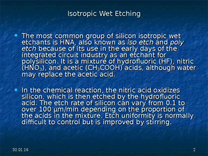
30. 01. 16 22 Isotropic Wet Etching The most common group of silicon isotropic wet etchants is HNA, also known as isoiso etch and poly etch because of its use in the early days of the integrated circuit industry as an etchant for polysilicon. It is a mixture of hydrofluoric (HF), nitric (HNO 33 ), and acetic (CH(CH 33 COOH) acids, although water may replace the acetic acid. In the chemical reaction, the nitric acid oxidizes silicon, which is then etched by the hydrofluoric acid. The etch rate of silicon can vary from 0. 1 to over 100 µm/min depending on the proportion of the acids in the mixture. Etch uniformity is normally difficult to control but is improved by stirring.
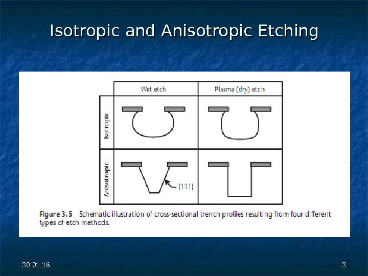
30. 01. 16 33 Isotropic and Anisotropic Etching
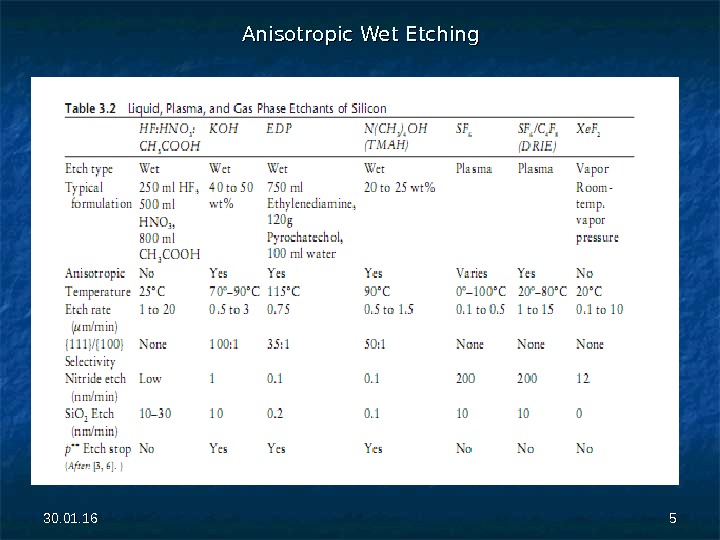
30. 01. 16 44 Anisotropic wet etchants are also known as orientation-dependent etchants (ODEs) because their etch rates depend on the crystallographic direction. The list of anisotropic wet etchants includes the hydroxides of alkali metals (e. g. , Na. OH, KOH, Cs. OH), simple and quaternary ammonium hydroxides (e. g. , NHNH 44 OH, N(CH 33 )) 44 OH), and ethylenediamine mixed with pyrochatechol (EDP) in water. . The solutions are typically heated to 70º– 100ºC. A comparison of various silicon etchants is given in Table 3. 2.
30. 01. 16 55 Anisotropic Wet Etching
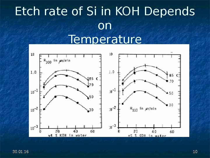
30. 01. 16 66 KOH is by far the most common ODE Etch rates are typically given in the [100] direction, corresponding to the etch front being the (100) plane. The {110} planes are etched in KOH about twice as rapidly as {100} planes. While {111} planes are etched at a rate about 100 times slower than for {100} planes.
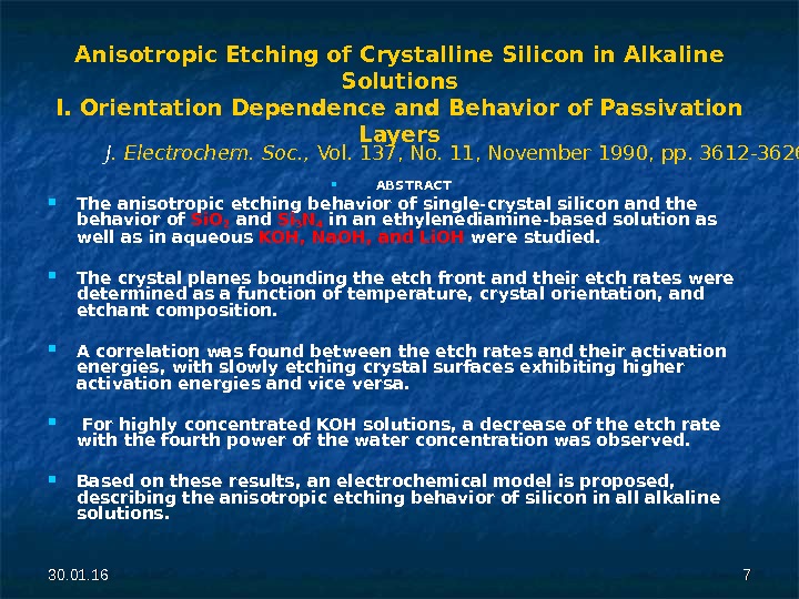
30. 01. 16 77 Anisotropic Etching of Crystalline Silicon in Alkaline Solutions I. Orientation Dependence and Behavior of Passivation Layers ABSTRACT The anisotropic etching behavior of single-crystal silicon and the behavior of Si. O 2 and Si 3 N 4 in an ethylenediamine — based solution as well as in aqueous KOH, Na. OH, and Li. OH were studied. The crystal planes bounding the etch front and their etch rates were determined as a function of temperature, crystal orientation, and etchant composition. A correlation was found between the etch rates and their activation energies, with slowly etching crystal surfaces exhibiting higher activation energies and vice versa. For highly concentrated KOH solutions, a decrease of the etch rate with the fourth power of the water concentration was observed. Based on these results, an electrochemical model is proposed, describing the anisotropic etching behavior of silicon in all alkaline solutions. J. Electrochem. Soc. , Vol. 137, No. 11, November 1990 , pp. 3612 —
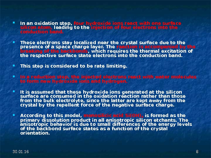
30. 01. 16 88 In an oxidation step, four hydroxide ions react with one surface silicon atom, leading to the injection of four electrons into the conduction band. These electrons stay localized near the crystal surface due to the presence of a space charge layer. The reaction is accompanied by the breaking of the backbonds , which requires thermal excitation of the respective surface state electrons into the conduction band. This step is considered to be rate limiting. In a reduction step, the injected electrons react with water molecules to form new hydroxide ions and hydrogen. It is assumed that these hydroxide ions generated at the silicon surface are consumed in the oxidation reaction rather than those from the bulk electrolyte, since the latter are kept away from the crystal by the repellent force of the negative surface charge. According to this model, monosilicic acid Si(OH) 4 is formed as the primary dissolution product in all anisotropic silicon etchants. The anisotropic behavior is due to small differences of the energy levels of the backbond surface states as a function of the crystal orientation.
30. 01. 16 99 Etch rate of Si in KOH Depends on Crystallographic Plane
30. 01. 16 1010 Etch rate of Si in KOH Depends on Temperature
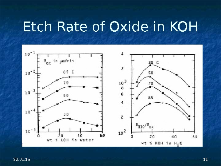
30. 01. 16 1111 Etch Rate of Oxide in KOH
30. 01. 16 1212 The etch rate of KOH and other alkaline etchants also slows greatly for heavily doped p-type (p ++++ ) silicon due to the lower concentration of electrons needed for this etch reaction to proceed. PP ++++ silicon is thus commonly used as an etch stop. The etch rate of undoped or n-type silicon in KOH solutions is approximately 0. 5 to 4 µm/min depending on the temperature and the concentration of KOH, but it drops by a factor of over 500 in p ++++ silicon with a dopant concentration above 1 × 10 2020 cmcm − 3− 3. . LPCVD Si 33 NN 44 is an excellent masking material against etching in KOH. Silicon dioxide etches at about 10 nm/min and can be used as a masking layer for very short etches. Photoresist is rapidly etched in hot alkaline solutions and is there-fore not suitable for masking these etchants.
30. 01. 16 1313 Anisotropic Etching of Crystalline Silicon in Alkaline Solutions II. Influence of Dopants J. Electrochem. Soc. , Vol. 137, No. 11, November 1990, pp. 3626 -3632 ABSTRACT The etching behavior of highly boron doped silicon in aqueous solutions based of ethylenediamine, KOH, Na. OH, a n d Li. OH was studied. For all etchants, a strong reduction of the etch rate for boron concentrations exceeding approximately 2 10 10 1919 cm cm -3 -3 was observed. This value is in good agreement with published data for the onset of degeneracy of p-type silicon. The reduction of the etch rate was found to be inversely proportional to the fourth power of the boron concentration. For a given high boron concentration, the etch stop effect was found to be most effective for ethylenediamine-based solutions and low concentration KOH and least effective for highly concentrated KOH.
30. 01. 16 1414 On the basis of these results, a model is proposed attributing the etch stop phenomenon to electrical effects of holes rather than chemical effects of boron. Due to the high dopant concentration the width of the space charge layer on the silicon surface shrinks drastically. Therefore, electrons injected into the conduction band by an oxidation reaction cannot be confined to the surface and rapidly recombine with holes from the valence band. The lack of these electrons impedes the reduction of water and thereby the formation of new hydroxide ions at the silicon surface. Since the transfer of four electrons is required for the dissolution of o n e silicon atom the observed fourth power law for the decrease of the etch rate can be explained. The reduction of the etch rate on silicon doped with germanium or phosphorus is much smaller and follows a different mechanism.
30. 01.
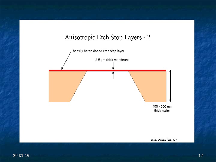
30. 01. 16 1616 Anisotropic Etch Stop Layers — 1 Controlling the absolute depth of an etch is often difficult, particularly if the etch is going most of the way through a wafer. Etch stop layers can be used to drastically slow the etch rate, providing a stopping point of high absolute accuracy. Boron doping is most commonly used for silicon etching. Requirements for specific etches: – HNA etch actually speeds up for heavier doping – KOH etch rate reduces by 20. for boron doping > 10 20 cm-3 – Na. OH etch rate reduces by 10. for boron doping > 3. 10 20 cm-3 – EDP etch rate reduces by 50. for boron doping > 7. 10 19 cm-3 – TMAH etch rate reduces by 10. for boron doping > 10 20 cm-
30. 01.
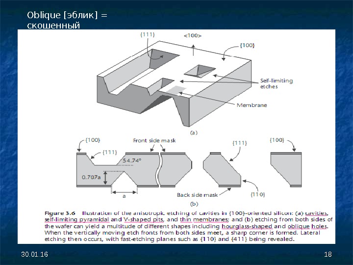
30. 01. 16 1818 Oblique [ эблик ] = скошенный
30. 01. 16 1919 Alkali hydroxides are extremely corrosive; aluminum bond pads inadvertently exposed to KOH are quickly damaged. CMOS fabrication facilities are very reluctant (сопротивляются) to use such etchants or even accept wafers that had previously been exposed to alkali hydroxides for fear (из-за боязни) of of contamination of potassium or sodium, two ions detrimental (пагубны) to the operation of MOS transistors.
30. 01. 16 2020 In the category of ammonium hydroxides, tetramethyl ammonium hydroxide (TMAH, N(CH 33 )) 44 OH) exhibits similar properties to KOH. It etches {111} crystallographic planes 30 to 50 times slower than {100} planes. The etch rate drops by a factor of 40 in heavily p-doped silicon (~1 × 10 2020 cmcm − 3− 3 ). A disadvantage of TMAH is the occasional formation of undesirable pyramidal hillocks at the bottom of the etched cavity.
30. 01. 16 2121 Both silicon dioxide and silicon nitride remain virtually unetched in TMAH and hence can be used as masking layers. It is advisable to remove native silicon dioxide in hydrofluoric acid prior to etching in TMAH because a layer just a few nanometers thick is sufficient to protect the silicon surface from etching. (Нужно удалять естественный окисел перед травлением в TMAH , т. к. даже он защищает Si Si от травления). TMAH normally attacks aluminum , but a special formulation containing silicon powder or a p. H-controlling additive dissolved in the solution significantly reduces the etch rate of aluminum. This property is useful for the etching of silicon after the complete fabrication of CMOS circuits without resorting (без выполнения) to the masking of the aluminum bond pads.
30. 01. 16 2222 EDP is another wet etchant with selectivity to {111} planes and to heavily p-doped silicon. It is is hazardous and its vapors are carcinogenic, necessitating the use of completely enclosed reflux condensers. Silicon oxides and nitrides are suitable masking materials for EDP etching. Many metals, including gold, chromium, copper, and tantalum, are also not attacked in EDP; however, the etch rate for aluminum is at about 0. 3 µm/min for the formulation given in Table 3. 2.
30. 01. 16 2323 Etching using anisotropic aqueous solutions results in three-dimensional faceted structures formed by intersecting {111} planes with other crystallographic planes. The design of the masking pattern demands a visualization in three dimensions of the etch procession. To that end, etch computer simulation software, such as the program ACES™ available from the University of Illinois at Urbana-Champaign, are useful design tools.
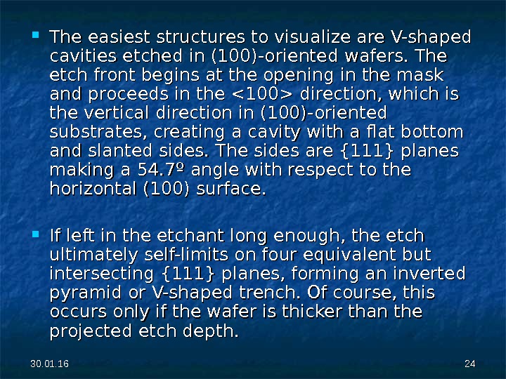
30. 01. 16 2424 The easiest structures to visualize are V-shaped cavities etched in (100)-oriented wafers. The etch front begins at the opening in the mask and proceeds in the direction, which is the vertical direction in (100)-oriented substrates, creating a cavity with a flat bottom and slanted sides. The sides are {111} planes making a 54. 7º angle with respect to the horizontal (100) surface. If left in the etchant long enough, the etch ultimately self-limits on four equivalent but intersecting {111} planes, forming an inverted pyramid or V-shaped trench. Of course, this occurs only if the wafer is thicker than the projected etch depth.
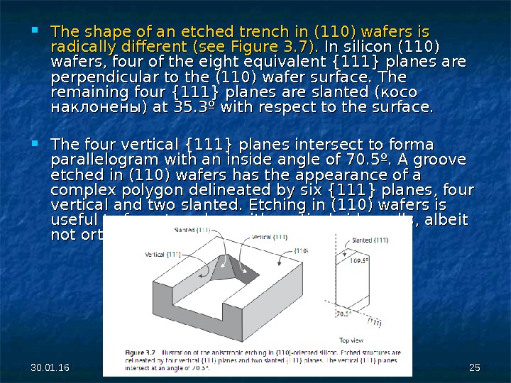
30. 01. 16 2525 The shape of an etched trench in (110) wafers is radically different (see Figure 3. 7). In silicon (110) wafers, four of the eight equivalent {111} planes are perpendicular to the (110) wafer surface. The remaining four {111} planes are slanted (( косо наклонены) at 35. 3º with respect to the surface. The four vertical {111} planes intersect to forma parallelogram with an inside angle of 70. 5º. A groove etched in (110) wafers has the appearance of a complex polygon delineated by six {111} planes, four vertical and two slanted. Etching in (110) wafers is useful to form trenches with vertical side-walls, albeit not orthogonal to each other.
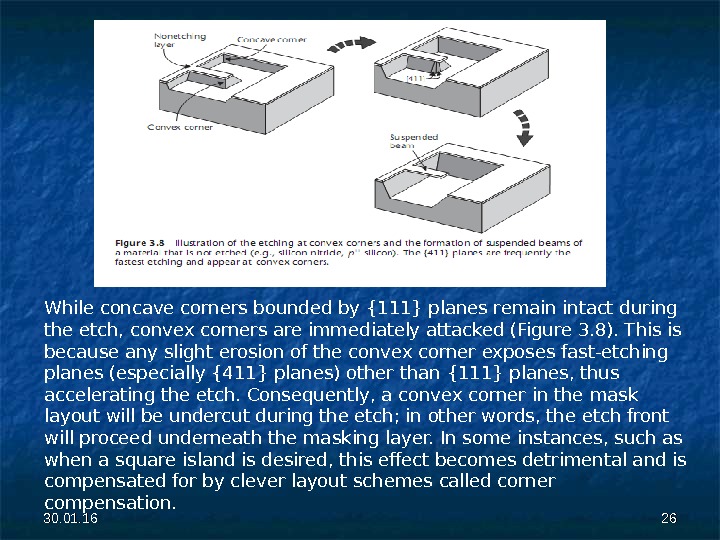
30. 01. 16 2626 While concave corners bounded by {111} planes remain intact during the etch, convex corners are immediately attacked (Figure 3. 8). This is because any slight erosion of the convex corner exposes fast-etching planes (especially {411} planes) other than {111} planes, thus accelerating the etch. Consequently, a convex corner in the mask layout will be undercut during the etch; in other words, the etch front will proceed underneath the masking layer. In some instances, such as when a square island is desired, this effect becomes detrimental and is compensated for by clever layout schemes called corner compensation.
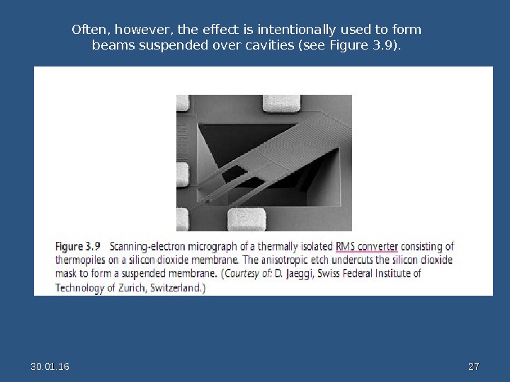
30. 01. 16 2727 Often, however, the effect is intentionally used to form beams suspended over cavities (see Figure 3. 9).
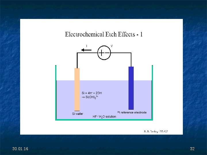
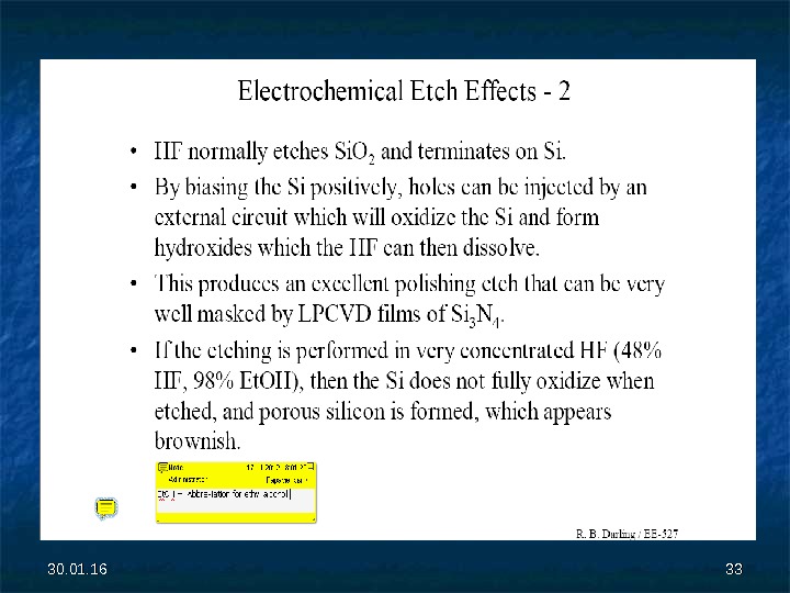
30. 01. 16 2828 Electrochemical Etching (ECE) The relatively large etch rates of anisotropic wet etchants (>0. 5 µm/min) make it difficult to achieve uniform and controlled etch depths. Some applications, such as bulk-micromachined pressure sensors, demand a thin (5 — to 20 -µm) silicon membrane with dimensional thickness control and uniformity of better than 0. 2 µm, which is very difficult to achieve using timed etching. Instead, the thickness control is obtained by using a precisely grown epitaxial layer and controlling the etch reaction with an externally applied electrical potential. This method is commonly referred as electrochemical etching (ECE). .
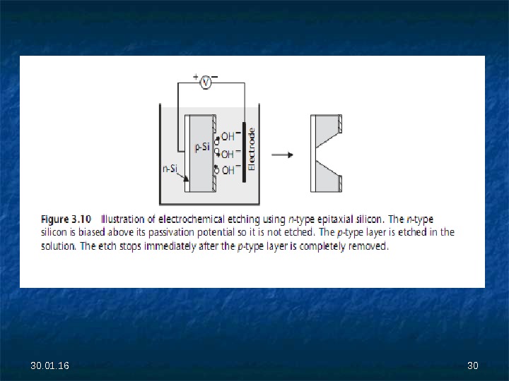
30. 01. 16 2929 • An n-type epitaxial layer grown on a p-type wafer forms a p-n junction diode that allows electrical conduction only if the p-type side is at a voltage above the n-type; otherwise, no electrical current passes and the diode is said to be in reverse bias. • During ECE, the applied potential is such that the p-n diode is in reverse bias, and the n-type epitaxial layer is above its passivation potential—the potential at which a thin passivating silicon dioxide layer forms—hence, it is not etched (see Figure 3. 10). • The p-type substrate is allowed to electrically float, so it is etched. • As soon as the p-type substrate is completely removed, the etch reaction comes to a halt at the junction, leaving a layer of n-type silicon with precise thickness.
30. 01.
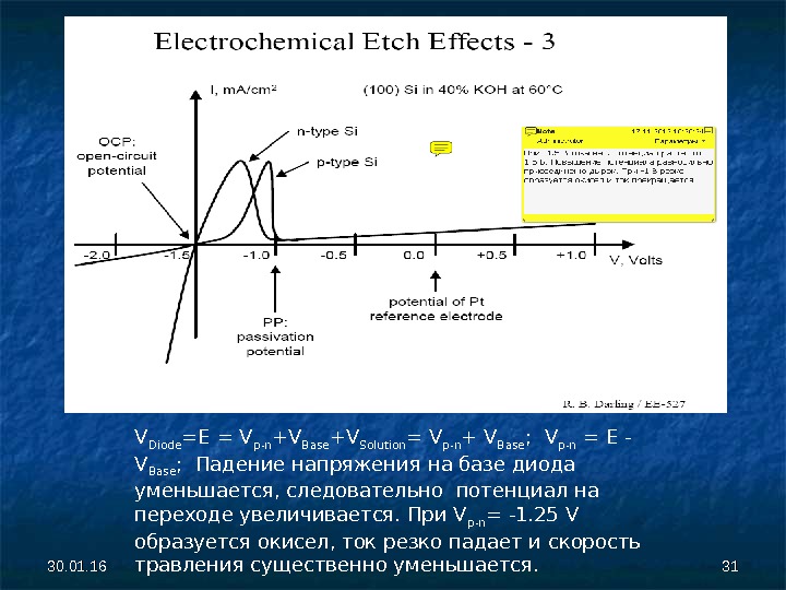
30. 01. 16 3131 V Diode = E = V p — n + V B ase + V Solution = V p -n + V B ase ; V p — n = E — V B ase ; Падение напряжения на базе диода уменьшается, следовательно потенциал на переходе увеличивается. При V p — n = -1. 25 V образуется окисел, ток резко падает и скорость травления существенно уменьшается.
30. 01.
30. 01.
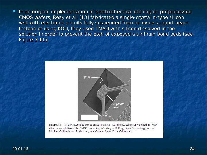
30. 01. 16 3434 In an original implementation of electrochemical etching on preprocessed CMOS wafers, Reay et al. [13] fabricated a single-crystal n-type silicon well with electronic circuits fully suspended from an oxide support beam. Instead of using KOH, they used TMAH with silicon dissolved in the solution in order to prevent the etch of exposed aluminum bond pads (see Figure 3. 11).