
30. 01. 16 11 Deposition of Silicon Nitrides


processes_for_micromachining-lecture_2.ppt
- Размер: 1.9 Mегабайта
- Количество слайдов: 44
Описание презентации 30. 01. 16 11 Deposition of Silicon Nitrides по слайдам
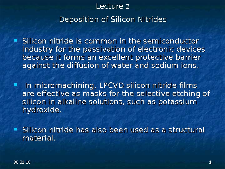
30. 01. 16 11 Deposition of Silicon Nitrides Silicon nitride is common in the semiconductor industry for the passivation of electronic devices because it forms an excellent protective barrier against the diffusion of water and sodium ions. In micromachining, LPCVD silicon nitride films are effective as masks for the selective etching of silicon in alkaline solutions, such as potassium hydroxide. Silicon nitride has also been used as a structural material. Lecture
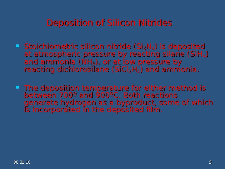
30. 01. 16 22 Deposition of Silicon Nitrides Stoichiometric silicon nitride (Si 33 NN 44 ) is deposited at atmospheric pressure by reacting silane (Si. H 44 ) ) and ammonia (NH 33 ), or at low pressure by reacting dichlorosilane (Si. Cl 22 HH 22 ) and ammonia. The deposition temperature for either method is between 700º and 900ºC. Both reactions generate hydrogen as a byproduct, some of which is incorporated in the deposited film.
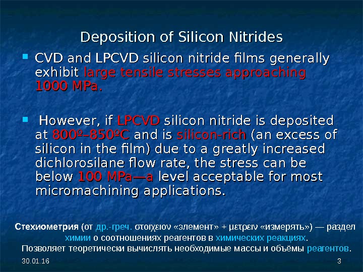
30. 01. 16 33 Deposition of Silicon Nitrides CVD and LPCVD silicon nitride films generally exhibit large tensile stresses approaching 1000 MPa. However, if LPCVD silicon nitride is deposited at at 800º– 850ºC and is silicon-rich (an excess of silicon in the film) due to a greatly increased dichlorosilane flow rate, the stress can be below 100 MPa—a level acceptable for most micromachining applications. Стехиометрия (от др. -греч. στοιχειον «элемент» +μετρειν «измерять» )—раздел химии осоотношенияхреагентовв химическихреакциях. Позволяеттеоретическивычислятьнеобходимыемассыиобъёмы реагентов.
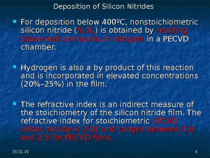
30. 01. 16 44 Deposition of Silicon Nitrides For deposition below 400ºC, nonstoichiometric silicon nitride ( Si. Sixx NNyy ) is obtained by reacting silane with ammonia or nitrogen in a PECVD chamber. Hydrogen is also a by product of this reaction and is incorporated in elevated concentrations (20%– 25%) in the film. The refractive index is an indirect measure of the stoichiometry of the silicon nitride film. The refractive index for stoichiometric LPCVD silicon nitride is 2. 01 and ranges between 1. 8 and 2. 5 for PECVD films.
30. 01. 16 55 Deposition of Silicon Nitrides A high value in the range is indicative of excess silicon, and a low value generally represents an excess of nitrogen. . One of the key advantages of PECVD nitride is the ability to control stress during deposition. Silicon nitride deposited at a plasma excitation frequency of 13. 56 MHz exhibits tensile stress of of about 400 MPa , whereas a film deposited at a frequency of 50 k. Hz has a compressive stress of 200 MPa. By alternating frequencies during deposition, one may obtain lower-stress films.
30. 01. 16 66 Spin-On Methods Spin-on is a process to put down layers of dielectric insulators and organic materials. The equipment is simple, requiring a variable-speed spinning table with appropriate safety screens. A nozzle dispenses the material as a liquid solution in the center of the wafer. Spinning the substrate at speeds of 500 to 5000 rpm for 30 to 60 seconds spreads the material to a uniform thickness.
30. 01. 16 77 Photoresists and polyimides are common organic materials that can be spun on a wafer with thicknesses typically between 0. 5 and 20 µmµm , though some special-purpose resists such as epoxy-based SU-8 can exceed 200 µm. . The organic polymer is normally in suspension in a solvent solution; subsequent baking causes the solvent to evaporate, forming a firm film. Spin-On Methods
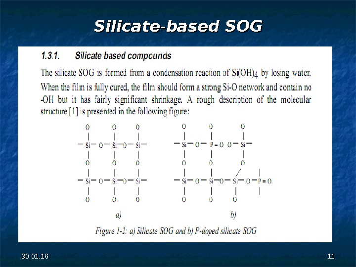
30. 01. 16 88 Spin-On Methods Thick (5– 100 µm) spin-on glass (SOG) has the ability to uniformly coat surfaces and smooth out underlying topographical variations, effectively planarizing surface features. Thin (0. 1– 0. 5 µm) SOG was heavily investigated in the integrated circuit industry as an interlayer dielectric between metals for high-speed electrical interconnects; however, its electrical properties are considered poor compared to thermal or CVD silicon oxides. Spin-on glass is commercially available in different forms, commonly siloxane- or silicate-based. . The latter type allows water absorption into the film, resulting in a higher relative dielectric constant and a tendency to crack. After deposition, the layer is typically densified at a temperature between 300º and 500ºC. . Measured film stress is approximately 200 MPa in tension but decreases substantially with increasing anneal temperatures.
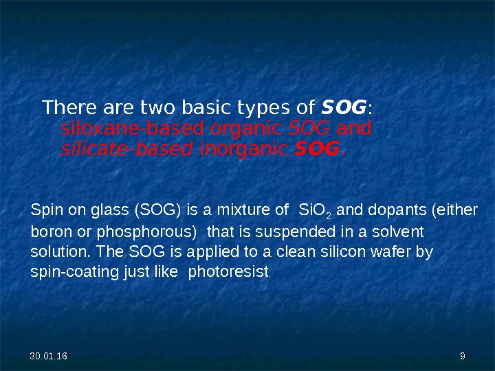
30. 01. 16 99 There are two basic types of SOG : siloxane-based organic SOG and silicate — based inorganic SOG. Spinonglass(SOG)isamixtureof. Si. O 2 anddopants(either boronorphosphorous) that issuspendedinasolvent solution. The. SOGisappliedtoacleansiliconwaferby spin-coatingjustlikephotoresist.
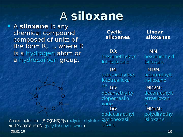
30. 01. 16 1010 A A siloxanesiloxane is any chemical compound composed of units of the form R 22 Si. Si OO , where R is a hydrogen atom or a a hydrocarbon group. Cyclic siloxanes Linear siloxanes D 3: hexamethylcyc lotrisiloxane MM: hexamethyld isiloxane D 4: octamethylcyc lotetrasiloxa nene MDM: octamethylt risiloxane D 5: decamethylcy clopentasilo xane MD 2 M: decamethylt etrasiloxan ee D 6: dodecamethyl cyclohexasil oxane MDn. M: polydimethy lsiloxane Ane xamplesare : [Si. O(CH 3)2] n ( polydimethylsiloxane ) and[Si. O(C 6 H 5)2] n ( polydiphenylsiloxane ).
30. 01. 16 1111 SS ilicate — based SOG
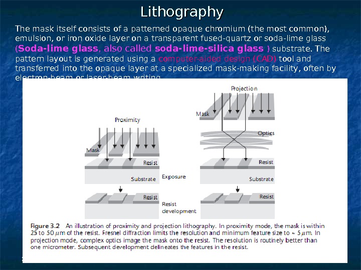
30. 01. 16 1212 Lithography The mask itself consists of a patterned opaque chromium (the most common), emulsion, or iron oxide layer on a transparent fused-quartz or soda-lime glass ( Soda-lime glass , also called soda-lime-silica glass ) substrate. The pattern layout is generated using a computer-aided design (CAD) tool and transferred into the opaque layer at a specialized mask-making facility, often by electron-beam or laser-beam writing.
30. 01. 16 1313 Soda-lime glass , also called soda-lime-silica glass , is the most prevalent type of glass , used for windowpanes, and glass containers (bottles and jars). Soda-lime glass is prepared by melting the raw materials , such as sodium carbonate (soda), lime , , dolomite , , silicon dioxide (silica), aluminium oxide (alumina), and small quantities of fining agents (e. g. , sodium sulfate , , sodium chloride ) in a glass furnace at at temperatures locally up to 1675 °C. Lime (известь) is a calcium -containing inorganic material in which carbonates , , oxides and hydroxides predominate. Strictly speaking, lime is calcium oxide or or calcium hydroxide. It is also the name of the natural mineral (native lime) Ca. O which occurs as a product of coal seam fires and in altered limestone xenoliths in in volcanic ejecta. The word «lime» originates with its earliest use as building mortar and has the sense of «sticking or adhering.
Soda-lime glass is divided technically into glass used for windows, called flat glass , and glass for containers, called container glass. The two types differ in the application, production method ( float process for windows, blowing and pressing for containers), and chemical composition. Float glass has a higher magnesium oxide andand sodium oxide content than container glass, and a lower silica, calcium oxide , and aluminium oxide content. From this follows the slightly higher quality of container glass for chemical durability against water, which is required especially for storage of beverages and food. 30. 01.
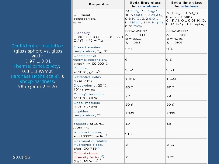
30. 01. 16 1515 Coefficient of restitution (glass sphere vs. glass wall): 0. 97 ± 0. 01 Thermal conductivity : 0. 9 -1. 3 W/m. K Hardness (Mohs scale) : 6 Knoop hardness : 585 kg/mm 2+
30. 01. 16 1616 Lime is a general term for calcium -containing inorganic materials, in which carbonates , , oxides andand hydroxides predominate. Strictly speaking, lime is calcium oxide oror calcium hydroxide. It is also the name of the natural mineral (native lime) of the Ca. O composition which occurs as a product ofof coal seam fires and in altered limestone xenoliths inin volcanic ejecta. The word «lime» originates with its earliest use as building mortar and has the sense of «sticking or adhering. » These materials are still used in large quantities as building and engineering materials (including limestone products, concrete andand mortar ) and as chemical feedstocks, among other uses. Lime industries and the use of many of the resulting products date from prehistoric periods in both the Old World and the. New World. Lime is used extensively forwaste water treatmentwithferrous sulfate. The rocks and minerals from which these materials are derived, typicallylimestoneorchalk, are composed primarily ofcalcium carbonate. They may be cut, crushed or pulverized and chemically altered. «Burning» (calcination) converts them into the highlycausticmaterial quicklime (calcium oxide, Ca. O) and, through subsequent addition of water, into the less caustic (but still stronglyalkaline) slaked lime oror hydrated lime (calcium hydroxide, Ca(OH) 22 ), the process of which is called slaking of lime. . When the term is encountered in an agricultural context, it probably refers toagricultural lime. Otherwise it most commonly meansslaked lime, as the more dangerous form is usually described more specifically asquicklimeor burnt lime. .
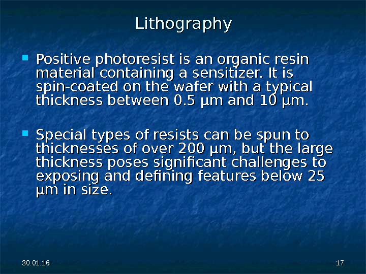
30. 01. 16 1717 Lithography Positive photoresist is an organic resin material containing a sensitizer. It is spin-coated on the wafer with a typical thickness between 0. 5 µm and 10 µm. Special types of resists can be spun to thicknesses of over 200 µm, but the large thickness poses significant challenges to exposing and defining features below 25 µm in size.
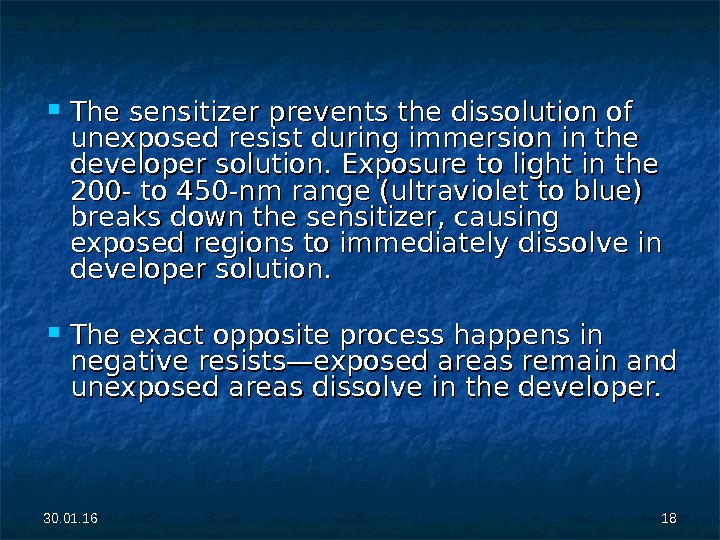
The sensitizer prevents the dissolution of unexposed resist during immersion in the developer solution. Exposure to light in the 200 — to 450 -nm range (ultraviolet to blue) breaks down the sensitizer, causing exposed regions to immediately dissolve in developer solution. The exact opposite process happens in negative resists—exposed areas remain and unexposed areas dissolve in the developer. 30. 01.
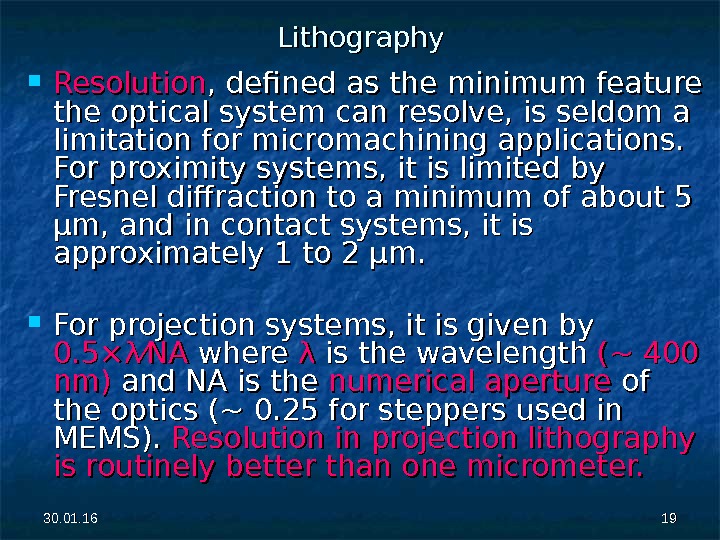
30. 01. 16 1919 Lithography Resolution , defined as the minimum feature the optical system can resolve, is seldom a limitation for micromachining applications. For proximity systems, it is limited by Fresnel diffraction to a minimum of about 5 µm, and in contact systems, it is approximately 1 to 2 µm. For projection systems, it is given by 0. 5×λ⁄NA where λλ is the wavelength (~ 400 nm)nm) and NA is the numerical aperture of of the optics (~ 0. 25 for steppers used in MEMS). Resolution in projection lithography is is routinely better than one micrometer.
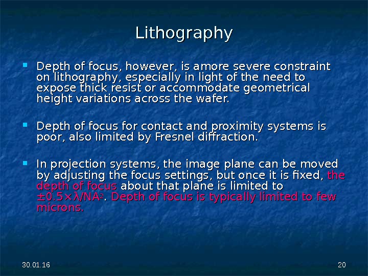
30. 01. 16 2020 Lithography Depth of focus, however, is amore severe constraint on lithography, especially in light of the need to expose thick resist or accommodate geometrical height variations across the wafer. Depth of focus for contact and proximity systems is poor, also limited by Fresnel diffraction. In projection systems, the image plane can be moved by adjusting the focus settings, but once it is fixed, the depth of focus about that plane is limited to ± 0. 5×λ/NA 22. . Depth of focus is typically limited to few microns.
30. 01. 16 2121 Projection lithography is clearly a superior approach, but an optical projection system can cost significantly more than a proximity or contact system. Long-term cost of ownership plays a critical role in the decision to acquire a particular lithographic tool. While resolution of most lithographic systems is not a limitation for MEMS, lithography can be challenging depending on the nature of the application; examples include exposure of thick resist , , topographical height variations , , front to back side pattern alignment , , and large fields of view. Lithography
30. 01. 16 2222 Thick Resist Patterned thick resist is normally used as a protective masking layer for the etching of deep structures and can also be used as a template for the electroplating of metal microstructures. Coating substrates with thick resist is achieved either by multiple spin-coating applications (up to a total of 20 µm) or by spinning special viscous resist solutions at slower speeds (up to 100 µm). Maintaining thickness control and uniformity across the wafer becomes difficult with increasing resist thickness.
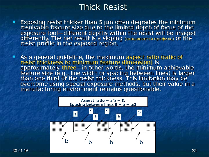
30. 01. 16 2323 Thick Resist Exposing resist thicker than 5 µm often degrades the minimum resolvable feature size due to the limited depth of focus of the exposure tool—different depths within the resist will be imaged differently. The net result is a sloping (скашивается профиль) of the resist profile in the exposed region. As a general guideline, the maximum aspect ratio (ratio of resist thickness to minimum feature dimension) is is approximately three —in other words, the minimum achievable feature size (e. g. , line width or spacing between lines) is larger than one third of the resist thickness. This limitation may be overcome using special exposure methods, but their value in a manufacturing environment remains questionable. b SAspect ratio = a/b = 3. Spacing between lines S = b = a/3 b ba a a a. S SS b b
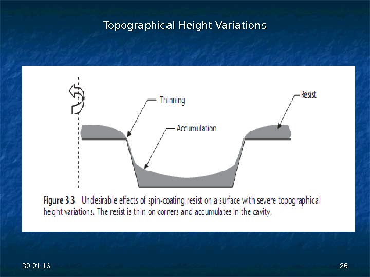
30. 01. 16 2424 Topographical Height Variations Changes in topography on the surface of the wafer, such as deep cavities and trenches, are common in MEMS and pose challenges (вызывает проблемы) to both resist spinning and imaging. For cavities deeper than about 10 µm , thinning of the resist at convex corners and accumulation inside the cavity create problems with exposure and with leaving insufficient resist thickness during etches (see Figure 3. 3). Two recent developments targeting resist coating of severe topography are spray-on resist and electroplated resist.
30. 01. 16 2525 Topographical Height Variations Exposing a pattern on a surface with height variations in excess of 10 µm is also a difficult task because of the limited depth of focus. . Contact and proximity tools are not suitable for this task unless a significant loss of resolution is tolerable. Under certain circumstances where the number of height levels is limited (say, less than three), one may use a projection lithography tool to perform an exposure with a corresponding focus adjustment at each of these height levels. Naturally, this is costly because the number of masks and exposures increases linearly with the number of height levels.
30. 01. 16 2626 Topographical Height Variations
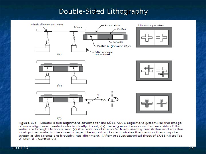
30. 01. 16 2727 Double-Sided Lithography Often, lithographic patterns on both sides of a wafer need to be aligned with respect to each other with high accuracy. For example, the fabrication of a commercial pressure sensor entails forming on the front side of the wafer piezoresistive sense elements that are aligned to the edges of a cavity on the back side of the wafer. Different methods of front-to-back side alignment, also known as double-sided alignment, have been incorporated in commercially available tools. Wafers polished on both sides should be used to minimize light scattering during lithography.
30. 01. 16 2828 Double-Sided Lithography
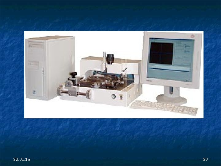
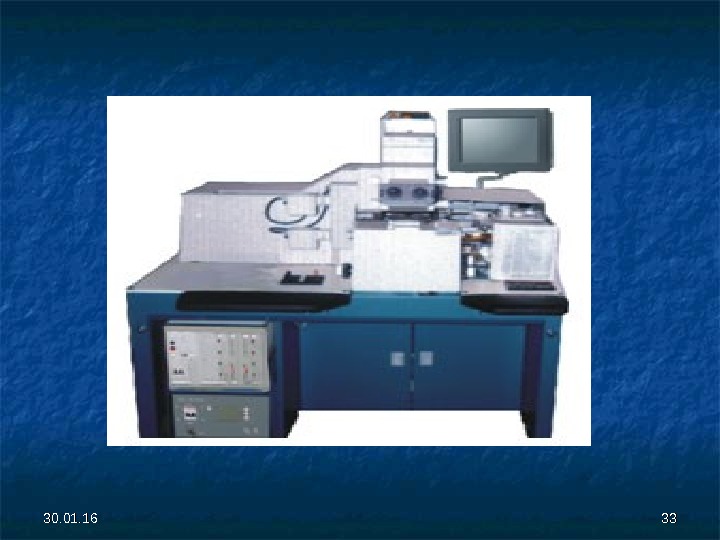
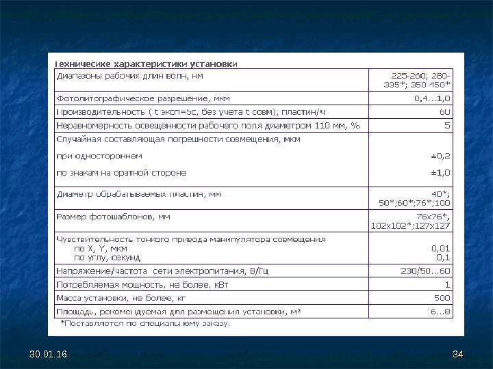
30. 01. 16 2929 ЭМ-5086 УСТАНОВКА ДВУСТОРОННЕГО СОВМЕЩЕНИЯ И ЭКСПОНИРОВАНИЯ ЗНАКОВ СОВМЕЩЕНИЯ Установка предназначена для нанесения знаков совмещения наобратную сторону пластины, совмещенных со знаками совмещения, сформированными предварительно на еёлицевой стороне. Работа установки основана на проекционном переносе изображения знака совмещения наобратную сторону пластины. Знаки совмещения на нижней стороне пластины формируются точно напротив знаков совмещения налицевой стороне пластины. Установка применяется в фотолитографических процессах при изготовлении полупроводниковых, гибридных, оптических, оптоэлектронных, МЭМС, МОЭМС и других приборов. Применение этой установки позволяет использовать оборудование для односторонней контактной или проекционной фотолитографии для двустороннего технологического процесса вместо использования установок для двусторонней фотолитографии.
30. 01.
30. 01.
30. 01. 16 3232 ЭМ-5026 Б УСТАНОВКА ДВУСТОРОННЕГО СОВМЕЩЕНИЯ И ЭКСПОНИРОВАНИЯ Установка ЭМ– 5026 Б выполняет контактным (в зазоре) способом экспонирование верхней стороны полупроводниковой пластины или подложки, совмещая изображение на фотошаблоне с изображением наобратной стороне пластины или подложки. При этом дополнительно возможна оценка точностисовмещения знаков и изображений (топологий) на двух сторонах пластины(подложки).
30. 01.
30. 01.
30. 01. 16 3535 Large Field of View (Большая область экспонирования) The field of view is the extent of the area that is exposed at any one time on the wafer. Область проецирования это область, которая экспонируется в любой момент на пластину. In proximity and contact lithography, it covers the entire wafer. В проекционной и контактной литографии эта область покрывает всю пластину.
30. 01. 16 3636 In projection systems, the field of view is often less than 1 × 1 cm 22. . The entire wafer is exposed by stepping the small field of view across in a two-dimensional array, hence the stepper appellation. В проекционной литографии эта область часто меньше чем 1 × 1 cm 22. Поэтому вся пластина экспонируется пошагово малыми фрагментами, как двумерный массив. In some applications, the device structure may span dimensions exceeding the field of view. A remedy to this is called field stitching, inin which two or more different fields are exposed sequentially, with the edges of the fields overlapping. В некоторых приборах структура может иметь размеры, превышающие область экспонирования. Для решения этой проблемы делают области сшивания, которые находятся по краям сопрягаемых областей. Large Field of View (Большая область экспонирования)
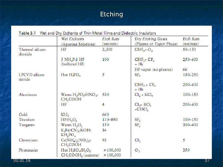
30. 01. 16 3737 Etching
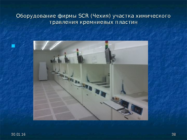
30. 01. 16 3838 Оборудование фирмы SCR (Чехия) участка химического травления кремниевых пластин
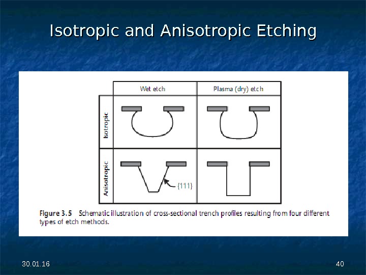
30. 01. 16 3939 Isotropic Wet Etching The most common group of silicon isotropic wet etchants is HNA, also known as isoiso etch and poly etch because of its use in the early days of the integrated circuit industry as an etchant for polysilicon. It is a mixture of hydrofluoric (HF), nitric (HNO 33 ), and acetic (CH(CH 33 COOH) acids, although water may replace the acetic acid. In the chemical reaction, the nitric acid oxidizes silicon, which is then etched by the hydrofluoric acid. The etch rate of silicon can vary from 0. 1 to over 100 µm/min depending on the proportion of the acids in the mixture. Etch uniformity is normally difficult to control but is improved by stirring.
30. 01. 16 4040 Isotropic and Anisotropic Etching
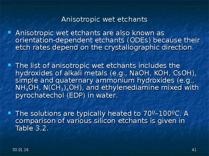
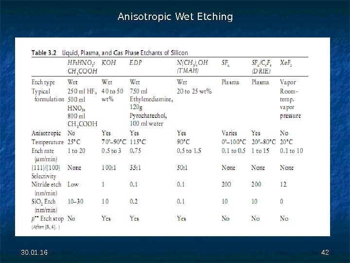
30. 01. 16 4141 Anisotropic wet etchants are also known as orientation-dependent etchants (ODEs) because their etch rates depend on the crystallographic direction. The list of anisotropic wet etchants includes the hydroxides of alkali metals (e. g. , Na. OH, KOH, Cs. OH), simple and quaternary ammonium hydroxides (e. g. , NHNH 44 OH, N(CH 33 )) 44 OH), and ethylenediamine mixed with pyrochatechol (EDP) in water. . The solutions are typically heated to 70º– 100ºC. A comparison of various silicon etchants is given in Table 3. 2.
30. 01. 16 4242 Anisotropic Wet Etching
30. 01. 16 4343 KOH is by far the most common ODE Etch rates are typically given in the [100] direction, corresponding to the etch front being the (100) plane. The {110} planes are etched in KOH about twice as rapidly as {100} planes. While {111} planes are etched at a rate about 100 times slower than for {100} planes.
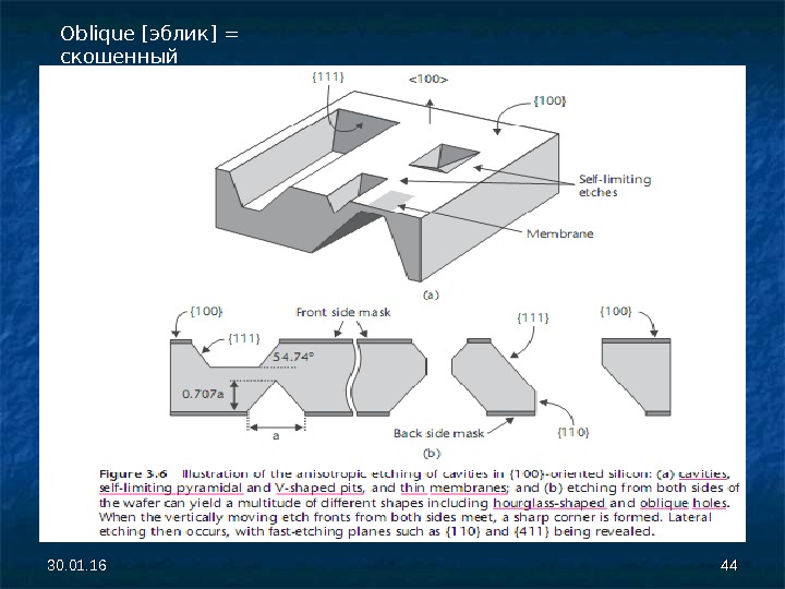
30. 01. 16 4444 Oblique [ эблик ] = скошенный