a856c0d3e50f6a0ff08582d3589bcaaa.ppt
- Количество слайдов: 194
 15 CS 205 J/MICROPROCESSORS AND MICROCONTROLLERS UNIT - 1 Introduction to Microprocessor and Family 1
 Introduction –Microprocessors and Microcontrollers-its computational functionality and importance -8086 architecture and historical background-The Microprocessor based personal computer Systems-Internal Microprocessor architecture-Real mode memory addressing-Protected mode Memory Addressing. 2
 3
3
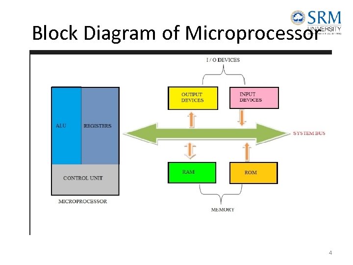 Block Diagram of Microprocessor 4
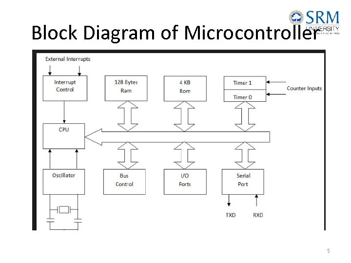 Block Diagram of Microcontroller 5
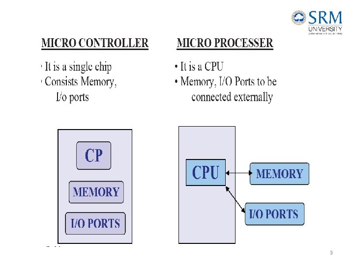
 Microprocessor: A silicon chip that contains a CPU. The terms microprocessor and CPU are used interchangeably. A microprocessor (abbreviated μP) is a digital electronic component with miniaturized transistors on a single semiconductor integrated circuit (IC). 6
 • To access the local descriptor table, the LDTR (local descriptor table register) is loaded with a selector. – selector accesses global descriptor table, & loads local descriptor table address, limit, & access rights into the cache portion of the LDTR • The TR (task register) holds a selector, which accesses a descriptor that defines a task. – a task is most often a procedure or application • Allows multitasking systems to switch tasks to another in a simple and orderly fashion. 7
 Three basic characteristics differentiate microprocessors: • Instruction set: The set of instructions that the microprocessor can execute. • Bandwidth: The number of bits processed in a single instruction. • Clock speed: Given in megahertz (MHz), the clock speed determines how many instructions per second the processor can execute. 8
 9
9
 Microcontroller: Integrated electronic computing device that includes three major components on a single chip • Microprocessor (MPU)/Central Processing Unit (CPU) • Memory • I/O (Input/Output) ports • A microcontroller differs from a microprocessor, which is a general-purpose chip that is used to create a multi-function computer or device and requires multiple chips to handle various tasks. 10
 Microcontrollers • Support Devices – Timers – A/D converter – Serial I/O • Common communication lines – System Bus • Microcontroller is designed for a very specific task - to control a particular system. 11
 Features of Intel 8086 Microprocessor: 1. Intel 8086 was launched in 1978. 2. It was the first 16 -bit microprocessor. 3. This microprocessor had major improvement over the execution speed of 8085. 4. It is available as 40 -pin Dual-Inline-Package (DIP). 5. The 8086 is able to address 1 MB of physical memory. 12
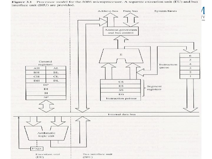
 1. Intel 8086 Architecture • The 8086 CPU is divided into two independent functional units: • 1. Bus Interface Unit (BIU) • 2. Execution Unit (EU) 13
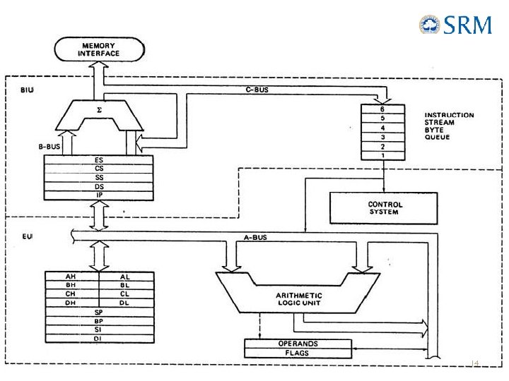 8086 Architecture 14
 Bus Interface Unit (BIU) The function of BIU is to: • Fetch the instruction or data from memory. • Write the data to the port. • Read data from the port. 15
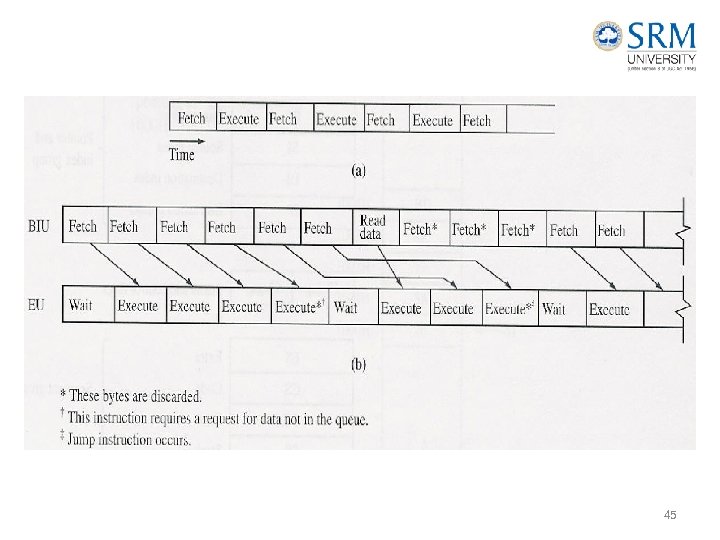
 Instruction Queue 1. To increase the execution speed, BIU fetches as many as six instruction bytes ahead to time from memory. 2. All six bytes are then held in first out 6 byte register called instruction queue. 3. Then all bytes have to be given to EU one by one. 4. This pre fetching operation of BIU may be in parallel with execution operation of EU, which improves the speed execution of the instruction. 16
 Execution Unit (EU) • The functions of execution unit are: • To tell BIU where to fetch the instructions or data from. • To decode the instructions. • To execute the instructions. 17
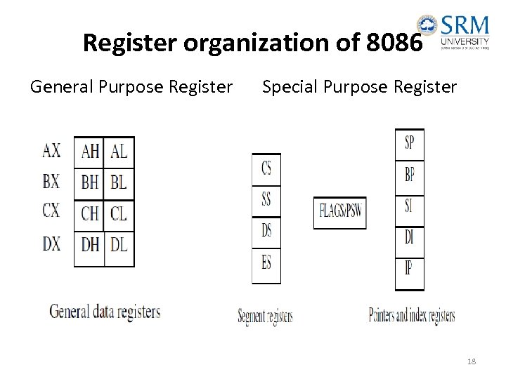 Register organization of 8086 General Purpose Register Special Purpose Register 18
 General Purpose Registers of 8086 • These registers can be used as 8 -bit registers individually or can be used as 16 -bit in pair to have AX, BX, CX, and DX. 1. AX Register: AX register is also known as accumulator register that stores operands for arithmetic operation like divided, rotate. 2. BX Register: This register is mainly used as a base register. It holds the starting base location of a memory region within a data segment. 3. CX Register: It is defined as a counter. It is primarily used in loop instruction to store loop counter. 4. DX Register: DX register is used to contain I/O port address for I/O instruction. 19
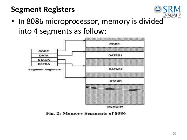 Segment Registers • In 8086 microprocessor, memory is divided into 4 segments as follow: 20
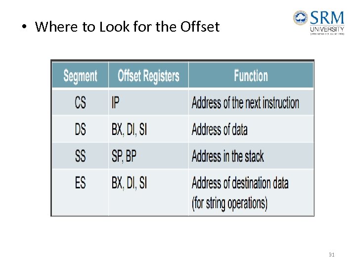
 • 1. Code Segment (CS): The CS register is used for addressing a memory location in the Code Segment of the memory, where the executable program is stored. • 2. Data Segment (DS): The DS contains most data used by program. Data are accessed in the Data Segment by an offset address or the content of other register that holds the offset address. • 3. Stack Segment (SS): SS defined the area of memory used for the stack 21
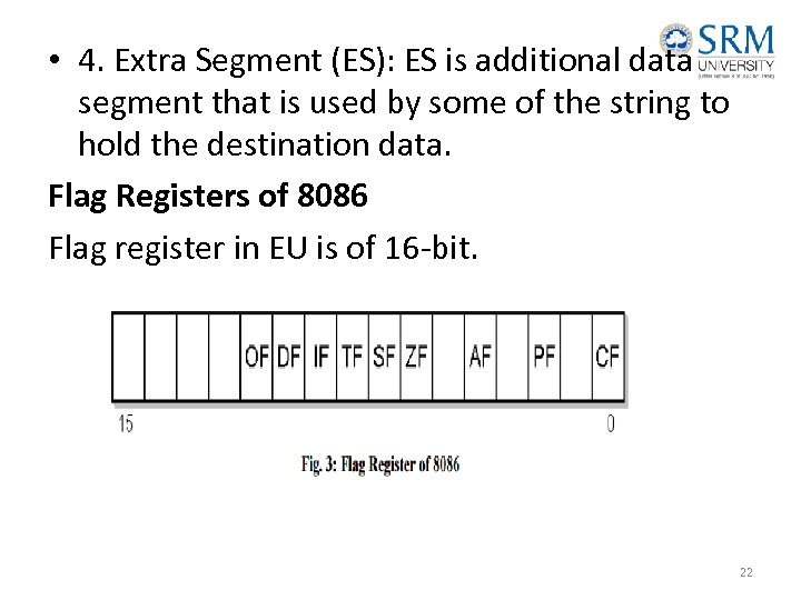 • 4. Extra Segment (ES): ES is additional data segment that is used by some of the string to hold the destination data. Flag Registers of 8086 Flag register in EU is of 16 -bit. 22
 • Flags Register determines the current state of the processor. • They are modified automatically by CPU after mathematical operations, this allows to determine the type of the result, and to determine conditions to transfer control to other parts of the program. • 8086 has 9 flags and they are divided into two categories: • 1. Conditional Flags 2. Control Flags 23
 Conditional Flags Conditional flags represent result of last arithmetic or logical instruction executed. Conditional flags are as follows: 1. Carry Flag (CF): Indicates an overflow condition for unsigned integer arithmetic. 2. Auxiliary Flag (AF): If an operation performed in ALU generates a carry/barrow from lower nibble (i. e. D 0 – D 3) to upper nibble (i. e. D 4 – D 7), the AF flag is set i. e. carry given by D 3 bit to D 4 is AF flag. 3. Parity Flag (PF): This flag is used to indicate the parity of result. If lower order 8 -bits of the result contains even number of 1’s, the Parity Flag is set and for odd number of 1’s, the Parity Flag is reset. 24
 4. Zero Flag (ZF): It is set; if the result of arithmetic or logical operation is zero else it is reset. 5. Sign Flag (SF): In sign magnitude format the sign of number is indicated by MSB bit. If the result of operation is negative, sign flag is set. 6. Overflow Flag (OF): It occurs when signed numbers are added or subtracted. An OF indicates that the result has exceeded the capacity of machine. 25
 Control Flags • Control flags are set or reset deliberately to control the operations of the execution unit. Control flags are as follows: 1. Trap Flag (TP): A trap flag permits operation of a processor in single-step mode. 2. Interrupt Flag (IF): a. It is an interrupt enable/disable flag. b. If it is set, the maskable interrupt of 8086 is enabled and if it is reset, the interrupt is disabled. 26
 3. Direction Flag (DF): • a. It is used in string operation. • b. If it is set, string bytes are accessed from higher memory address to lower memory • address. • c. When it is reset, the string bytes are accessed from lower memory address to higher • memory address. 27
 Memory Segmentation Intel 8086 has 20 lines address bus. 2 power 20 = 1, 048, 576 bytes (1 MB). The total 1 MB of memory is divided into 16 segments of each of 64 KB. The address of the segments are 0000 H to F 000 H. The offset address values are from 0000 H to FFFFH. In 8086, memory has four different types of segments. 1. Code Segment 2. Data Segment 3. Stack Segment 4. Extra Segment 28
 • Each register stores the base address (starting address) of the corresponding segment. Because the segment registers cannot store 20 bits, they only store the upper 16 bits. • The 20 -bit address of a byte is called its Physical Address. But, it is specified as a Logical Address. Logical address is in the form of: Base Address : Offset • Offset is the displacement of the memory location from the starting location of the segment. 29
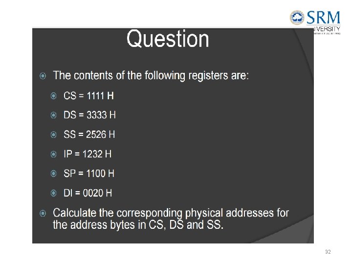
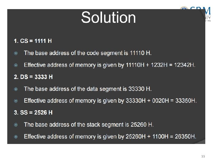
 • If the data at any location has a logical address specified as: 2222 H : 0016 H • Then, the number 0016 H is the offset. • 2222 H is the value of DS. • BIU MULTIPLIES DS WITH 10 H, THEN ADD THAT VALUE WITHOFFSET. • 10 H*DS =>22220 + • OFFSET => 0016 =>22236 =>EA/PA 30
 • Where to Look for the Offset 31
 32
32
 33
33
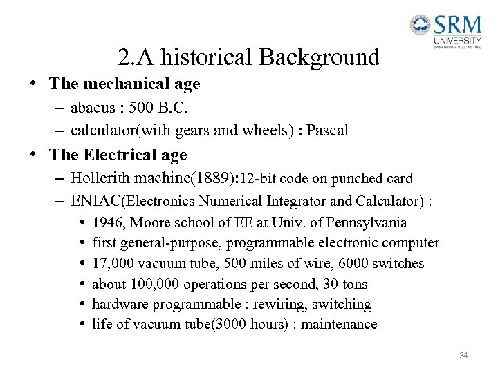 2. A historical Background • The mechanical age – abacus : 500 B. C. – calculator(with gears and wheels) : Pascal • The Electrical age – Hollerith machine(1889): 12 -bit code on punched card – ENIAC(Electronics Numerical Integrator and Calculator) : • • • 1946, Moore school of EE at Univ. of Pennsylvania first general-purpose, programmable electronic computer 17, 000 vacuum tube, 500 miles of wire, 6000 switches about 100, 000 operations per second, 30 tons hardware programmable : rewiring, switching life of vacuum tube(3000 hours) : maintenance 34
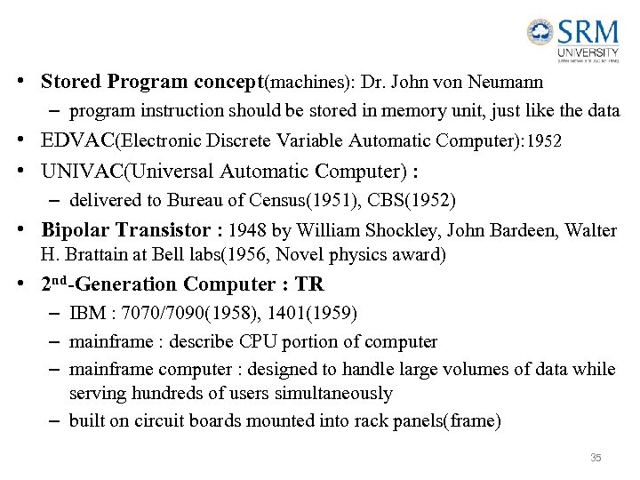 • Stored Program concept(machines): Dr. John von Neumann – program instruction should be stored in memory unit, just like the data • EDVAC(Electronic Discrete Variable Automatic Computer): 1952 • UNIVAC(Universal Automatic Computer) : – delivered to Bureau of Census(1951), CBS(1952) • Bipolar Transistor : 1948 by William Shockley, John Bardeen, Walter H. Brattain at Bell labs(1956, Novel physics award) • 2 nd-Generation Computer : TR – IBM : 7070/7090(1958), 1401(1959) – mainframe : describe CPU portion of computer – mainframe computer : designed to handle large volumes of data while serving hundreds of users simultaneously – built on circuit boards mounted into rack panels(frame) 35
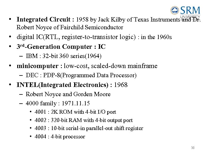 • Integrated Circuit : 1958 by Jack Kilby of Texas Instruments and Dr. Robert Noyce of Fairchild Semiconductor • digital IC(RTL, register-to-transistor logic) : in the 1960 s • 3 rd-Generation Computer : IC – IBM : 32 -bit 360 series(1964) • minicomputer : low-cost, scaled-down mainframe – DEC : PDP-8(Programmed Data Processor) • INTEL(Integrated Electronics) : 1968 – Robert Noyce and Gorden Moore – 4000 family : 1971. 15 • • 4001 : 2 K ROM with 4 -bit I/O port 4002 : 320 -bit RAM with 4 -bit output port 4003 : 10 -bit serial-in parallel-out shift register 4004 : 4 -bit processor 36
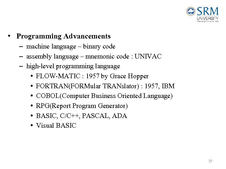 • Programming Advancements – machine language – binary code – assembly language – mnemonic code : UNIVAC – high-level programming language • FLOW-MATIC : 1957 by Grace Hopper • FORTRAN(FORMular TRANslator) : 1957, IBM • COBOL(Computer Business Oriented Language) • RPG(Report Program Generator) • BASIC, C/C++, PASCAL, ADA • Visual BASIC 37
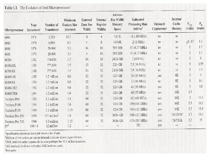
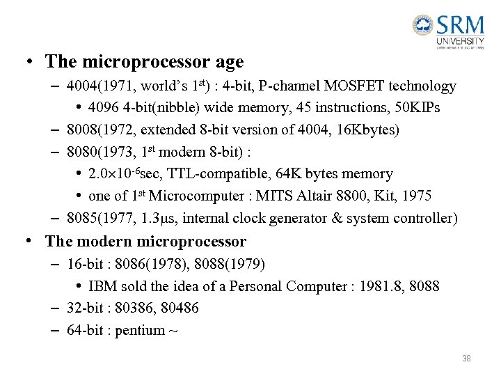 • The microprocessor age – 4004(1971, world’s 1 st) : 4 -bit, P-channel MOSFET technology • 4096 4 -bit(nibble) wide memory, 45 instructions, 50 KIPs – 8008(1972, extended 8 -bit version of 4004, 16 Kbytes) – 8080(1973, 1 st modern 8 -bit) : • 2. 0 10 -6 sec, TTL-compatible, 64 K bytes memory • one of 1 st Microcomputer : MITS Altair 8800, Kit, 1975 – 8085(1977, 1. 3 s, internal clock generator & system controller) • The modern microprocessor – 16 -bit : 8086(1978), 8088(1979) • IBM sold the idea of a Personal Computer : 1981. 8, 8088 – 32 -bit : 80386, 80486 – 64 -bit : pentium ~ 38
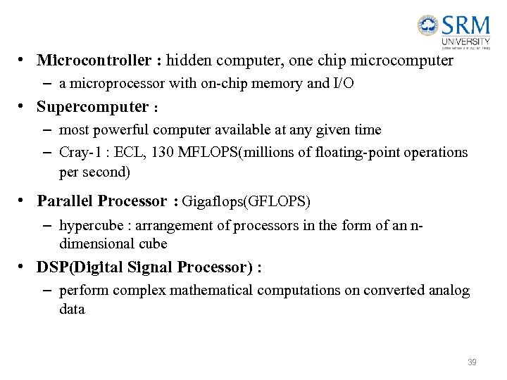 • Microcontroller : hidden computer, one chip microcomputer – a microprocessor with on-chip memory and I/O • Supercomputer : – most powerful computer available at any given time – Cray-1 : ECL, 130 MFLOPS(millions of floating-point operations per second) • Parallel Processor : Gigaflops(GFLOPS) – hypercube : arrangement of processors in the form of an ndimensional cube • DSP(Digital Signal Processor) : – perform complex mathematical computations on converted analog data 39
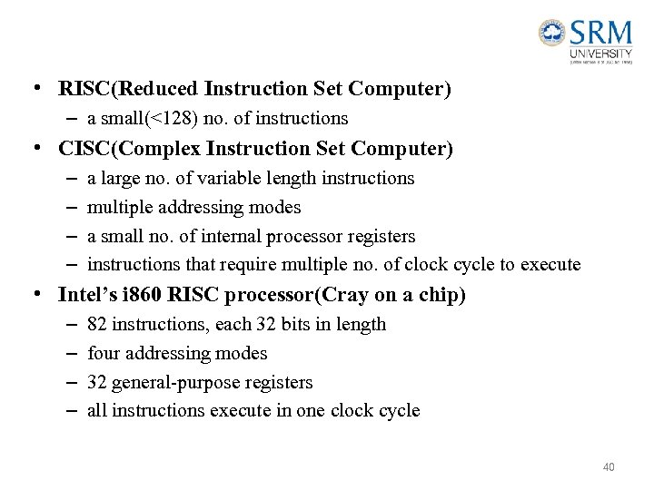 • RISC(Reduced Instruction Set Computer) – a small(<128) no. of instructions • CISC(Complex Instruction Set Computer) – – a large no. of variable length instructions multiple addressing modes a small no. of internal processor registers instructions that require multiple no. of clock cycle to execute • Intel’s i 860 RISC processor(Cray on a chip) – – 82 instructions, each 32 bits in length four addressing modes 32 general-purpose registers all instructions execute in one clock cycle 40
 41
41
 42
42
 8086 (1978) • 20 -bit address bus : 1 M byte(1024 Kbytes) memory • instruction : over 20, 000 variation – 4004 : 45, 8085 : 246 • A separate BIU and EU – Fetch and Execute instruction simultaneously • 16 -bit Internal processor registers – with the ability to access the high and low 8 bits separately if desired • hardware multiply and divide built in • support for an external math coprocessor – perform floating-point math operations as much as 100 times faster than the processor alone via software emulation 43
 44
44
 45
45
 8088 • 8086(1978) : 16 -bit data bus – requirement of two separate 8 -bit memory banks to supply its 16 -bit data bus – quite expensive memory chip at the time • 8088(1979) : external 8 -bit data bus • IBM announced the PC : 1981. 8 – 8088, 16 K memory(expandable 64 K), 4. 77 MHz(clock speed) – PC standard 46
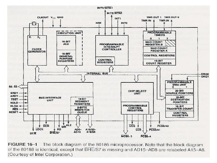
 80186/80188 • High-Integration CPUs – schematic diagram for IBM’s original PC • 8088 microprocessor • several additional chips are required – 80186 = 8086 + several additional chips • • • added 9 new instructions clock generator programmable timer programmable interrupt controller circuitry to select the I/O devices 47
 48
48
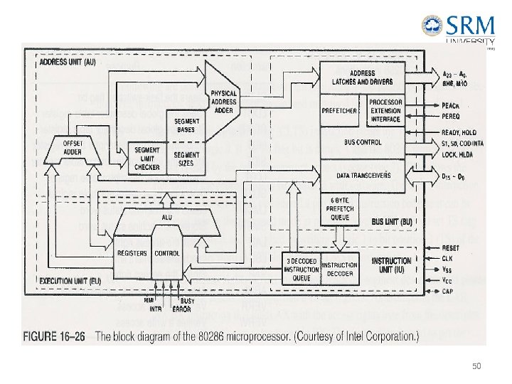
 80286 • • (1982) some instruction executed : 250 ns(4. 0 MIPS) at 8 MHz 24 -bit address bus : 16 M byte memory added 16 new instructions Real Mode: 1 st powered on – functions exactly like an 8086 – uses only its 20 least significant address lines(1 M) • Protected : • A “Fatal Flaw” ? – once switched to Protected mode, should not be able to switch back to Real mode – 286 chips are operated in Real mode and thus function only as fast 8086 s • IBM AT(advanced technology) Computer : 1984 49
 50
50
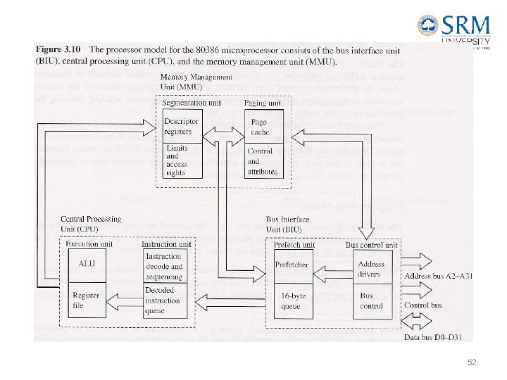
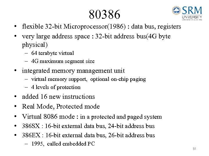 80386 • flexible 32 -bit Microprocessor(1986) : data bus, registers • very large address space : 32 -bit address bus(4 G byte physical) – 64 terabyte virtual – 4 G maximum segment size • integrated memory management unit – virtual memory support, optional on-chip paging – 4 levels of protection • added 16 new instructions • Real Mode, Protected mode • Virtual 8086 mode : in a protected and paged system • 386 SX : 16 -bit external data bus, 24 -bit address bus • 386 EX : 16 -bit external data bus, 26 -bit address bus – 1995, called embedded PC 51
 52
52
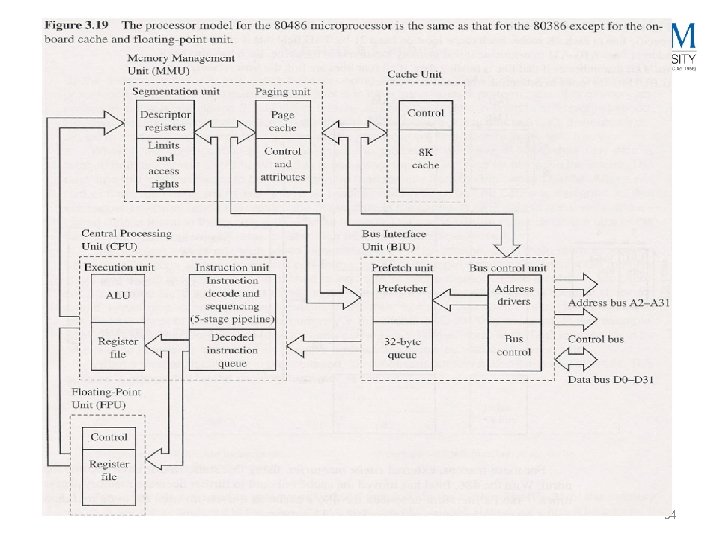
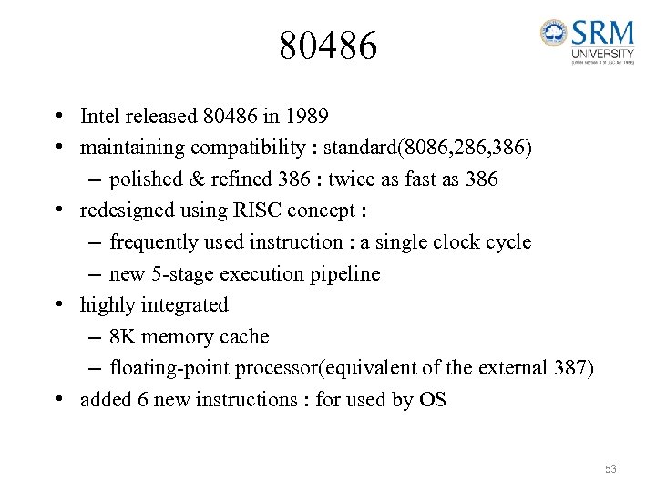 80486 • Intel released 80486 in 1989 • maintaining compatibility : standard(8086, 286, 386) – polished & refined 386 : twice as fast as 386 • redesigned using RISC concept : – frequently used instruction : a single clock cycle – new 5 -stage execution pipeline • highly integrated – 8 K memory cache – floating-point processor(equivalent of the external 387) • added 6 new instructions : for used by OS 53
 54
54
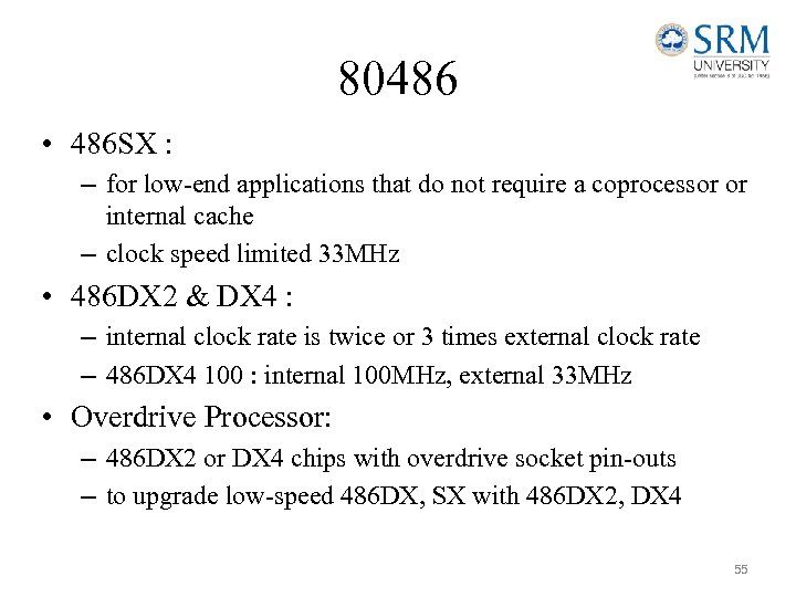 80486 • 486 SX : – for low-end applications that do not require a coprocessor or internal cache – clock speed limited 33 MHz • 486 DX 2 & DX 4 : – internal clock rate is twice or 3 times external clock rate – 486 DX 4 100 : internal 100 MHz, external 33 MHz • Overdrive Processor: – 486 DX 2 or DX 4 chips with overdrive socket pin-outs – to upgrade low-speed 486 DX, SX with 486 DX 2, DX 4 55
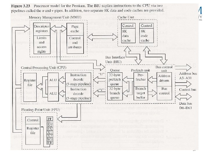
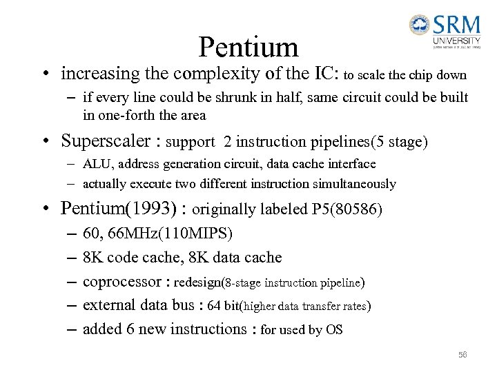 Pentium • increasing the complexity of the IC: to scale the chip down – if every line could be shrunk in half, same circuit could be built in one-forth the area • Superscaler : support 2 instruction pipelines(5 stage) – ALU, address generation circuit, data cache interface – actually execute two different instruction simultaneously • Pentium(1993) : originally labeled P 5(80586) – – – 60, 66 MHz(110 MIPS) 8 K code cache, 8 K data cache coprocessor : redesign(8 -stage instruction pipeline) external data bus : 64 bit(higher data transfer rates) added 6 new instructions : for used by OS 56
 57
57
 58
58
 59
59
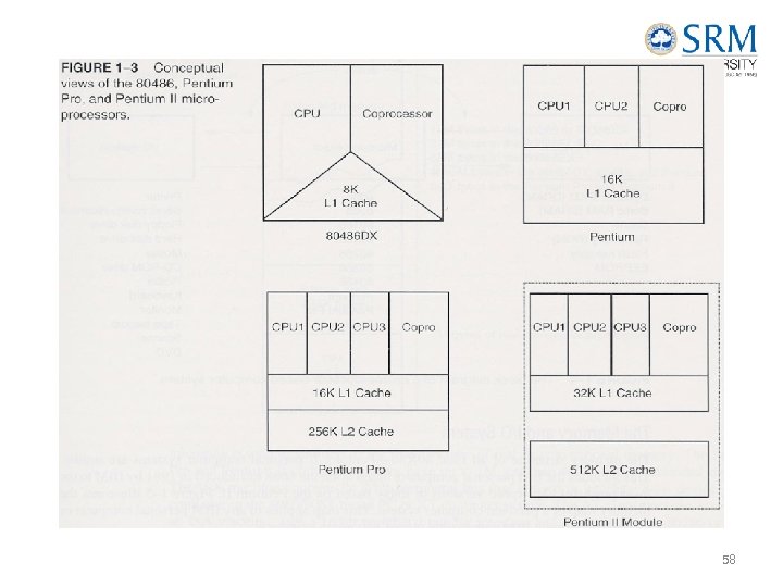
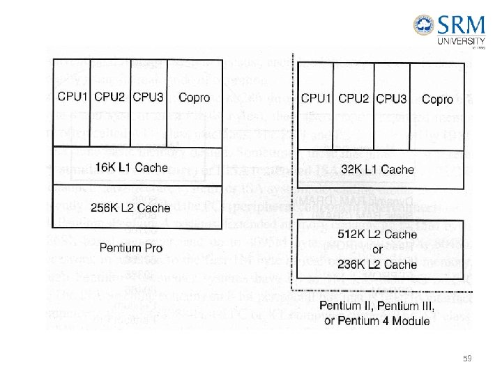
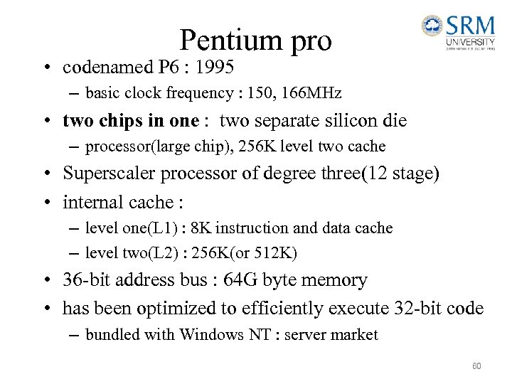 Pentium pro • codenamed P 6 : 1995 – basic clock frequency : 150, 166 MHz • two chips in one : two separate silicon die – processor(large chip), 256 K level two cache • Superscaler processor of degree three(12 stage) • internal cache : – level one(L 1) : 8 K instruction and data cache – level two(L 2) : 256 K(or 512 K) • 36 -bit address bus : 64 G byte memory • has been optimized to efficiently execute 32 -bit code – bundled with Windows NT : server market 60
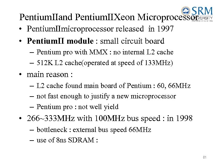 PentiumⅡand PentiumⅡXeon Microprocessor • PentiumⅡmicroprocessor released in 1997 • PentiumⅡ module : small circuit board – Pentium pro with MMX : no internal L 2 cache – 512 K L 2 cache(operated at speed of 133 MHz) • main reason : – L 2 cache found main board of Pentium : 60, 66 MHz – not fast enough to justify a new microprocessor – Pentium pro : not well yield • 266~333 MHz with 100 MHz bus speed : in 1998 – bottleneck : external bus speed 66 MHz – use of 8 ns SDRAM : 61
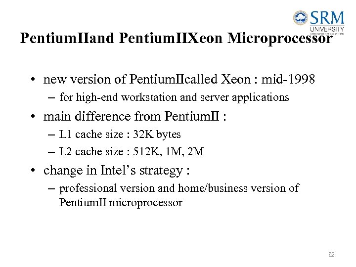 PentiumⅡand PentiumⅡXeon Microprocessor • new version of PentiumⅡcalled Xeon : mid-1998 – for high-end workstation and server applications • main difference from PentiumⅡ : – L 1 cache size : 32 K bytes – L 2 cache size : 512 K, 1 M, 2 M • change in Intel’s strategy : – professional version and home/business version of PentiumⅡ microprocessor 62
 Pentium Ⅲ Microprocessor • 1. used faster core than PentiumⅡ – is still P 6 or Pentium processor • 2. Two version : – bus speed : 100 MHz – 1. slot 1 version mounted on a plastic cartridge – 512 K cache : one-half the clock speed – 2. socket 370 version called flip-chip : looks like the older Pentium package → Intel claim cost less – 256 K cache : clock speed • 3. clock frequency : 1 GHz 63
 Pentium 4 Microprocessor • • release in late 2000 : used Intel P 6 architecture main difference : 1. clock speed : 1. 3, 1. 4, 1. 5 GHz 2. support to use RAMBUS memory technology – DDR(double-data-rate) SDRAM : both edge • 3. interconnection : from aluminum to copper – copper : is better conductor → increase clock frequency – bus speed : from current max. of 133 MHz to 200 MHz or higher 64
 The Future of Microprocessors • no one can really make accurate prediction : – success of Intel family should continue for quite a few years • what may occur is : will occur – a change to RISC technology, – but more likely a change to a new technology being developed jointly by Intel and Hewlett-Packard • new technology : – even will embody CISC instruction set of 80 X 86 family , – so that software for system will survive • basic premise behind this technology : many – will communicate directly with each other, allowing parallel processing without any change to instruction set or program 65
 • Double-clocked Pentium at 120 MHz and 133 MHz, also available. – fastest version produced 233 MHz Pentium a three and one-half clocked version • Cache size was increased to 16 K bytes from the 8 K cache found in 80486. • 8 K-byte instruction cache and data cache. • Memory system up to 4 G bytes. • Data bus width increased to a full 64 bits. • Data bus transfer speed 60 MHz or 66 MHz. – depending on the version of the Pentium 66
 • Wider data bus width accommodated doubleprecision floating-point numbers used in highspeed, vector-generated graphical displays. – should allow virtual reality software and video to operate at more realistic rates • Widened data bus and higher speed allow fullframe video displays at scan rates of 30 Hz or higher. – comparable to commercial television 67
 • Recent Pentium versions also included additional instructions. – multimedia extensions, or MMX instructions • Intel hoped MMX would be widely used – few software companies have used – no high-level language support for instructions • Over. Drive (P 24 T) for older 80486 systems. • 63 MHz version upgrades 80486 DX 2 50 MHz systems; 83 MHz upgrades 66 MHz systems. – system performs somewhere between a 66 MHz Pentium and a 75 MHz Pentium 68
 • Pentium Over. Drive represents ideal upgrade path from the 80486 to the Pentium. – executes two instructions not dependent on each other, simultaneously per clocking period – dual integer processors most ingenious feature – contains two independent internal integer processors called superscaler technology • Jump prediction speeds execution of program loops; internal floating-point coprocessor handles floating-point data. • These portend continued success for Intel. 69
 • Intel may allow Pentium to replace some RISC (reduced instruction set computer) machines. • Some newer RISC processors execute more than one instruction per clock. – through superscaler technology • Motorola, Apple, and IBM produce Power. PC, a RISC with two integer units and a floating-point unit. – boosts Macintosh performance, but slow to efficiently emulate Intel microprocessors 70
 • Currently 6 million Apple Macintosh systems • 260 million personal computers based on Intel microprocessors. • 1998 reports showed 96% of all PCs shipped with the Windows operating system. • Apple computer replaced Power. PC with the Intel Pentium in most of its computer systems. – appears that Power. PC could not keep pace with the Pentium line from Intel 71
 • To compare speeds of microprocessors, Intel devised the i. COMP- rating index. – composite of SPEC 92, ZD Bench, Power Meter • The i. COMP 1 rating index is used to rate the speed of all Intel microprocessors through the Pentium. • Figure 1– 2 shows relative speeds of the 80386 DX 25 MHz version through the Pentium 233 MHz version. 72
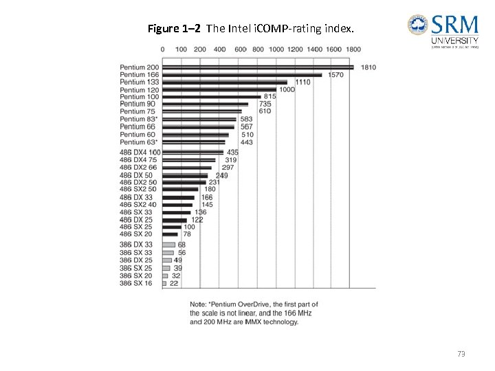 Figure 1– 2 The Intel i. COMP-rating index. 73
 • Since release of Pentium Pro and Pentium II, Intel has switched to the i. COMP 2 - rating. – scaled by a factor of 10 from the i. COMP 1 index • Figure 1– 3 shows i. COMP 2 index listing the Pentium III at speeds up to 1000 MHz. • Figure 1– 4 shows SYSmark 2002 for the Pentium III and Pentium 4. • Intel has not released benchmarks that compare versions of the microprocessor since the SYSmark 2002. – newer available do not compare versions 74
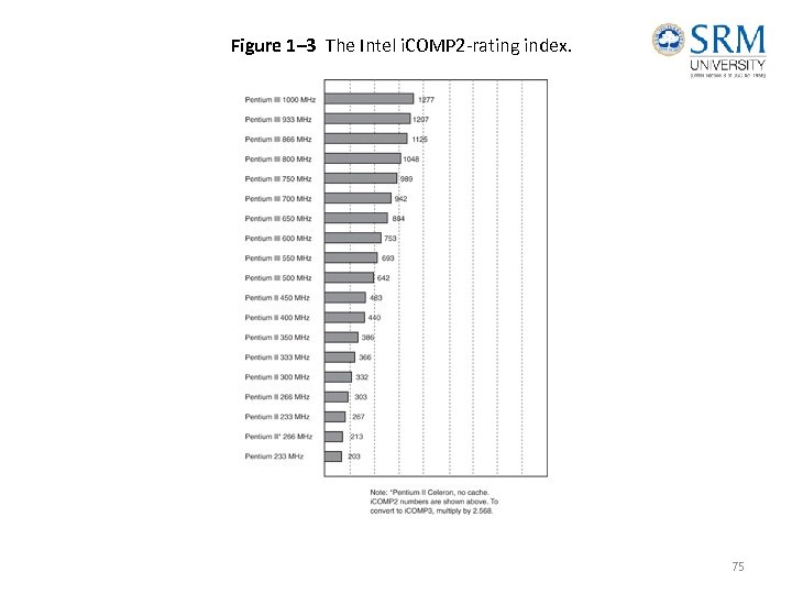 Figure 1– 3 The Intel i. COMP 2 -rating index. 75
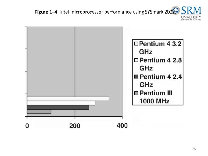 Figure 1– 4 Intel microprocessor performance using SYSmark 2002. 76
 Pentium Processor • A recent entry, formerly named the P 6. • 21 million transistors, integer units, floating-point unit, clock frequency 150 and 166 MHz • Internal 16 K level-one (L 1) cache. – 8 K data, 8 K for instructions – Pentium Pro contains 256 K level-two (L 2) cache • Pentium Pro uses three execution engines, to execute up to three instructions at a time. – can conflict and still execute in parallel 77
 • Pentium Pro optimized to efficiently execute 32 bit code. – often bundled with Windows NT rather than normal versions of Windows 95 – Intel launched Pentium Pro for server market • Pentium Pro can address 4 G-byte or a 64 G-byte memory system. – 36 -bit address bus if configured for a 64 G memory system 78
 Pentium II and Pentium Xeon Microprocessors • Pentium II, released 1997, represents new direction for Intel. • Intel has placed Pentium II on a small circuit board, instead of being an integrated circuit. – L 2 cache on main circuit board of not fast enough to function properly with Pentium II • Microprocessor on the Pentium II module actually Pentium Pro with MMX extensions. 79
 • In 1998 Intel changed Pentium II bus speed. – newer Pentium II uses a 100 MHz bus speed • Higher speed memory bus requires 8 ns SDRAM. – replaces 10 ns SDRAM with 66 MHz bus speed 80
 • Intel announced Xeon in mid-1998. – specifically designed for high-end workstation and server applications • Xeon available with 32 K L 1 cache and L 2 cache size of 512 K, 1 M, or 2 M bytes. • Xeon functions with the 440 GX chip set. • Also designed to function with four Xeons in the same system, similar to Pentium Pro. • Newer product represents strategy change. – Intel produces a professional and home/business version of the Pentium II 81
 Pentium III Microprocessor • Faster core than Pentium II; still a P 6 or Pentium Pro processor. • Available in slot 1 version mounted on a plastic cartridge. • Also socket 370 version called a flip-chip which looks like older Pentium package. • Pentium III available with clock frequencies up to 1 GHz. 82
 • Slot 1 version contains a 512 K cache; flip-chip version contains 256 K cache. • Flip-chip version runs at clock speed; Slot 1 cache version runs at one-half clock speed. • Both versions use 100 Mhz memory bus. – Celeron memory bus clock speed 66 MHz • Front side bus connection, microprocessor to memory controller, PCI controller, and AGP controller, now either 100 or 133 MHz. – this change has improved performance – memory still runs at 100 MHz 83
 Pentium 4 and Core 2 Microprocessors • Pentium 4 first made available in late 2000. – most recent version of Pentium called Core 2 – uses Intel P 6 architecture • Pentium 4 available to 3. 2 GHz and faster. – supporting chip sets use RAMBUS or DDR memory in place of SDRAM technology • Core 2 is available at speeds of up to 3 GHz. – improvement in internal integration, at present the 0. 045 micron or 45 nm technology 84
 • A likely change is a shift from aluminum to copper interconnections inside the microprocessor. • Copper is a better conductor. – should allow increased clock frequencies – especially true now that a method for using copper has surfaced at IBM • Another event to look for is a change in the speed of the front side bus. – increase beyond current maximum 1033 MHz 85
 Pentium 4 and Core 2, 64 -bit and Multiple Core Microprocessors • Recent modifications to Pentium 4 and Core 2 include a 64 -bit core and multiple cores. • 64 -bit modification allows address of over 4 G bytes of memory through a 64 -bit address. – 40 address pins in these newer versions allow up to 1 T (terabytes) of memory to be accessed • Also allows 64 -bit integer arithmetic. – less important than ability to address more memory 86
 • Biggest advancement is inclusion of multiple cores. – each core executes a separate task in a program • Increases speed of execution if program is written to take advantage of multiple cores. – called multithreaded applications • Intel manufactures dual and quad core versions; number of cores will likely increase to eight or even sixteen. 87
 • Multiple cores are current solution to providing faster microprocessors. • Intel recently demonstrated Core 2 containing 80 cores, using 45 nm fabrication technology. • Intel expects to release an 80 -core version some time in the next 5 years. • Fabrication technology will become slightly smaller with 35 nm and possibly 25 nm technology. 88
 The Future of Microprocessors • No one can make accurate predictions. • Success of Intel should continue. • Change to RISC technology may occur; more likely improvements to new hyper-threading technology. – joint effort by Intel and Hewlett-Packard • New technology embodies CISC instruction set of 80 X 86 family. – software for the system will survive 89
 • Basic premise is many microprocessors communicate directly with each other. – allows parallel processing without any change to the instruction set or program • Current superscaler technology uses many microprocessors; all share same register set. – new technology contains many microprocessors – each contains its own register set linked with the other microprocessors’ registers • Offers true parallel processing without writing any special program. 90
 • In 2002, Intel released a new architecture 64 bits in width with a 128 -bit data bus. • Named Itanium; joint venture called EPIC (Explicitly Parallel Instruction Computing) of Intel and Hewlett-Packard. • The Itanium architecture allows greater parallelism than traditional architectures. • 128 general-purpose integer and 128 floatingpoint registers; 64 predicate registers. • Many execution units to ensure enough hardware resources for software. 91
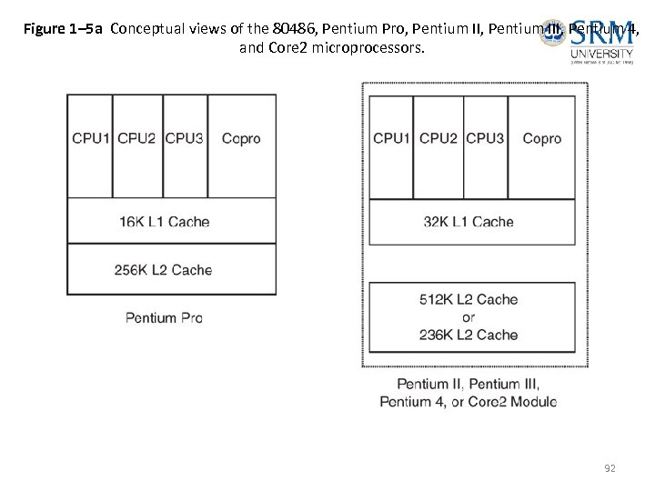 Figure 1– 5 a Conceptual views of the 80486, Pentium Pro, Pentium III, Pentium 4, and Core 2 microprocessors. 92
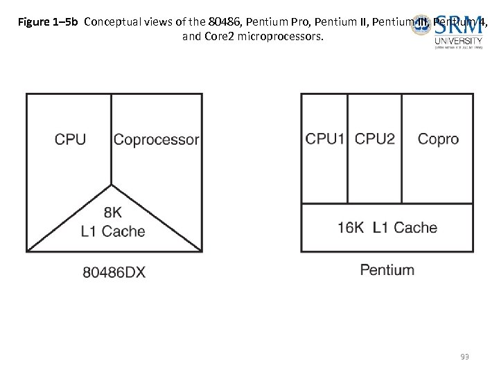 Figure 1– 5 b Conceptual views of the 80486, Pentium Pro, Pentium III, Pentium 4, and Core 2 microprocessors. 93
 • Clock frequencies seemed to have peaked. • Surge to multiple cores has begun. • Memory speed a consideration. – speed of dynamic RAM memory has not changed for many years. • Push to static RAM memory will eventually. increase the performance of the PC. – main problem with large static RAM is heat – static RAM operates 50 times faster than dynamic RAM 94
 • Speed of mass storage another problem. – transfer speed of hard disk drives has changed little in past few years – new technology needed for mass storage • Flash memory could be solution. – write speed comparable to hard disk memory • Flash memory could store the operation system for common applications. – would allow operating system to load in a second or two instead of many seconds now required 95
 3. THE MICROPROCESSOR-BASED PERSONAL COMPUTER SYSTEM • Computers have undergone many changes recently. • Machines that once filled large areas reduced to small desktop computer systems because of the microprocessor. – although compact, they possess computing power only dreamed of a few years ago 96
 • Figure 1– 6 shows block diagram of the personal computer. • Applies to any computer system, from early mainframe computers to the latest systems. • Diagram composed of three blocks interconnected by buses. – a bus is the set of common connections that carry the same type of information 97
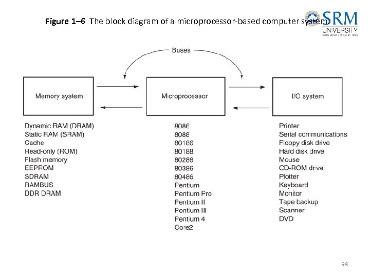 Figure 1– 6 The block diagram of a microprocessor-based computer system. 98
 The Memory and I/O System • Memory structure of all Intel-based personal computers similar. • Figure 1– 7 illustrates memory map of a personal computer system. • This map applies to any IBM personal computer. – also any IBM-compatible clones in existence 99
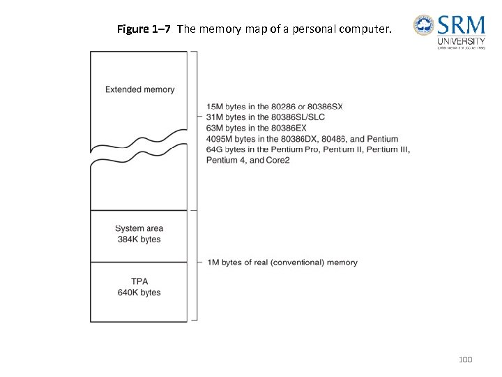 Figure 1– 7 The memory map of a personal computer. 100
 • Main memory system divided into three parts: – TPA (transient program area) – system area – XMS (extended memory system) • Type of microprocessor present determines whether an extended memory system exists. • First 1 M byte of memory often called the real or conventional memory system. – Intel microprocessors designed to function in this area using real mode operation 101
 • 80286 through the Core 2 contain the TPA (640 K bytes) and system area (384 K bytes). – also contain extended memory – often called AT class machines • The PS/l and PS/2 by IBM are other versions of the same basic memory design. • Also referred to as ISA (industry standard architecture) or EISA (extended ISA). • The PS/2 referred to as a micro-channel architecture or ISA system. – depending on the model number 102
 • Pentium and ATX class machines feature addition of the PCI (peripheral component interconnect) bus. – now used in all Pentium through Core 2 systems • Extended memory up to 15 M bytes in the 80286 and 80386 SX; 4095 M bytes in 80486 80386 DX, Pentium microprocessors. • The Pentium Pro through Core 2 computer systems have up to 1 M less than 4 G or 1 M less than 64 G of extended memory. • Servers tend to use the larger memory map. 103
 • Many 80486 systems use VESA local, VL bus to interface disk and video to the microprocessor at the local bus level. – allows 32 -bit interfaces to function at same clocking speed as the microprocessor – recent modification supporting 64 -bit data bus has generated little interest • ISA/EISA standards function at 8 MHz. • PCI bus is a 32 - or 64 -bit bus. – specifically designed to function with the Pentium through Core 2 at a bus speed of 33 MHz. 104
 • Three newer buses have appeared. • USB (universal serial bus). – intended to connect peripheral devices to the microprocessor through a serial data path and a twisted pair of wires • Data transfer rates are 10 Mbps for USB 1. • Increase to 480 Mbps in USB 2. 105
 • AGP (advanced graphics port) for video cards. • The port transfers data between video card and microprocessor at higher speeds. – 66 MHz, with 64 -bit data path • Latest AGP speed 8 X or 2 G bytes/second. – video subsystem change made to accommodate new DVD players for the PC. 106
 • Latest new buses are serial ATA interface (SATA) for hard disk drives; PCI Express bus for the video card. • The SATA bus transfers data from PC to hard disk at rates of 150 M bytes per second; 300 M bytes for SATA-2. – serial ATA standard will eventually reach speeds of 450 M bytes per second • PCI Express bus video cards operate at 16 X speeds today. 107
 The TPA • The transient program area (TPA) holds the DOS (disk operating system) operating system; other programs that control the computer system. – the TPA is a DOS concept and not really applicable in Windows – also stores any currently active or inactive DOS application programs – length of the TPA is 640 K bytes 108
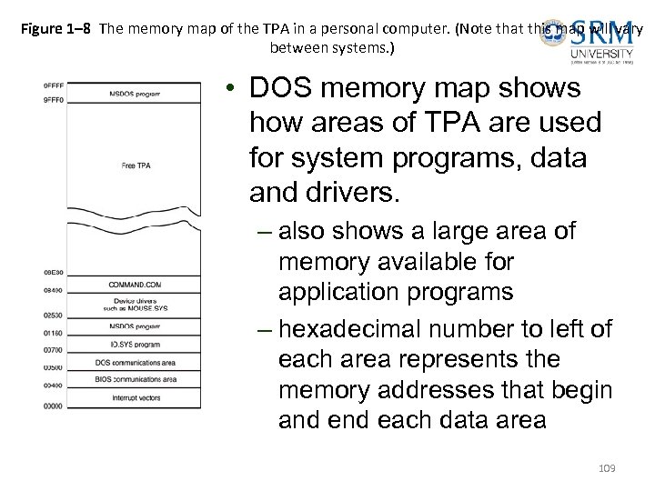 Figure 1– 8 The memory map of the TPA in a personal computer. (Note that this map will vary between systems. ) • DOS memory map shows how areas of TPA are used for system programs, data and drivers. – also shows a large area of memory available for application programs – hexadecimal number to left of each area represents the memory addresses that begin and each data area 109
 • Hexadecimal memory addresses number each byte of the memory system. – a hexadecimal number is a number represented in radix 16 or base 16 – each digit represents a value from 0 to 9 and from A to F • Often a hexadecimal number ends with an H to indicate it is a hexadecimal value. – 1234 H is 1234 hexadecimal – also represent hexadecimal data as 0 xl 234 for a 1234 hexadecimal 110
 • Interrupt vectors access DOS, BIOS (basic I/O system), and applications. • Areas contain transient data to access I/O devices and internal features of the system. – these are stored in the TPA so they can be changed as DOS operates 111
 • The IO. SYS loads into the TPA from the disk whenever an MSDOS system is started. • IO. SYS contains programs that allow DOS to use keyboard, video display, printer, and other I/O devices often found in computers. • The IO. SYS program links DOS to the programs stored on the system BIOS ROM. 112
 • Drivers are programs that control installable I/O devices. – mouse, disk cache, hand scanner, CD-ROM memory (Compact Disk Read-Only Memory), DVD (Digital Versatile Disk), or installable devices, as well as programs • Installable drivers control or drive devices or programs added to the computer system. • DOS drivers normally have an extension of. SYS; MOUSE. SYS. • DOS version 3. 2 and later files have an extension of. EXE; EMM 386. EXE. 113
 • Though not used by Windows, still used to execute DOS applications, even with Win XP. • Windows uses a file called SYSTEM. INI to load drivers used by Windows. • Newer versions of Windows have a registry added to contain information about the system and the drivers used. • You can view the registry with the REGEDIT program. 114
 • COMMAND. COM (command processor) controls operation of the computer from the keyboard when operated in the DOS mode. • COMMAND. COM processes DOS commands as they are typed from the keyboard. • If COMMAND. COM is erased, the computer cannot be used from the keyboard in DOS mode. – never erase COMMAND. COM, IO. SYS, or MSDOS. SYS to make room for other software – your computer will not function 115
 The System Area • Smaller than the TPA; just as important. • The system area contains programs on read-only (ROM) or flash memory, and areas of read/write (RAM) memory for data storage. • Figure 1– 9 shows the system area of a typical personal computer system. • As with the map of the TPA, this map also includes the hexadecimal memory addresses of the various areas. 116
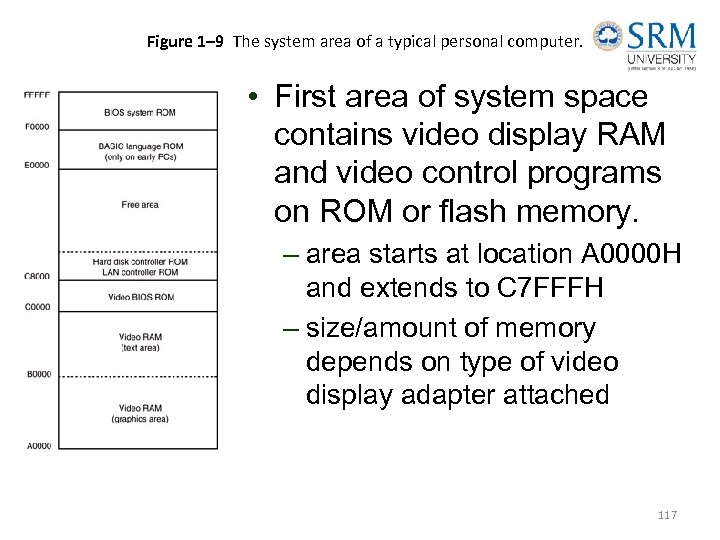 Figure 1– 9 The system area of a typical personal computer. • First area of system space contains video display RAM and video control programs on ROM or flash memory. – area starts at location A 0000 H and extends to C 7 FFFH – size/amount of memory depends on type of video display adapter attached 117
 • Display adapters generally have video RAM at A 0000 H–AFFFFH. – stores graphical or bit-mapped data • Memory at B 0000 H–BFFFFH stores text data. • The video BIOS on a ROM or flash memory, is at locations C 0000 H–C 7 FFFH. – contains programs to control DOS video display • C 8000 H–DFFFFH is often open or free. – used for expanded memory system (EMS) in PC or XT system; upper memory system in an AT 118
 • Expanded memory system allows a 64 K-byte page frame of memory for use by applications. – page frame (D 0000 H - DFFFFH) used to expand memory system by switching in pages of memory from EMS into this range of memory addresses • Locations E 0000 H–EFFFFH contain cassette BASIC on ROM found in early IBM systems. – often open or free in newer computer systems • Video system has its own BIOS ROM at location C 0000 H. 119
 • System BIOS ROM is located in the top 64 K bytes of the system area (F 0000 H–FFFFFH). – controls operation of basic I/O devices connected to the computer system – does not control operation of video • The first part of the system BIOS (F 0000 H–F 7 FFFH) often contains programs that set up the computer. • Second part contains procedures that control the basic I/O system. 120
 Windows Systems • Modern computers use a different memory map with Windows than DOS memory maps. • The Windows memory map in Figure 1– 10 has two main areas; a TPA and system area. • The difference between it and the DOS memory map are sizes and locations of these areas. 121
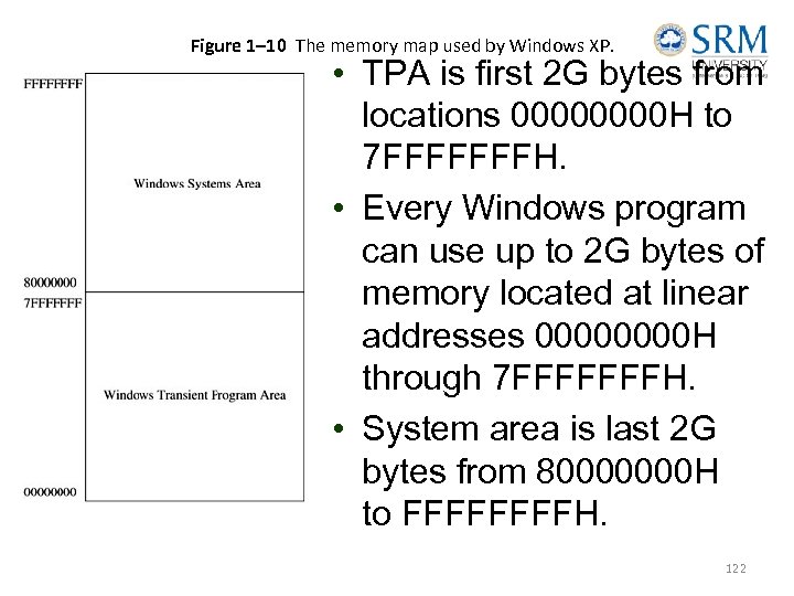 Figure 1– 10 The memory map used by Windows XP. • TPA is first 2 G bytes from locations 0000 H to 7 FFFFFFFH. • Every Windows program can use up to 2 G bytes of memory located at linear addresses 0000 H through 7 FFFFFFFH. • System area is last 2 G bytes from 80000000 H to FFFFH. 122
 • Memory system physical map is much different. • Every process in a Windows Vista, XP, or 2000 system has its own set of page tables. • The process can be located anywhere in the memory, even in noncontiguous pages. • The operating system assigns physical memory to application. – if not enough exists, it uses the hard disk for any that is not available 123
 I/O Space • I/O devices allow the microprocessor to communicate with the outside world. • I/O (input/output) space in a computer system extends from I/O port 0000 H to port FFFFH. – I/O port address is similar to a memory address – instead of memory, it addresses an I/O device • Figure 1– 11 shows the I/O map found in many personal computer systems. 124
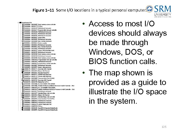 Figure 1– 11 Some I/O locations in a typical personal computer. • Access to most I/O devices should always be made through Windows, DOS, or BIOS function calls. • The map shown is provided as a guide to illustrate the I/O space in the system. 125
 • The area below I/O location 0400 H is considered reserved for system devices • Area available for expansion extends from I/O port 0400 H through FFFFH. • Generally, 0000 H - 00 FFH addresses main board components; 0100 H - 03 FFH handles devices located on plug-in cards or also on the main board. • The limitation of I/O addresses between 0000 and 03 FFH comes from original standards specified by IBM for the PC standard. 126
 The Microprocessor • Called the CPU (central processing unit). • The controlling element in a computer system. • Controls memory and I/O through connections called buses. – buses select an I/O or memory device, transfer data between I/O devices or memory and the microprocessor, control I/O and memory systems • Memory and I/O controlled via instructions stored in memory, executed by the microprocessor. 127
 • Microprocessor performs three main tasks: – data transfer between itself and the memory or I/O systems – simple arithmetic and logic operations – program flow via simple decisions • Power of the microprocessor is capability to execute billions of millions of instructions per second from a program or software (group of instructions) stored in the memory system. – stored programs make the microprocessor and computer system very powerful devices 128
 • Another powerful feature is the ability to make simple decisions based upon numerical facts. – a microprocessor can decide if a number is zero, positive, and so forth • These decisions allow the microprocessor to modify the program flow, so programs appear to think through these simple decisions. 129
 Buses • A common group of wires that interconnect components in a computer system. • Transfer address, data, & control information between microprocessor, memory and I/O. • Three buses exist for this transfer of information: address, data, and control. • Figure 1– 12 shows how these buses interconnect various system components. 130
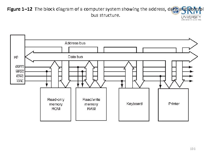 Figure 1– 12 The block diagram of a computer system showing the address, data, and control bus structure. 131
 • The address bus requests a memory location from the memory or an I/O location from the I/O devices. – if I/O is addressed, the address bus contains a 16 -bit I/O address from 0000 H through FFFFH. – if memory is addressed, the bus contains a memory address, varying in width by type of microprocessor. • 64 -bit extensions to Pentium provide 40 address pins, allowing up to 1 T byte of memory to be accessed. 132
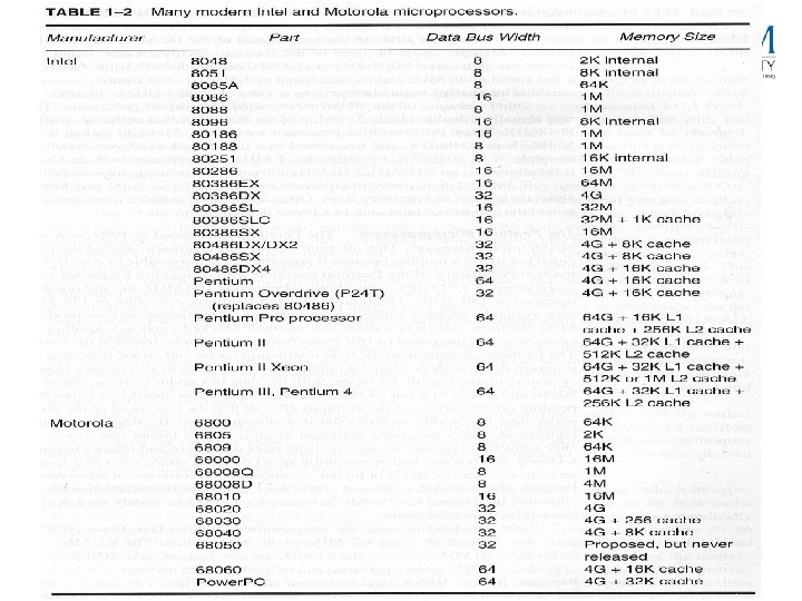
 • The data bus transfers information between the microprocessor and its memory and I/O address space. • Data transfers vary in size, from 8 bits wide to 64 bits wide in various Intel microprocessors. – 8088 has an 8 -bit data bus that transfers 8 bits of data at a time – 8086, 80286, 80386 SL, 80386 SX, and 80386 EX transfer 16 bits of data – 80386 DX, 80486 SX, and 80486 DX, 32 bits – Pentium through Core 2 microprocessors transfer 64 bits of data 133
 • Advantage of a wider data bus is speed in applications using wide data. • Figure 1– 13 shows memory widths and sizes of 8086 through Core 2 microprocessors. • In all Intel microprocessors family members, memory is numbered by byte. • Pentium through Core 2 microprocessors contain a 64 -bit-wide data bus. 134
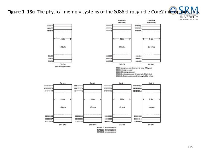 Figure 1– 13 a The physical memory systems of the 8086 through the Core 2 microprocessors. 135
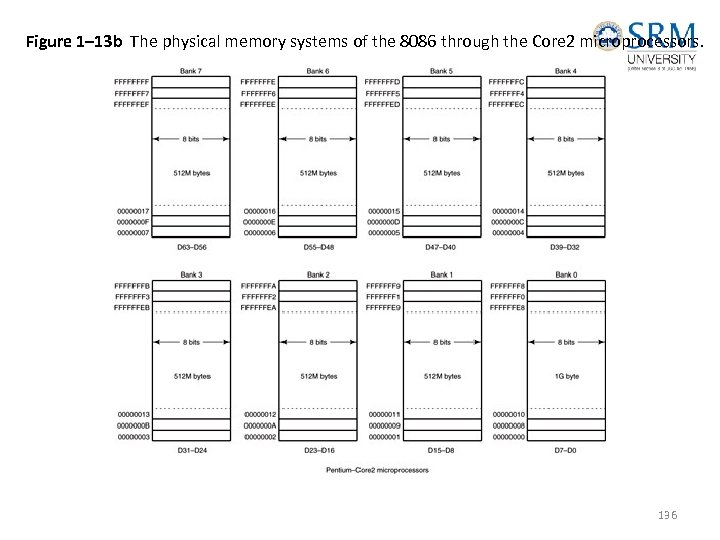 Figure 1– 13 b The physical memory systems of the 8086 through the Core 2 microprocessors. 136
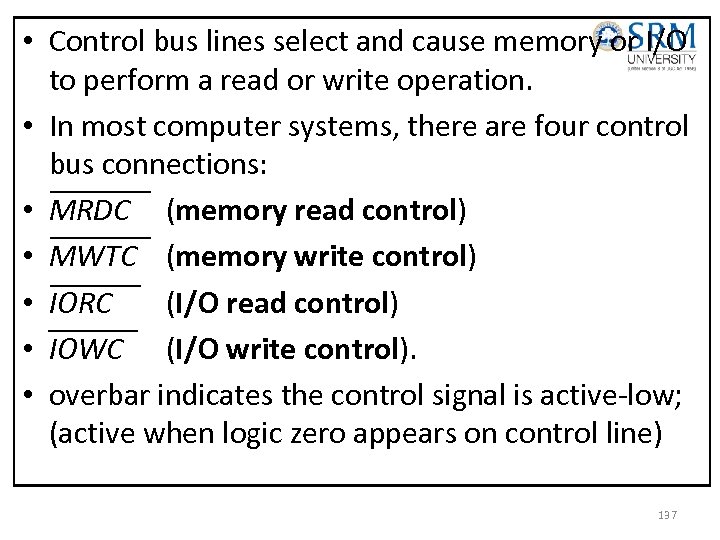 • Control bus lines select and cause memory or I/O to perform a read or write operation. • In most computer systems, there are four control bus connections: • MRDC (memory read control) • MWTC (memory write control) • IORC (I/O read control) • IOWC (I/O write control). • overbar indicates the control signal is active-low; (active when logic zero appears on control line) 137
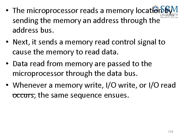 • The microprocessor reads a memory location by sending the memory an address through the address bus. • Next, it sends a memory read control signal to cause the memory to read data. • Data read from memory are passed to the microprocessor through the data bus. • Whenever a memory write, I/O write, or I/O read occurs, the same sequence ensues. 138
 Word-Sized Data • A word (16 -bits) is formed with two bytes of data. • The least significant byte always stored in the lowest-numbered memory location. • Most significant byte is stored in the highest. • This method of storing a number is called the little endian format. 139
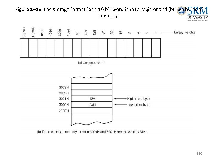 Figure 1– 15 The storage format for a 16 -bit word in (a) a register and (b) two bytes of memory. 140
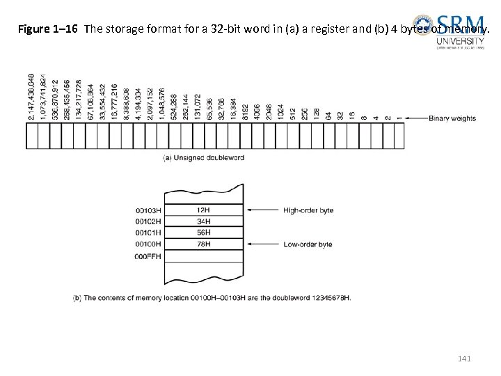 Figure 1– 16 The storage format for a 32 -bit word in (a) a register and (b) 4 bytes of memory. 141
 4. INTERNAL MICROPROCESSOR ARCHITECTURE • Before a program is written or instruction investigated, internal configuration of the microprocessor must be known. • In a multiple core microprocessor each core contains the same programming model. • Each core runs a separate task or thread simultaneously. 142
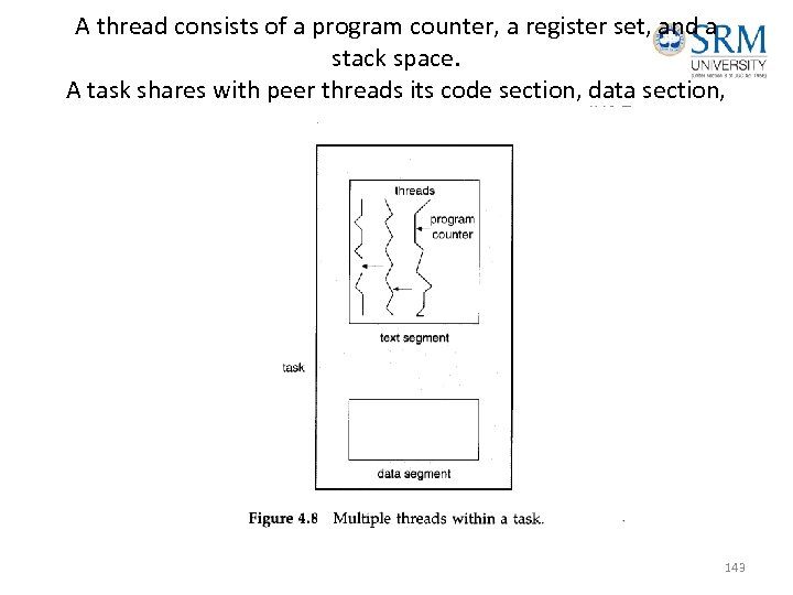 A thread consists of a program counter, a register set, and a stack space. A task shares with peer threads its code section, data section, and operating system resources 143
 The Programming Model • 8086 through Core 2 considered program visible. – registers are used during programming and are specified by the instructions • Other registers considered to be program invisible. – not addressable directly during applications programming 144
 • 80286 and above contain program-invisible registers to control and operate protected memory. – and other features of the microprocessor • 80386 through Core 2 microprocessors contain full 32 -bit internal architectures. • 8086 through the 80286 are fully upwardcompatible to the 80386 through Core 2. • Figure 2– 1 illustrates the programming model 8086 through Core 2 microprocessor. – including the 64 -bit extensions 145
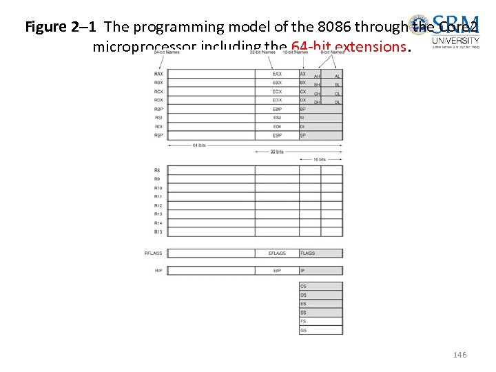 Figure 2– 1 The programming model of the 8086 through the Core 2 microprocessor including the 64 -bit extensions. 146
 Multipurpose Registers • RAX - a 64 -bit register (RAX), a 32 -bit register (accumulator) (EAX), a 16 -bit register (AX), or as either of two 8 -bit registers (AH and AL). • The accumulator is used for instructions such as multiplication, division, and some of the adjustment instructions. • Intel plans to expand the address bus to 52 bits to address 4 P (252~1015 =peta) bytes of memory. 147
 Address Space (Main Memory: RAM) • Address bus: 16 bit Address Space: 64 KBytes • Address bus: 20 bit Address Space: 1 MBytes Address bus: 32 bit Address Space: 4 GBytes Address bus: 34 bit Address Space: 16 GBytes • Address bus: 36 bit Address Space: 64 GBytes • Address bus: 38 bit Address Space: 256 GBytes • Address bus: 52 bit Address Space: 1015 Bytes 148
 • RBX, addressable as RBX, EBX, BH, BL. – BX register (base index) sometimes holds offset address of a location in the memory system in all versions of the microprocessor • RCX, as RCX, ECX, CH, or CL. – a (count) general-purpose register that also holds the count for various instructions • RDX, as RDX, EDX, DH, or DL. – a (data) general-purpose register – holds a part of the result from a multiplication or part of dividend before a division 149
 • RBP, as RBP, EBP, or BP. – points to a memory (base pointer) location for memory data transfers • RDI addressable as RDI, EDI, or DI. – often addresses (destination index) string destination data for the string instructions • RSI used as RSI, ESI, or SI. – the (source index) register addresses source string data for the string instructions – like RDI, RSI also functions as a generalpurpose register 150
 • R 8 - R 15 found in the Pentium 4 and Core 2 if 64 bit extensions are enabled. – data are addressed as 64 -, 32 -, 16 -, or 8 -bit sizes and are of general purpose • Most applications will not use these registers until 64 -bit processors are common. – the 8 -bit portion is the rightmost 8 -bit only – bits 8 to 15 are not directly addressable as a byte 151
 Special-Purpose Registers • Include RIP, RSP, and RFLAGS – segment registers include CS, DS, ES, SS, FS, and GS • RIP addresses the next instruction in a section of memory. – defined as (instruction pointer) a code segment • RSP addresses an area of memory called the stack. – the (stack pointer) stores data through this pointer 152
 • RFLAGS indicate the condition of the microprocessor and control its operation. • Figure 2– 2 shows the flag registers of all versions of the microprocessor. • Flags are upward-compatible from the 8086/8088 through Core 2. • The rightmost five and the overflow flag are changed by most arithmetic and logic operations. – although data transfers do not affect them 153
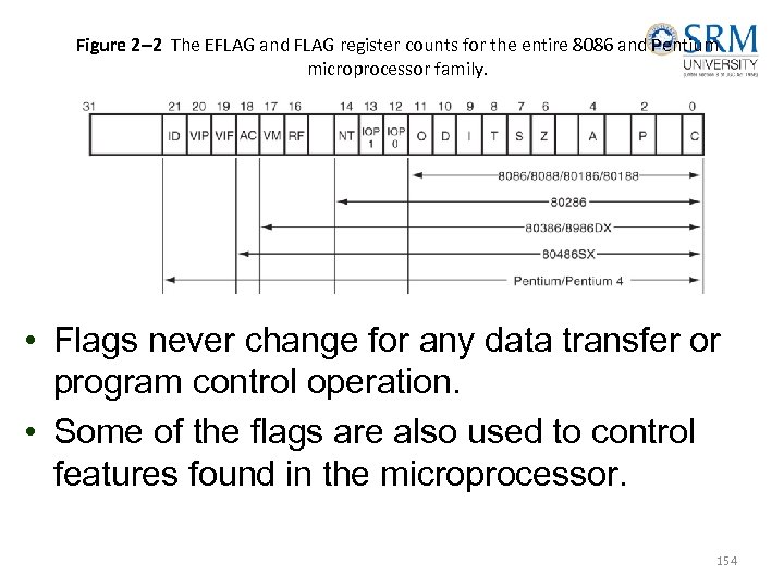 Figure 2– 2 The EFLAG and FLAG register counts for the entire 8086 and Pentium microprocessor family. • Flags never change for any data transfer or program control operation. • Some of the flags are also used to control features found in the microprocessor. 154
 • Flag bits, with a brief description of function. • C (carry) holds the carry after addition or borrow after subtraction. – also indicates error conditions • P (parity) is the count of ones in a number expressed as even or odd. Logic 0 for odd parity; logic 1 for even parity. – if a number contains three binary one bits, it has odd parity – if a number contains no one bits, it has even parity 155
 List of Each Flag bit, with a brief description of function. • C (carry) holds the carry after addition or borrow after subtraction. – also indicates error conditions • P (parity) is the count of ones in a number expressed as even or odd. Logic 0 for odd parity; logic 1 for even parity. – if a number contains three binary one bits, it has odd parity; If a number contains no one bits, it has even parity 156
 • A (auxiliary carry) holds the carry (half-carry) after addition or the borrow after subtraction between bit positions 3 and 4 of the result. • Z (zero) shows that the result of an arithmetic or logic operation is zero. • S (sign) flag holds the arithmetic sign of the result after an arithmetic or logic instruction executes. • T (trap) The trap flag enables trapping through an on-chip debugging feature. 157
 • I (interrupt) controls operation of the INTR (interrupt request) input pin. • D (direction) selects increment or decrement mode for the DI and/or SI registers. • O (overflow) occurs when signed numbers are added or subtracted. – an overflow indicates the result has exceeded the capacity of the machine 158
 • IOPL used in protected mode operation to select the privilege level for I/O devices. • NT (nested task) flag indicates the current task is nested within another task in protected mode operation. • RF (resume) used with debugging to control resumption of execution after the next instruction. • VM (virtual mode) flag bit selects virtual mode operation in a protected mode system. 159
 • AC, (alignment check) flag bit activates if a word or doubleword is addressed on a non-word or non -doubleword boundary. • VIF is a copy of the interrupt flag bit available to the Pentium 4–(virtual interrupt) • VIP (virtual) provides information about a virtual mode interrupt for (interrupt pending) Pentium. – used in multitasking environments to provide virtual interrupt flags 160
 • ID (identification) flag indicates that the Pentium microprocessors support the CPUID instruction. – CPUID instruction provides the system with information about the Pentium microprocessor 161
 Segment Registers • Generate memory addresses when combined with other registers in the microprocessor. • Four or six segment registers in various versions of the microprocessor. • A segment register functions differently in real mode than in protected mode. • Following is a list of each segment register, along with its function in the system. 162
 • CS (code) segment holds code (programs and procedures) used by the microprocessor. • DS (data) contains most data used by a program. – Data are accessed by an offset address or contents of other registers that hold the offset address • ES (extra) an additional data segment used by some instructions to hold destination data. 163
 • SS (stack) defines the area of memory used for the stack. – stack entry point is determined by the stack segment and stack pointer registers – the BP register also addresses data within the stack segment 164
 • FS and GS segments are supplemental segment registers available in 80386–Core 2 microprocessors. – allow two additional memory segments for access by programs • Windows uses these segments for internal operations, but no definition of their usage is available. 165
 5. REAL MODE MEMORY ADDRESSING • 80286 and above operate in either the real or protected mode. • Real mode operation allows addressing of only the first 1 M byte of memory space—even in Pentium 4 or Core 2 microprocessor. – the first 1 M byte of memory is called the real memory, conventional memory, or DOS memory system 166
 Segments and Offsets • All real mode memory addresses must consist of a segment address plus an offset address. – segment address defines the beginning address of any 64 K-byte memory segment – offset address selects any location within the 64 K byte memory segment • Figure 2– 3 shows how the segment plus offset addressing scheme selects a memory location. 167
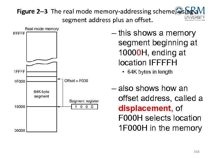 Figure 2– 3 The real mode memory-addressing scheme, using a segment address plus an offset. – this shows a memory segment beginning at 10000 H, ending at location IFFFFH • 64 K bytes in length – also shows how an offset address, called a displacement, of F 000 H selects location 1 F 000 H in the memory 168
 • Once the beginning address is known, the ending address is found by adding FFFFH. – because a real mode segment of memory is 64 K in length • The offset address is always added to the segment starting address to locate the data. • Segment and offset address is sometimes written as 1000: 2000. – a segment address of 1000 H; an offset of 2000 H 169
 Default Segment and Offset Registers • The microprocessor has rules that apply to segments whenever memory is addressed. – these define the segment and offset register combination • The code segment register defines the start of the code segment. • The instruction pointer locates the next instruction within the code segment. 170
 • Another of the default combinations is the stack. – stack data are referenced through the stack segment at the memory location addressed by either the stack pointer (SP/ESP) or the pointer (BP/EBP) • Figure 2– 4 shows a system that contains four memory segments. – a memory segment can touch or overlap if 64 K bytes of memory are not required for a segment 171
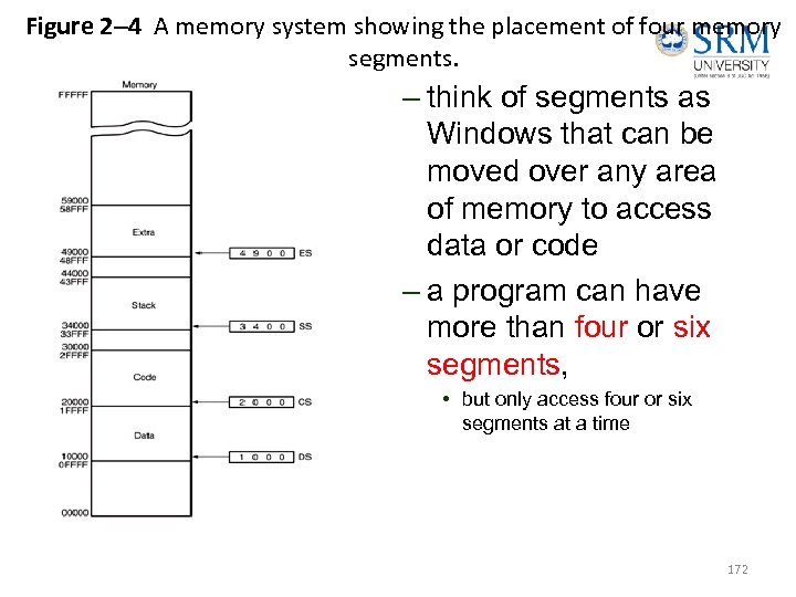 Figure 2– 4 A memory system showing the placement of four memory segments. – think of segments as Windows that can be moved over any area of memory to access data or code – a program can have more than four or six segments, • but only access four or six segments at a time 172
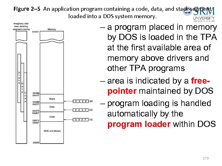 Figure 2– 5 An application program containing a code, data, and stack segment loaded into a DOS system memory. – a program placed in memory by DOS is loaded in the TPA at the first available area of memory above drivers and other TPA programs – area is indicated by a freepointer maintained by DOS – program loading is handled automatically by the program loader within DOS 173
 TPA • The transient program area (TPA) holds the DOS (disk operating system) operating system; other programs that control the computer system. 174
 Segment and Offset Addressing Scheme Allows Relocation • Segment plus offset addressing allows DOS programs to be relocated in memory. • A relocatable program is one that can be placed into any area of memory and executed without change. • Relocatable data are data that can be placed in any area of memory and used without any change to the program. 175
 • Because memory is addressed within a segment by an offset address, the memory segment can be moved to any place in the memory system without changing any of the offset addresses. • Only the contents of the segment register must be changed to address the program in the new area of memory. • Windows programs are written assuming that the first 2 G of memory are available for code and data. 176
 6. INTRO TO PROTECTED MODE MEMORY ADDRESSING • Allows access to data and programs located within & above the first 1 M byte of memory. • Protected mode is where Windows operates. • In place of a segment address, the segment register contains a selector that selects a descriptor from a descriptor table. • The descriptor describes the memory segment’s location, length, and access rights. 177
 Selectors and Descriptors • The descriptor is located in the segment register & describes the location, length, and access rights of the segment of memory. – it selects one of 8192 descriptors from one of two tables of descriptors • In protected mode, this segment number can address any memory location in the system for the code segment. • Indirectly, the register still selects a memory segment, but not directly as in real mode. 178
 • Global descriptors contain segment definitions that apply to all programs. • Local descriptors are usually unique to an application. – a global descriptor might be called a system descriptor, and local descriptor an application descriptor • Figure 2– 6 shows the format of a descriptor for the 80286 through the Core 2. – each descriptor is 8 bytes in length – global and local descriptor tables are a maximum of 64 K bytes in length 179
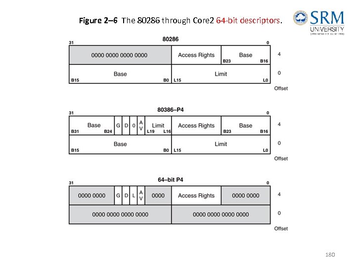 Figure 2– 6 The 80286 through Core 2 64 -bit descriptors. 180
 • The base address of the descriptor indicates the starting location of the memory segment. – the paragraph boundary limitation is removed in protected mode – segments may begin at any address • The G, or granularity bit allows a segment length of 4 K to 4 G bytes in steps of 4 K bytes. – 32 -bit offset address allows segment lengths of 4 G bytes – 16 -bit offset address allows segment lengths of 64 K bytes. 181
 • Operating systems operate in a 16 - or 32 -bit environment. • DOS uses a 16 -bit environment. • Most Windows applications use a 32 -bit environment called WIN 32. • MSDOS/PCDOS & Windows 3. 1 operating systems require 16 -bit instruction mode. • Instruction mode is accessible only in a protected mode system such as Windows XP Windows Vista Windows 7 Windows 8 ? ? ? . 182
 • The access rights byte controls access to the protected mode segment. – describes segment function in the system and allows complete control over the segment – if the segment is a data segment, the direction of growth is specified • If the segment grows beyond its limit, the operating system is interrupted, indicating a general protection fault. • You can specify whether a data segment can be written or is write-protected. 183
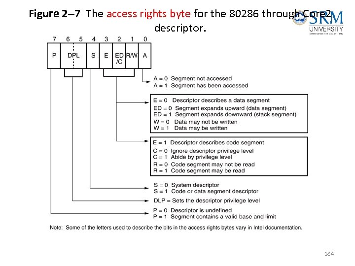 Figure 2– 7 The access rights byte for the 80286 through Core 2 descriptor. 184
 • Descriptors are chosen from the descriptor table by the segment register. – register contains a 13 -bit selector field, a table selector bit, and requested privilege level field • The TI bit selects either the global or the local descriptor table. • Requested Privilege Level (RPL) requests the access privilege level of a memory segment. – If privilege levels are violated, system normally indicates an application or privilege level violation 185
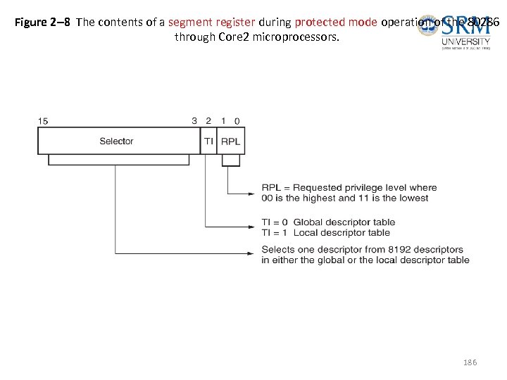 Figure 2– 8 The contents of a segment register during protected mode operation of the 80286 through Core 2 microprocessors. 186
 • Figure 2– 9 shows how the segment register, containing a selector, chooses a descriptor from the global descriptor table. • The entry in the global descriptor table selects a segment in the memory system. • Descriptor zero is called the null descriptor, must contain all zeros, and may not be used for accessing memory. 187
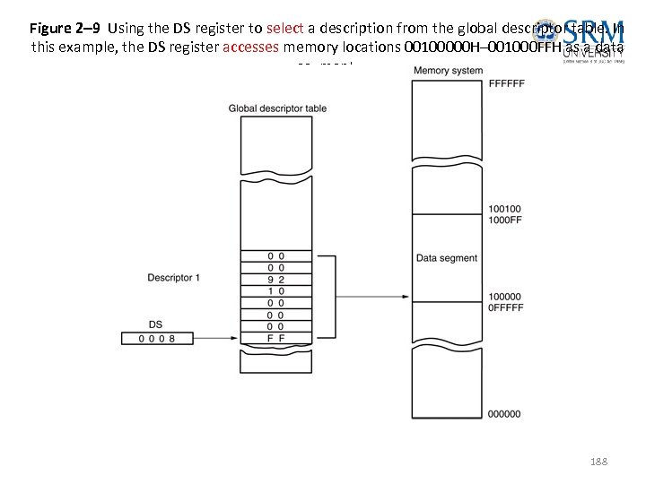 Figure 2– 9 Using the DS register to select a description from the global descriptor table. In this example, the DS register accesses memory locations 00100000 H– 001000 FFH as a data segment. 188
 Program-Invisible Registers • Global and local descriptor tables are found in the memory system. • To access & specify the table addresses, 80286– Core 2 contain program-invisible registers. – not directly addressed by software • Each segment register contains a program-invisible portion used in the protected mode. – often called cache memory because cache is any memory that stores information 189
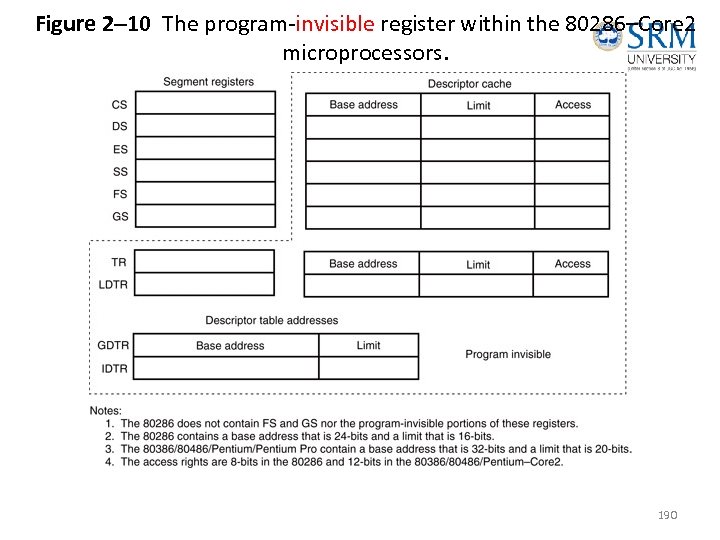 Figure 2– 10 The program-invisible register within the 80286–Core 2 microprocessors. 190
 • When a new segment number is placed in a segment register, the microprocessor accesses a descriptor table and loads the descriptor into the program-invisible portion of the segment register. – held there and used to access the memory segment until the segment number is changed • This allows the microprocessor to repeatedly access a memory segment without referring to the descriptor table. – hence the term cache 191
 • The GDTR (global descriptor table register) and IDTR (interrupt descriptor table register) contain the base address of the descriptor table and its limit. – when protected mode operation desired, address of the global descriptor table and its limit are loaded into the GDTR • The location of the local descriptor table is selected from the global descriptor table. – one of the global descriptors is set up to address the local descriptor table 192
 • To access the local descriptor table, the LDTR (local descriptor table register) is loaded with a selector. – selector accesses global descriptor table, & loads local descriptor table address, limit, & access rights into the cache portion of the LDTR • The TR (task register) holds a selector, which accesses a descriptor that defines a task. – a task is most often a procedure or application • Allows multitasking systems to switch tasks to another in a simple and orderly fashion. 193
 194
194


