438fa4b8937d3bc71214c610326ad9a1.ppt
- Количество слайдов: 19
 1 Micro Pattern Gas Detector Signal Characteristics, Frontend Electronics Specification Werner Riegler, CERN PH September 10 th 2007 Some very basic facts about signals and electronics that must not be forgotten when discussing Micro Pattern Detectors in relation to other detectors. W. Riegler/CERN
 2 Micro Pattern Gas Detectors ‘High’ Rate Capability ‘Excellent’ Time Resolution ‘Excellent’ Position Resolution Clearly all this cannot be achieved at the same time ‘Excellent’ results are achieved with conventional wire chambers: Rates of 2. 5 MHz/cm 2 Time resolution of 2 ns at 1 atm (<100 ps at low pressure) Position resolution of 15 μm. One has to be very specific about the quoted numbers. W. Riegler/CERN
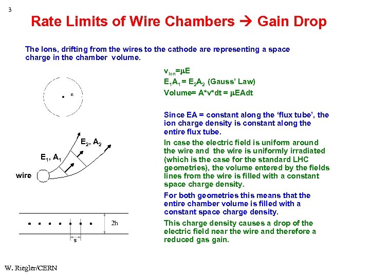 3 Rate Limits of Wire Chambers Gain Drop The Ions, drifting from the wires to the cathode are representing a space charge in the chamber volume. v. Ion= E E 1 A 1 = E 2 A 2 (Gauss’ Law) Volume= A*v*dt = EAdt E 2, A 2 E 1, A 1 wire W. Riegler/CERN Since EA = constant along the ‘flux tube’, the ion charge density is constant along the entire flux tube. In case the electric field is uniform around the wire and the wire is uniformly irradiated (which is the case for the standard LHC geometries), the volume entered by the fields lines from the wire is filled with a constant space charge density. For both geometries this means that the entire chamber volume is filled with a constant space charge density. This charge density causes a drop of the electric field near the wire and therefore a reduced gas gain.
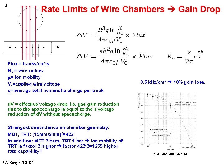 4 Rate Limits of Wire Chambers Gain Drop Flux = tracks/cm 2 s Ra = wire radius = ion mobility V 0=applied wire voltage q=average total avalanche charge per track 0. 5 k. Hz/cm 2 10% gain loss. d. V = effective voltage drop, i. e. gas gain reduction due to the spacecharge is equal to the a voltage reduction of d. V without spacecharge. Strongest dependence on chamber geometry. MDT, TRT: (15 mm/2 mm)3=422 In addition: MDT 3 bars, TRT 1 bar ion mobility of TRT is factor 3 higher factor 422*3=1265 higher rate capability ! W. Riegler/CERN NIMA 446(2000) 435 -43
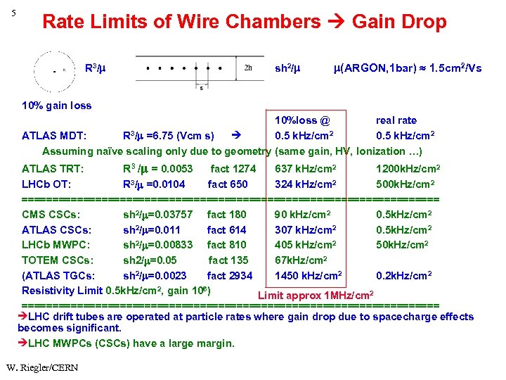 5 Rate Limits of Wire Chambers Gain Drop R 3/ sh 2/ (ARGON, 1 bar) 1. 5 cm 2/Vs 10% gain loss 10%loss @ real rate ATLAS MDT: R 3/ =6. 75 (Vcm s) 0. 5 k. Hz/cm 2 Assuming naïve scaling only due to geometry (same gain, HV, Ionization …) ATLAS TRT: R 3 / = 0. 0053 fact 1274 637 k. Hz/cm 2 1200 k. Hz/cm 2 LHCb OT: R 3/ =0. 0104 fact 650 324 k. Hz/cm 2 500 k. Hz/cm 2 ================================== CMS CSCs: sh 2/ =0. 03757 fact 180 90 k. Hz/cm 2 0. 5 k. Hz/cm 2 ATLAS CSCs: sh 2/ =0. 011 fact 614 307 k. Hz/cm 2 0. 5 k. Hz/cm 2 LHCb MWPC: sh 2/ =0. 00833 fact 810 405 k. Hz/cm 2 50 k. Hz/cm 2 TOTEM CSCs: sh 2/ =0. 05 fact 135 67 k. Hz/cm 2 (ATLAS TGCs: sh 2/ =0. 0023 fact 2934 1450 k. Hz/cm 2 0. 2 k. Hz/cm 2 Resistivity Limit 0. 5 k. Hz/cm 2, gain 106) Limit approx 1 MHz/cm 2 ================================== LHC drift tubes are operated at particle rates where gain drop due to spacecharge effects becomes significant. LHC MWPCs (CSCs) have a large margin. W. Riegler/CERN
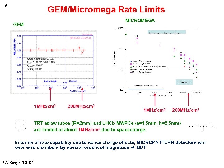 6 GEM/Micromega Rate Limits MICROMEGA GEM 1 MHz/cm 2 200 MHz/cm 2 TRT straw tubes (R=2 mm) and LHCb MWPCs (s=1. 5 mm, h=2. 5 mm) are limited at about 1 MHz/cm 2 due to spacecharge. In terms of rate capability due to space charge effects, MICROPATTERN detectors win over wire chambers by several orders of magnitude BUT W. Riegler/CERN
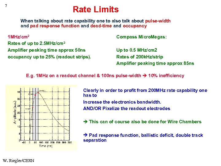 7 Rate Limits When talking about rate capability one to also talk about pulse-width and pad response function and dead-time and occupancy 1 MHz/cm 2 Rates of up to 2. 5 MHz/cm 2 Amplifier peaking time approx 50 ns occupancy up to 25% (readout strips). Compass Micro. Megas: Up to 0. 5 MHz/cm 2 Rates of 200 k. Hz/strip Amplifier peaking time approx 85 ns E. g. 1 MHz on a readout channel & 100 ns pulse-width 10% inefficiency Clearly in order to profit from 200 MHz rate capability one has to Increase the electronics bandwidth. AND/OR Pixelize the readout electrodes This can of course also be done for Wire Chambers Pad response function, ballistic deficit, double track separation W. Riegler/CERN
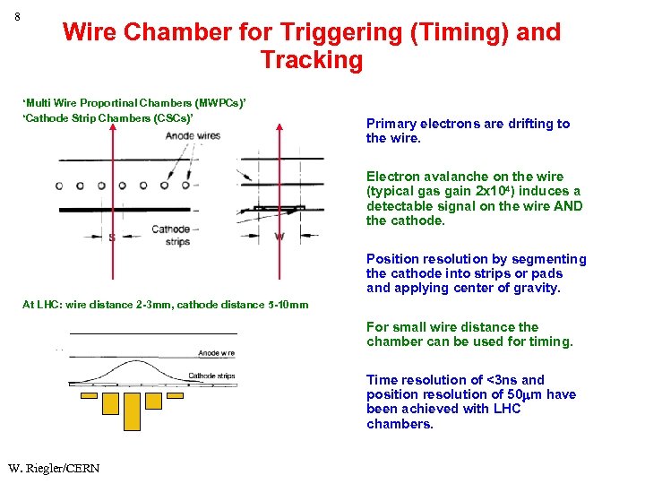 8 Wire Chamber for Triggering (Timing) and Tracking ‘Multi Wire Proportinal Chambers (MWPCs)’ ‘Cathode Strip Chambers (CSCs)’ Primary electrons are drifting to the wire. Electron avalanche on the wire (typical gas gain 2 x 10⁴) induces a detectable signal on the wire AND the cathode. Position resolution by segmenting the cathode into strips or pads and applying center of gravity. At LHC: wire distance 2 -3 mm, cathode distance 5 -10 mm For small wire distance the chamber can be used for timing. Time resolution of <3 ns and position resolution of 50 m have been achieved with LHC chambers. W. Riegler/CERN
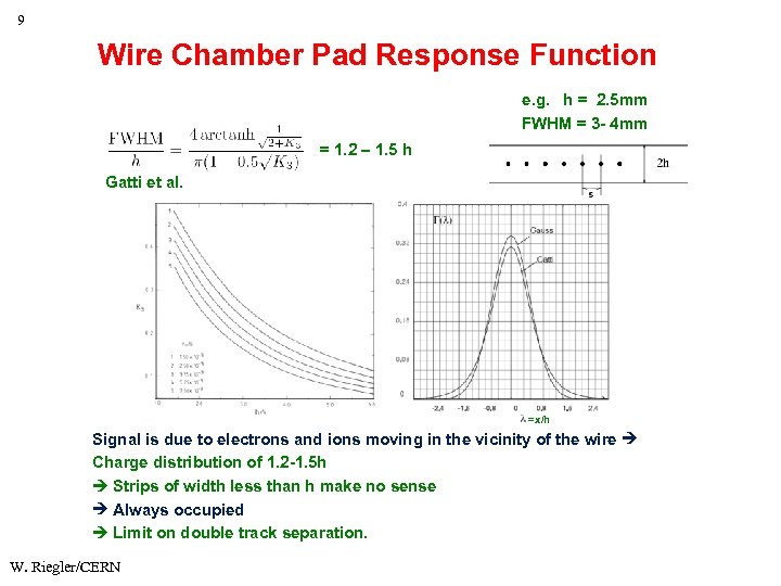 9 Wire Chamber Pad Response Function e. g. h = 2. 5 mm FWHM = 3 - 4 mm = 1. 2 – 1. 5 h Gatti et al. =x/h Signal is due to electrons and ions moving in the vicinity of the wire Charge distribution of 1. 2 -1. 5 h Strips of width less than h make no sense Always occupied Limit on double track separation. W. Riegler/CERN
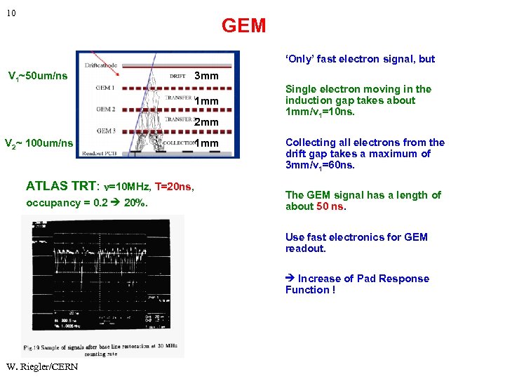 10 GEM ‘Only’ fast electron signal, but V 1~50 um/ns 3 mm 1 mm 2 mm V 2~ 100 um/ns ATLAS TRT: =10 MHz, T=20 ns, occupancy = 0. 2 20%. 1 mm Single electron moving in the induction gap takes about 1 mm/v 1=10 ns. Collecting all electrons from the drift gap takes a maximum of 3 mm/v 1=60 ns. The GEM signal has a length of about 50 ns. Use fast electronics for GEM readout. Increase of Pad Response Function ! W. Riegler/CERN
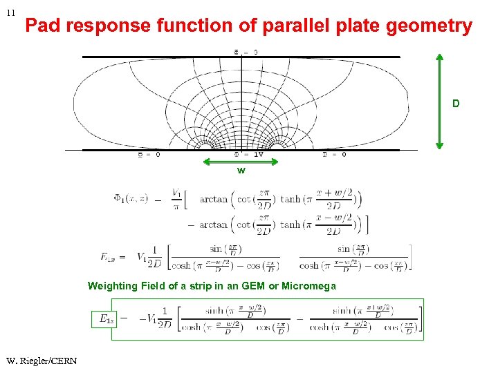 11 Pad response function of parallel plate geometry D w Weighting Field of a strip in an GEM or Micromega W. Riegler/CERN
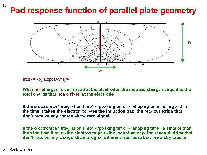 12 Pad response function of parallel plate geometry v D w I(t, x) = -e 0*Ez[x, D-v*t]*v When all charges have arrived at the electrodes the induced charge is equal to the total charge that has arrived at the electrode. If the electronics ‘integration time’ ~ ‘peaking time’ ~ ‘shaping time’ is larger than the time it takes the electron to pass the induction gap, the readout strips that don’t receive any charge show zero signal. If the electronics ‘integration time’ ~ ‘peaking time’ ~ ‘shaping time’ is smaller than the time it takes the electron to pass the induction gap, the readout strips that don’t receive any charge show a signal different from zero that is strictly bipolar. W. Riegler/CERN
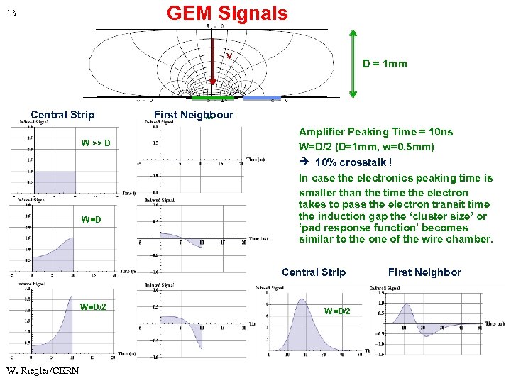 GEM Signals 13 v Central Strip W >> D W=D D = 1 mm First Neighbour w Amplifier Peaking Time = 10 ns W=D/2 (D=1 mm, w=0. 5 mm) 10% crosstalk ! In case the electronics peaking time is smaller than the time the electron takes to pass the electron transit time the induction gap the ‘cluster size’ or ‘pad response function’ becomes similar to the one of the wire chamber. Central Strip W=D/2 W. Riegler/CERN W=D/2 First Neighbor
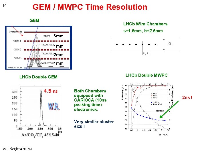 GEM / MWPC Time Resolution 14 GEM LHCb Wire Chambers s=1. 5 mm, h=2. 5 mm 3 mm 1 mm 2 mm 1 mm LHCb Double MWPC LHCb Double GEM Both Chambers equipped with CARIOCA (10 ns peaking time) electronics. Very similar cluster size ! W. Riegler/CERN 2 ns !
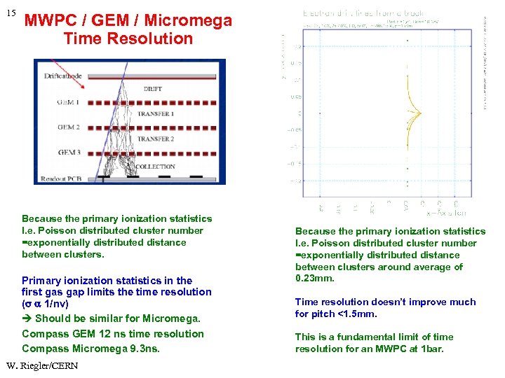 15 MWPC / GEM / Micromega Time Resolution Because the primary ionization statistics I. e. Poisson distributed cluster number =exponentially distributed distance between clusters. Primary ionization statistics in the first gas gap limits the time resolution ( 1/nv) Should be similar for Micromega. Compass GEM 12 ns time resolution Compass Micromega 9. 3 ns. W. Riegler/CERN Because the primary ionization statistics I. e. Poisson distributed cluster number =exponentially distributed distance between clusters around average of 0. 23 mm. Time resolution doesn’t improve much for pitch <1. 5 mm. This is a fundamental limit of time resolution for an MWPC at 1 bar.
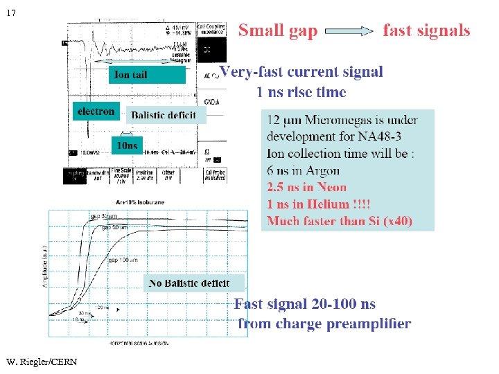
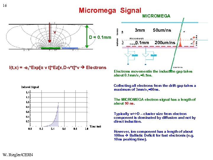 16 Micromega Signal MICROMEGA 3 mm v 50 um/ns D = 0. 1 mm I(t, x) = -e 0*Exp[α v t]*Ez[x, D-v*t]*v Electrons 200 um/ns Electrons movementin the induction gap takes about 0. 1 mm/v 1=0. 5 ns. Collecting all electrons from the drift gap takes a maximum of 3 mm/v 1=60 ns. The MICROMEGA electron signal has a length of about 50 ns. Typically w>>D – cluster size from electron component is dominated by diffusion and not by direct induction. However, ion component has a length of about 100 ns Ballistic Deficit for fast electronis (e. g. 10 ns peaking time). W. Riegler/CERN
 17 W. Riegler/CERN
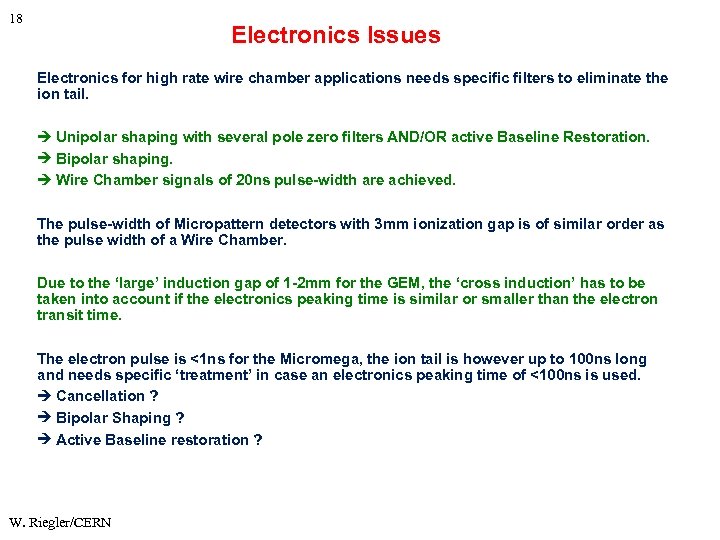 18 Electronics Issues Electronics for high rate wire chamber applications needs specific filters to eliminate the ion tail. Unipolar shaping with several pole zero filters AND/OR active Baseline Restoration. Bipolar shaping. Wire Chamber signals of 20 ns pulse-width are achieved. The pulse-width of Micropattern detectors with 3 mm ionization gap is of similar order as the pulse width of a Wire Chamber. Due to the ‘large’ induction gap of 1 -2 mm for the GEM, the ‘cross induction’ has to be taken into account if the electronics peaking time is similar or smaller than the electron transit time. The electron pulse is <1 ns for the Micromega, the ion tail is however up to 100 ns long and needs specific ‘treatment’ in case an electronics peaking time of <100 ns is used. Cancellation ? Bipolar Shaping ? Active Baseline restoration ? W. Riegler/CERN
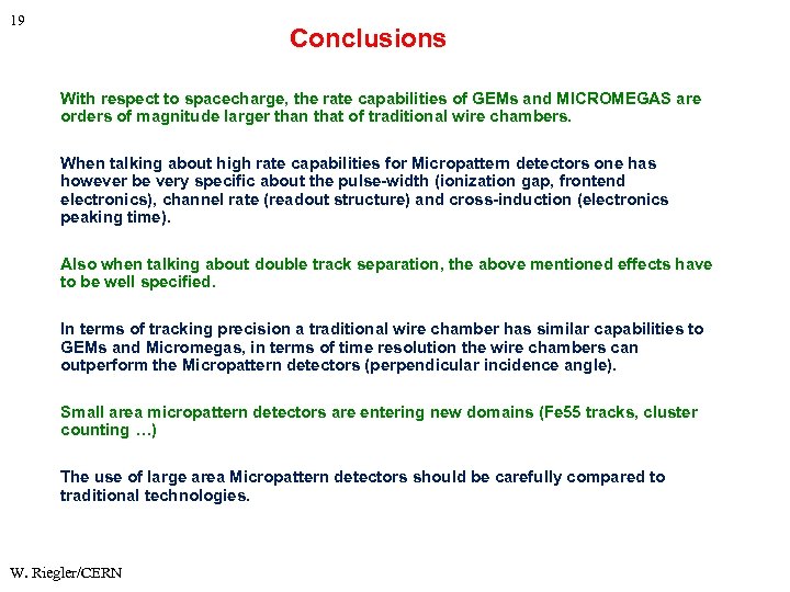 19 Conclusions With respect to spacecharge, the rate capabilities of GEMs and MICROMEGAS are orders of magnitude larger than that of traditional wire chambers. When talking about high rate capabilities for Micropattern detectors one has however be very specific about the pulse-width (ionization gap, frontend electronics), channel rate (readout structure) and cross-induction (electronics peaking time). Also when talking about double track separation, the above mentioned effects have to be well specified. In terms of tracking precision a traditional wire chamber has similar capabilities to GEMs and Micromegas, in terms of time resolution the wire chambers can outperform the Micropattern detectors (perpendicular incidence angle). Small area micropattern detectors are entering new domains (Fe 55 tracks, cluster counting …) The use of large area Micropattern detectors should be carefully compared to traditional technologies. W. Riegler/CERN


