1 BJT Bipolar Junction Transistor


- Размер: 3.9 Mегабайта
- Количество слайдов: 100
Описание презентации 1 BJT Bipolar Junction Transistor по слайдам
 1 BJT Bipolar Junction Transistor • Widely used in amplifier circuits • Formed by junction of 3 materials • npn or pnp structure
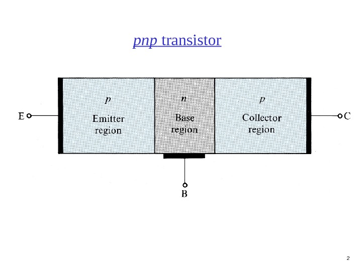
 2 pnp transistor
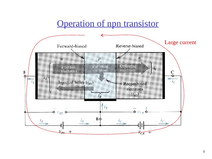
 3 Large current. Operation of npn transistor
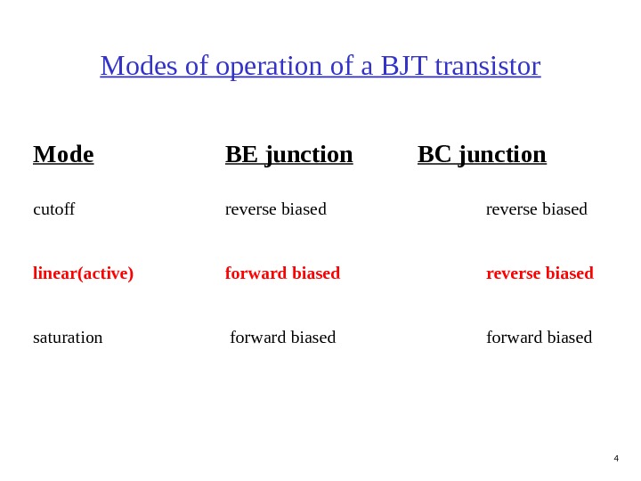
 4 Modes of operation of a BJT transistor Mode BE junction BC junction cutoff reverse biased linear(active) forward biased reverse biased saturation forward biased
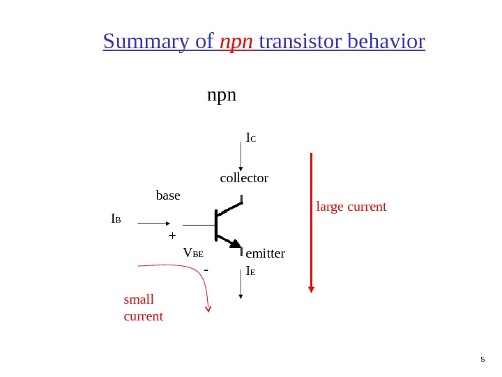
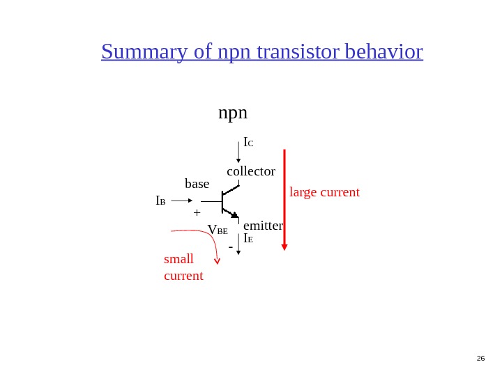
 5 Summary of npn transistor behavior npn collector emitterbase I B I EI C small current large current + V BE —
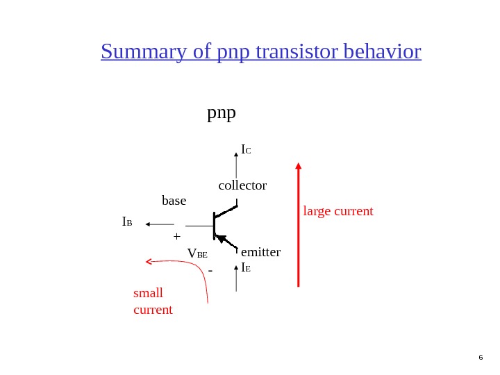
 6 Summary of pnp transistor behavior pnp collector emitterbase I B I EI C small current large current + V BE —
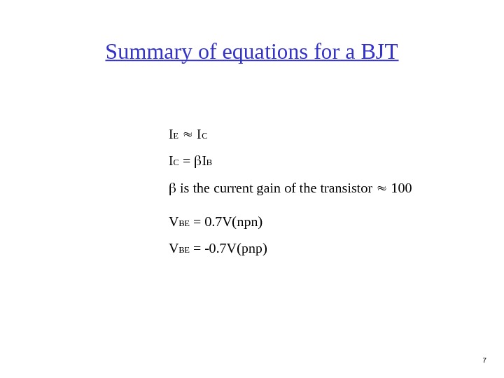
 7 Summary of equations for a BJT I E I C = I B is the current gain of the transistor 100 V BE = 0. 7 V(npn) V BE = -0. 7 V(pnp)
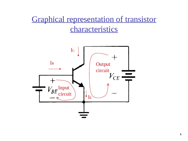
 8 Graphical representation of transistor characteristics I B I C I E Output circuit Input circuit
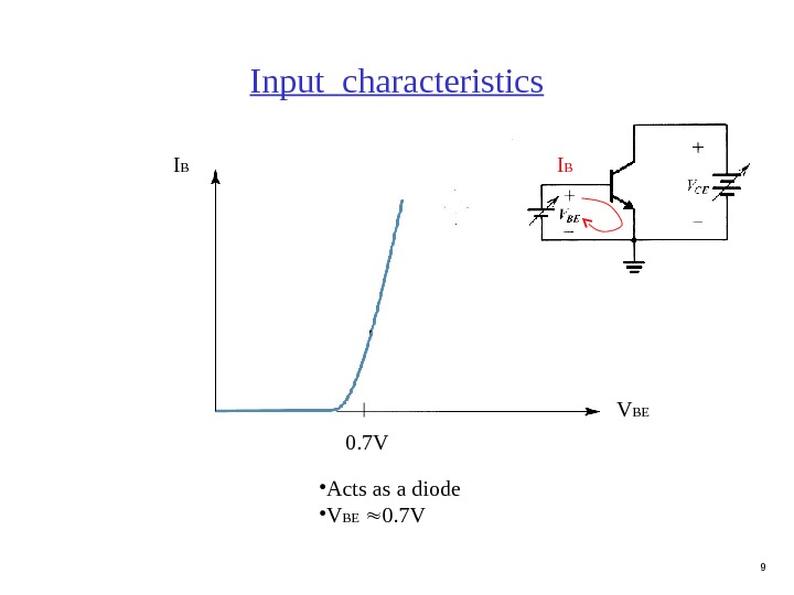
 9 Input characteristics • Acts as a diode • V BE 0. 7 VI B V BE 0. 7 V
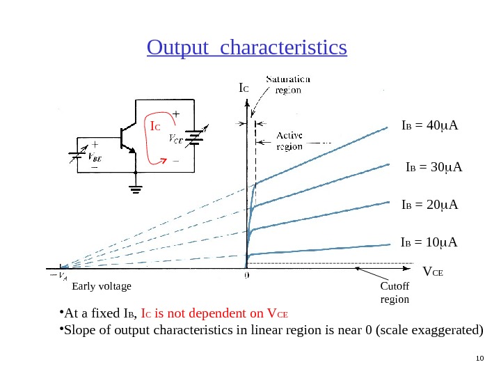
 10 Output characteristics I C V CEI B = 10 AI B = 20 AI B = 30 AI B = 40 A Cutoff region • At a fixed I B , I C is not dependent on V CE • Slope of output characteristics in linear region is near 0 (scale exaggerated) Early voltage
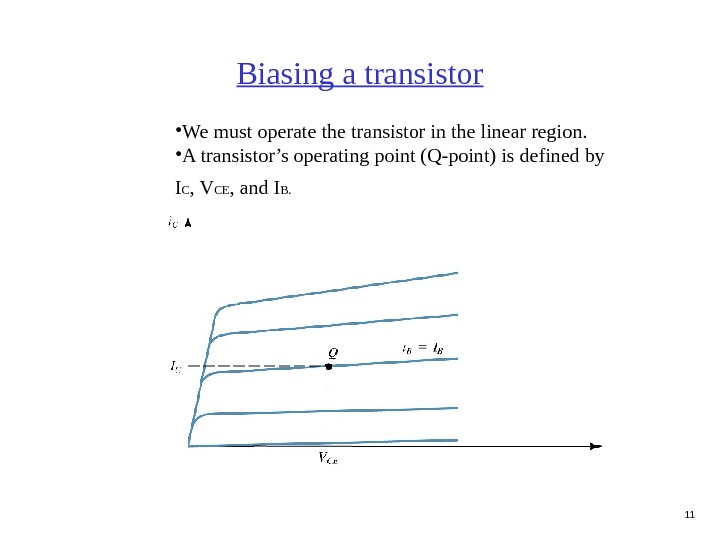
 11 Biasing a transistor • We must operate the transistor in the linear region. • A transistor’s operating point (Q-point) is defined by I C , V CE , and I B.
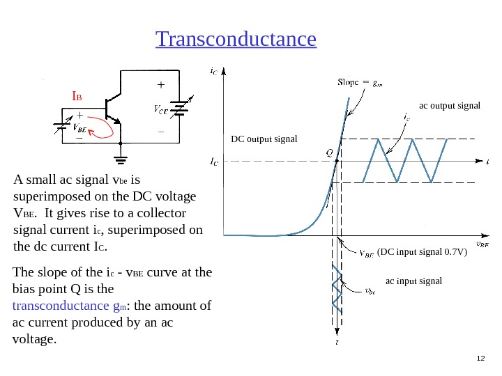
 12 A small ac signal v be is superimposed on the DC voltage V BE. It gives rise to a collector signal current i c , superimposed on the dc current I C. Transconductance ac input signal(DC input signal 0. 7 V) ac output signal DC output signal. I B The slope of the i c — v BE curve at the bias point Q is the transconductance g m : the amount of ac current produced by an ac voltage.
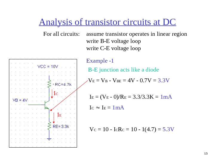
 13 Analysis of transistor circuits at DC For all circuits: assume transistor operates in linear region write B-E voltage loop write C-E voltage loop Example -1 B-E junction acts like a diode V E = V B — V BE = 4 V — 0. 7 V = 3. 3 V I EI C I E = (V E — 0)/R E = 3. 3/3. 3 K = 1 m. A I C I E = 1 m. A V C = 10 — I C R C = 10 — 1(4. 7) = 5. 3 V
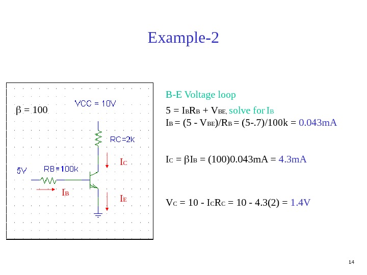
 14 Example-2 B-E Voltage loop 5 = I B R B + V BE, solve for I B = (5 — V BE )/R B = (5 -. 7)/100 k = 0. 043 m. A I C = I B = (100)0. 043 m. A = 4. 3 m. A V C = 10 — I C R C = 10 — 4. 3(2) = 1. 4 VI EI C I B =
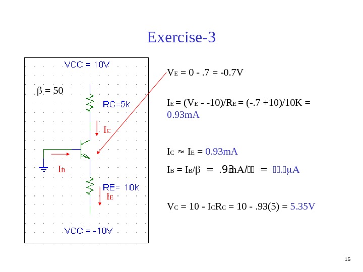
 15 Exercise-3 V E = 0 -. 7 = -0. 7 V I EI C I B = 50 I E = (V E — -10)/R E = (-. 7 +10)/10 K = 0. 93 m. A I C I E = 0. 93 m. A I B = I B / m V C = 10 — I C R C = 10 -. 93(5) = 5. 35 V
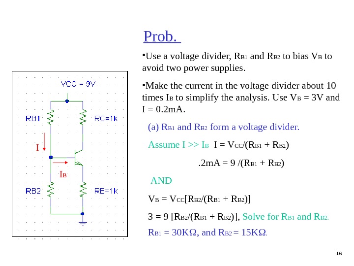
 16 Prob. • Use a voltage divider, R B 1 and R B 2 to bias V B to avoid two power supplies. • Make the current in the voltage divider about 10 times I B to simplify the analysis. Use V B = 3 V and I = 0. 2 m. A. I BI (a) R B 1 and R B 2 form a voltage divider. Assume I >> I B I = V CC /(R B 1 + R B 2 ) . 2 m. A = 9 /(R B 1 + R B 2 ) AND V B = V CC [R B 2 /(R B 1 + R B 2 )] 3 = 9 [R B 2 /(R B 1 + R B 2 )], Solve for R B 1 and R B 2. R B 1 = 30 K , and R B 2 = 15 K .
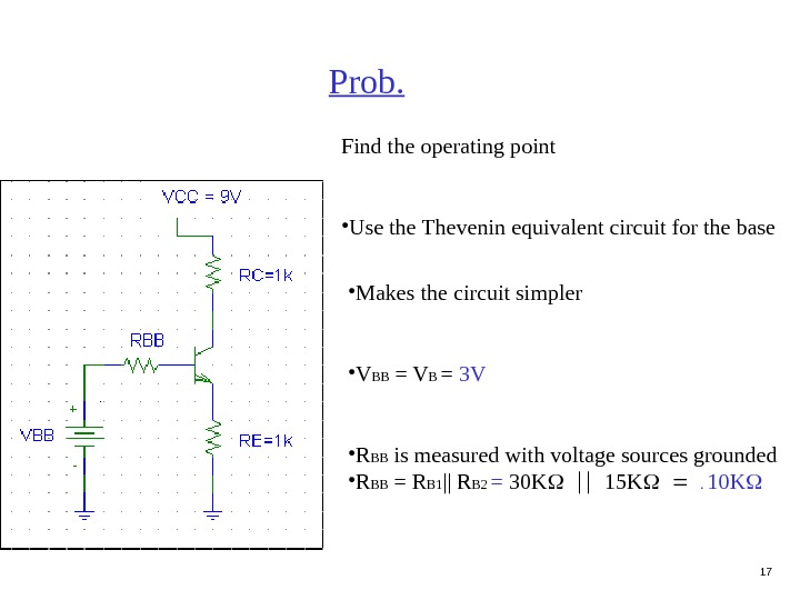
 17 Prob. Find the operating point • Use the Thevenin equivalent circuit for the base • Makes the circuit simpler • V BB = V B = 3 V • R BB is measured with voltage sources grounded • R BB = R B 1 || R B 2 = 30 K 15 K . 10 K
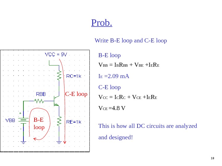
 18 Prob. Write B-E loop and C-E loop B-E loop V BB = I B R BB + V BE +I E R E I E =2. 09 m. A C-E loop V CC = I C R C + V CE +I E R E V CE =4. 8 V This is how all DC circuits are analyzed and designed!
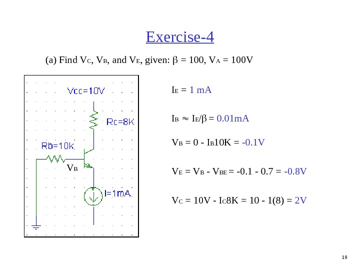
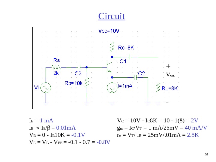
 19 Exercise-4 (a) Find V C , V B , and V E , given: = 100, V A = 100 V I E = 1 m. A I B I E / = 0. 01 m. A V B = 0 — I B 10 K = -0. 1 V V E = V B — V BE = -0. 1 — 0. 7 = -0. 8 V V C = 10 V — I C 8 K = 10 — 1(8) = 2 VV
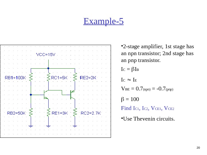
 20 Example-5 • 2 -stage amplifier, 1 st stage has an npn transistor; 2 nd stage has an pnp transistor. I C = I B I C I E V BE = 0. 7 (npn) = -0. 7 (pnp) = 100 Find I C 1 , I C 2 , V CE 1 , V CE 2 • Use Thevenin circuits.
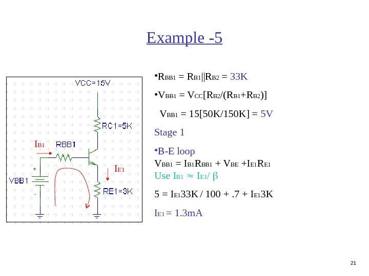
 21 Example -5 • R BB 1 = R B 1 ||R B 2 = 33 K • V BB 1 = V CC [R B 2 /(R B 1 +R B 2 )] V BB 1 = 15[50 K/150 K] = 5 V Stage 1 • B-E loop V BB 1 = I B 1 R BB 1 + V BE +I E 1 R E 1 Use I B 1 I E 1 / 5 = I E 1 33 K / 100 +. 7 + I E 1 3 K I E 1 = 1. 3 m. AI B 1 I
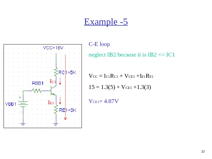
 22 Example -5 C-E loop neglect IB 2 because it is IB 2 << IC 1 I E 1 I C 1 V CC = I C 1 R C 1 + V CE 1 +I E 1 R E 1 15 = 1. 3(5) + V CE 1 +1. 3(3) V CE 1 = 4. 87 V
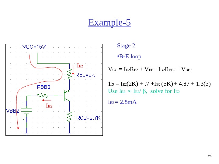
 23 Example-5 Stage 2 • B-E loop I B 2 I E 2 V CC = I E 2 R E 2 + V EB +I B 2 R BB 2 + V BB 2 15 = I E 2 (2 K) +. 7 +I B 2 (5 K) + 4. 87 + 1. 3(3) Use I B 2 I E 2 / solve for I E 2 = 2. 8 m.
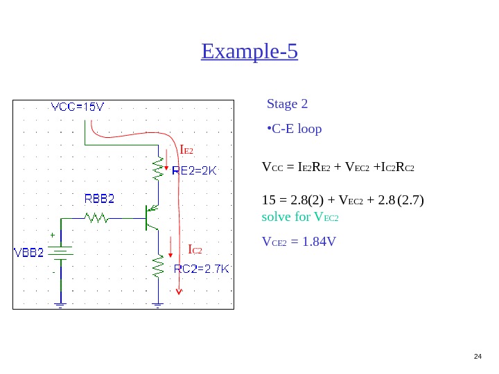
 24 Example-5 Stage 2 • C-E loop I E 2 I C 2 V CC = I E 2 R E 2 + V EC 2 +I C 2 R C 2 15 = 2. 8(2) + V EC 2 + 2. 8 (2. 7) solve for V EC 2 V CE 2 = 1. 84 V
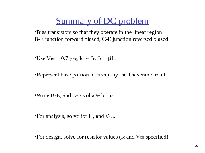
 25 Summary of DC problem • Bias transistors so that they operate in the linear region B-E junction forward biased, C-E junction reversed biased • Use V BE = 0. 7 (npn), I C I E , I C = I B • Represent base portion of circuit by the Thevenin circuit • Write B-E, and C-E voltage loops. • For analysis, solve for I C , and V CE. • For design, solve for resistor values (I C and V CE specified).
 26 Summary of npn transistor behavior npn collector emitterbase I B I EI C small current large current + V BE —
 27 Transistor as an amplifier • Transistor circuits are analyzed and designed in terms of DC and ac versions of the same circuit. • An ac signal is usually superimposed on the DC circuit. • The location of the operating point (values of I C and V CE ) of the transistor affects the ac operation of the circuit. • There at least two ac parameters determined from DC quantities.
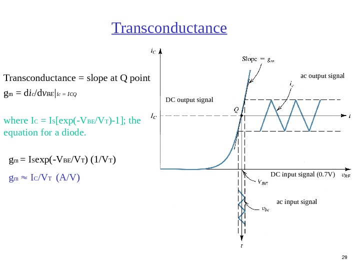
 28 A small ac signal v be is superimposed on the DC voltage V BE. It gives rise to a collector signal current i c , superimposed on the dc current I C. Transconductance ac input signal(DC input signal 0. 7 V) ac output signal DC output signal. I B The slope of the i c — v BE curve at the bias point Q is the transconductance g m : the amount of ac current produced by an ac voltage.
 29 Transconductance = slope at Q point g m = d i c /d v BE | i c = I CQ where I C = I S [exp(-V BE /V T )-1]; the equation for a diode. Transconductance ac input signal. DC input signal (0. 7 V) ac output signal DC output signal g m = I S exp(-V BE /V T ) (1/V T ) g m I C /V T (A/V)
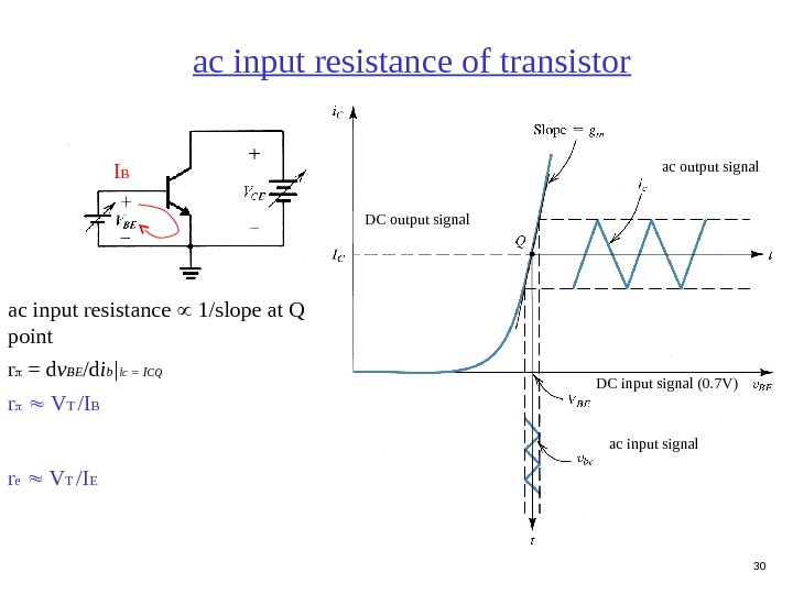
 30 ac input resistance 1/slope at Q point r = d v BE /d i b | i c = I CQ r V T /I B r e V T /I E ac input resistance of transistor ac input signal. DC input signal (0. 7 V) ac output signal DC output signal. I
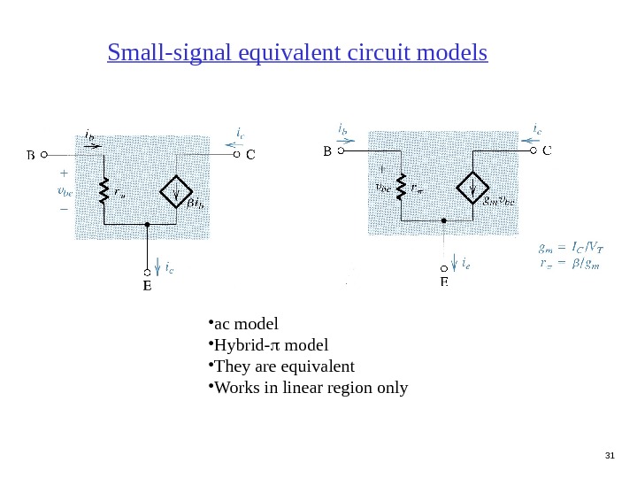
 31 Small-signal equivalent circuit models • ac model • Hybrid- model • They are equivalent • Works in linear region only
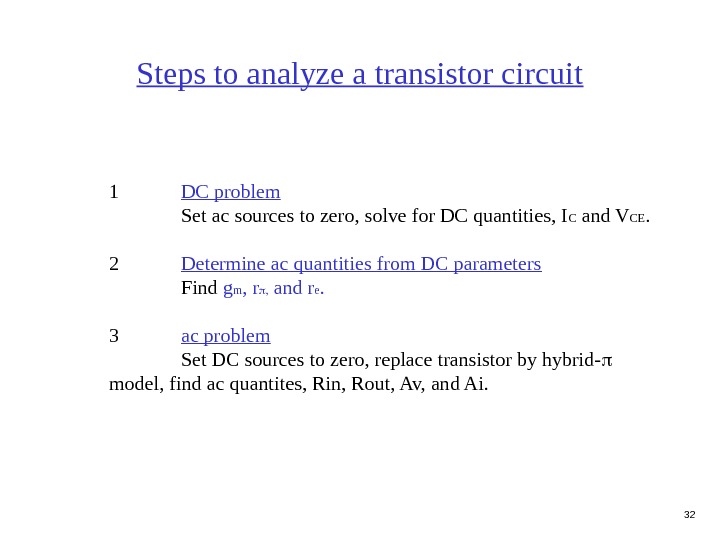
 32 Steps to analyze a transistor circuit 1 DC problem Set ac sources to zero, solve for DC quantities, I C and V CE. 2 Determine ac quantities from DC parameters Find g m , r and r e. 3 ac problem Set DC sources to zero, replace transistor by hybrid- model, find ac quantites, Rin, Rout, Av, and Ai.
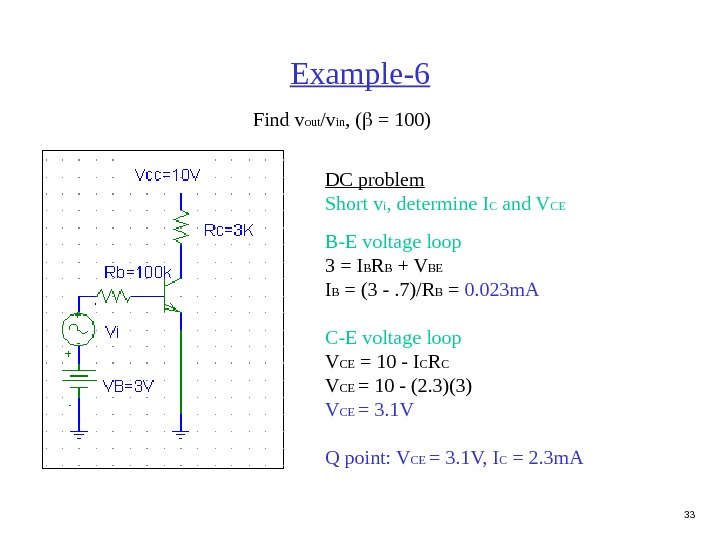
 33 Example-6 Find v out /v in , ( = 100) DC problem Short v i , determine I C and V CE B-E voltage loop 3 = I B R B + V BE I B = (3 -. 7)/R B = 0. 023 m. A C-E voltage loop V CE = 10 — I C R C V CE = 10 — (2. 3)(3) V CE = 3. 1 V Q point: V CE = 3. 1 V, I C = 2. 3 m.
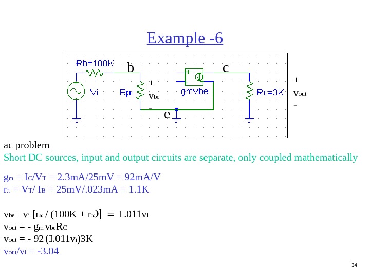
 34 Example -6 ac problem Short DC sources, input and output circuits are separate, only coupled mathematically g m = I C /V T = 2. 3 m. A/25 m. V = 92 m. A/V r = V T / I B = 25 m. V/. 023 m. A = 1. 1 K v be = v i [ r / (100 K + r 011 v i v out = — g m v be R C v out = — 92 ( 011 v i ) 3 K v out /v i = -3. 04 + v out — eb c + v be —
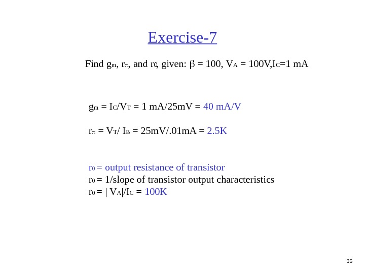
 35 Exercise-7 Find g m , r , and r , given: = 100, V A = 100 V, I C =1 m. A g m = I C /V T = 1 m. A/25 m. V = 40 m. A/V r = V T / I B = 25 m. V/. 01 m. A = 2. 5 K r 0 = output resistance of transistor r 0 = 1/slope of transistor output characteristics r 0 = | V A |/I C = 100 K
 36 Summary of transistor analysis • Transistor circuits are analyzed and designed in terms of DC and ac versions of the same circuit. • An ac signal is usually superimposed on the DC circuit. • The location of the operating point (values of I C and V CE ) of the transistor affects the ac operation of the circuit. • There at least two ac parameters determined from DC quantities.
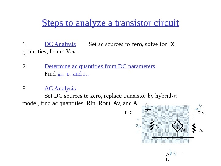
 37 Steps to analyze a transistor circuit 1 DC Analysis Set ac sources to zero, solve for DC quantities, I C and V CE. 2 Determine ac quantities from DC parameters Find g m , r and r o. 3 AC Analysis Set DC sources to zero, replace transistor by hybrid- model, find ac quantities, Rin, Rout, Av, and Ai. r o
 38 Circuit I E = 1 m. A V C = 10 V — I C 8 K = 10 — 1(8) = 2 V I B I E / = 0. 01 m. A g m = I C /V T = 1 m. A/25 m. V = 40 m. A/V V B = 0 — I B 10 K = -0. 1 V r = V T / I B = 25 m. V/. 01 m. A = 2. 5 K V E = V B — V BE = -0. 1 — 0. 7 = -0. 8 V + V out —
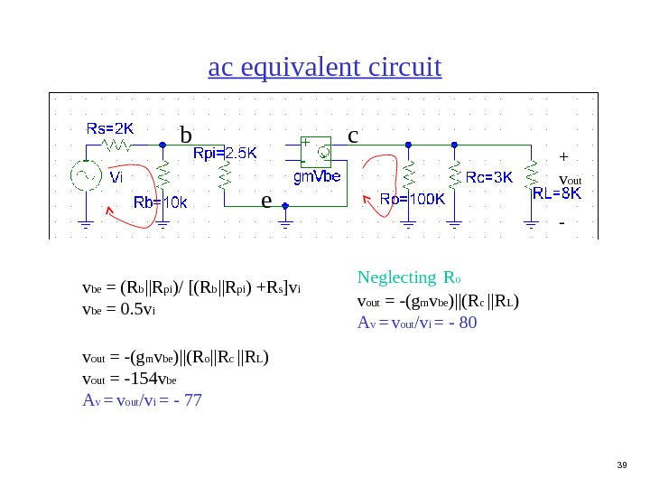
 39 ac equivalent circuit b e c v be = (R b ||R pi )/ [(R b ||R pi ) +R s ]v i v be = 0. 5 v i v out = -(g m v be )||(R o ||R c ||R L ) v out = -154 v be A v = v out /v i = — 77 + v out — Neglecting R o v out = -(g m v be )||(R c ||R L ) A v = v out /v i = —
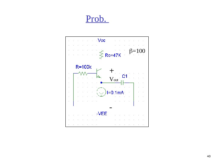
 40 Prob. + V out — =
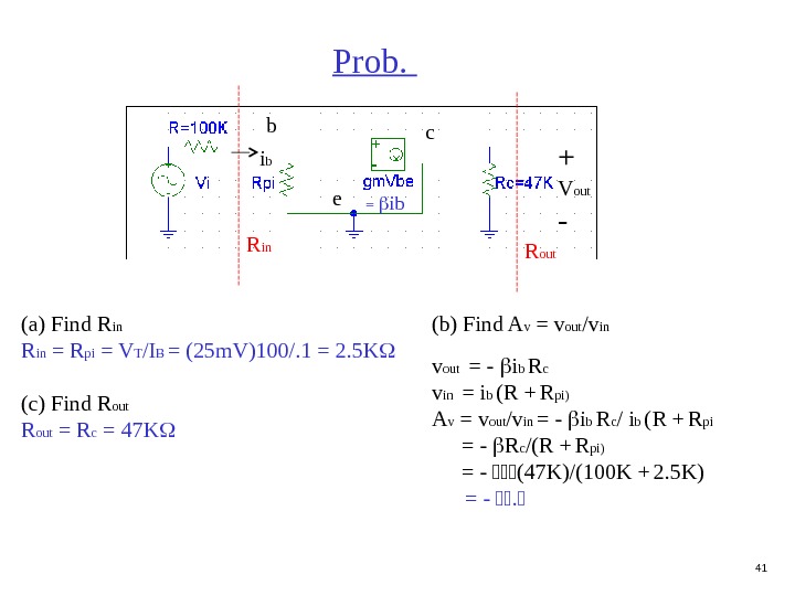
 41 Prob. + V out — (a) Find R in = R pi = V T /I B = (25 m. V)100/. 1 = 2. 5 K (c) Find R out = R c = 47 K R in R out (b) Find A v = v out /v in v out = — i b R c v in = i b (R + R pi) A v = v out /v in = — i b R c / i b (R + R pi = — R c /(R + R pi) = — (47 K)/(100 K + 2. 5 K) = — = ibb e c i b
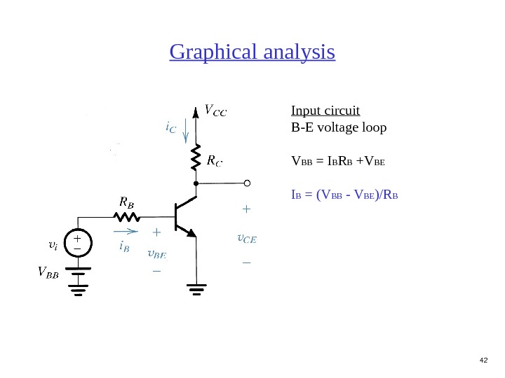
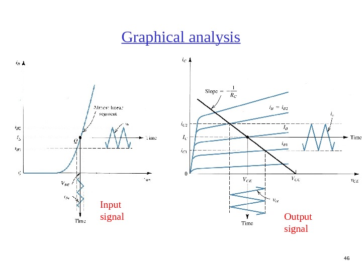
 42 Graphical analysis Input circuit B-E voltage loop V BB = I B R B +V BE I B = (V BB — V BE )/R
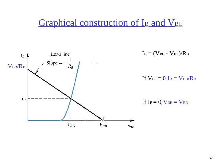
 43 Graphical construction of I B and V BE I B = (V BB — V BE )/R B If V BE = 0 , I B = V BB /R B If I B = 0 , V BE = V BB /R
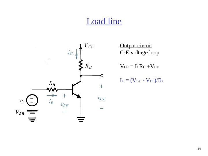
 44 Load line Output circuit C-E voltage loop V CC = I C R C +V CE I C = (V CC — V CE )/R
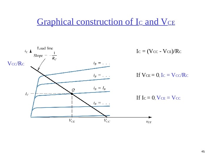
 45 Graphical construction of I C and V CE V CC /R C I C = (V CC — V CE )/R C If V CE = 0 , I C = V CC /R C If I C = 0 , V CE = V
 46 Graphical analysis Input signal Output signal
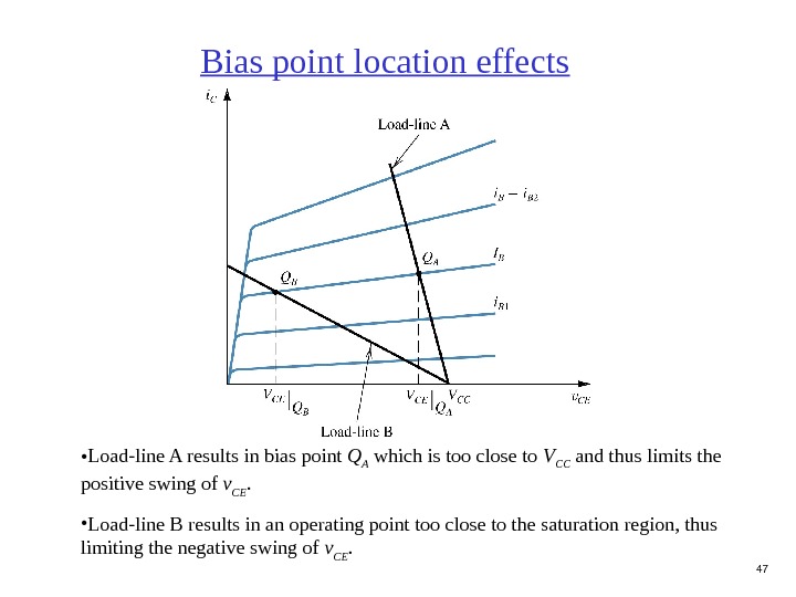
 47 • Load-line A results in bias point Q A which is too close to V CC and thus limits the positive swing of v CE. • Load-line B results in an operating point too close to the saturation region, thus limiting the negative swing of v CE. Bias point location effects
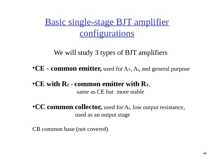
 48 Basic single-stage BJT amplifier configurations We will study 3 types of BJT amplifiers • CE — common emitter, used for A V , A i , and general purpose • CE with R E — common emitter with R E , same as CE but more stable • CC common collector, used for A i , low output resistance, used as an output stage CB common base (not covered)
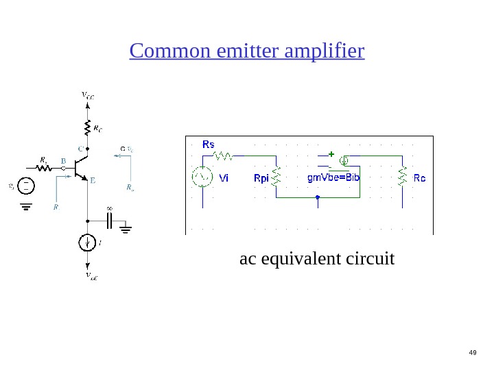
 49 Common emitter amplifier ac equivalent circuit
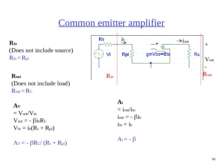
 50 Common emitter amplifier R in R out+ V out -R in (Does not include source) R in = R pi R out (Does not include load) R out = R C A V = V out /V in V out = — i b R C V in = i b (R s + R pi ) A V = — R C / (R s + R pi ) A i = i out /i in i out = — i b i in = i b A i = — i b i out
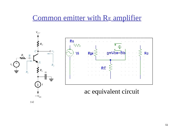
 51 Common emitter with R E amplifier ac equivalent circuit
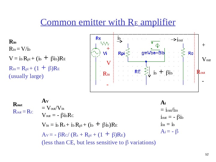
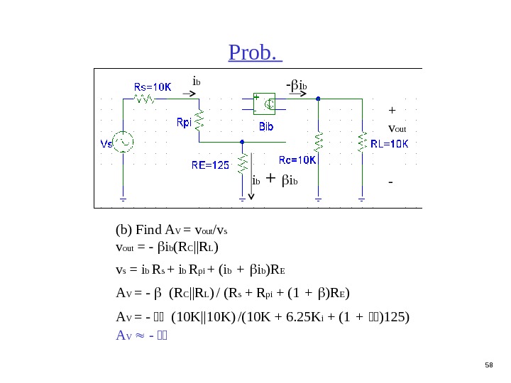
 52 Common emitter with R E amplifier R in R out + V out -R in = V/i b V = i b R pi + (i b + i b )R E R in = R pi + (1 + )R E (usually large) R out = R C A V = V out /V in V out = — i b R C V in = i b R s + i b R pi + (i b + i b )R E A V = — R C / (R s + R pi + (1 + )R E ) (less than CE, but less sensitive to variations) A i = i out /i in i out = — i b i in = i b A i = — i b i out i b + i b+ V —
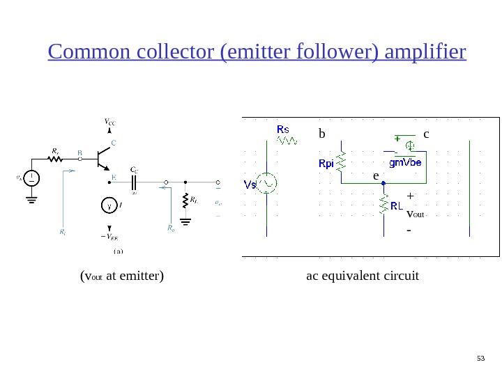
 53 Common collector (emitter follower) amplifier b c e + v out — (v out at emitter) ac equivalent circuit
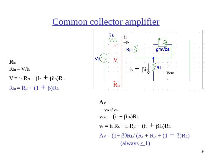
 54 Common collector amplifier R in + v out -R in = V/i b V = i b R pi + (i b + i b )R L R in = R pi + (1 + )R L A V = v out /v s v out = (i b + i b )R L v s = i b R s + i b R pi + (i b + i b )R L A V = (1+ R L / (R s + R pi + (1 + )R L ) (always < 1)i b + i b+ V —
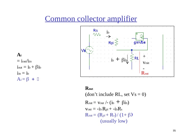
 55 Common collector amplifier R out+ v out — R out (don’t include RL, set Vs = 0) R out = v out /- ( i b + i b ) v out = -i b R pi + -i b R s R out = (R pi + R s ) / (1+ (usually low)A i = i out /i in i out = i b + i b i in = i b A i = i b + i b
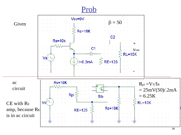
 56 Prob + v out — = 50 ac circuit CE with R E amp, because R E is in ac circuit Given R pi =V T /I B = 25 m. V(50)/. 2 m. A = 6. 25 K
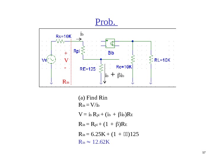
 57 Prob. (a) Find Rin R in = V/i b V = i b R pi + (i b + i b )R E R in = R pi + (1 + )R E R in = 6. 25 K + (1 + )125 R in 12. 62 KR in+ V — i b + i b
 58 Prob. (b) Find A V = v out /v s v out = — i b (R C ||R L ) v s = i b R s + i b R pi + (i b + i b )R E A V = — (R C ||R L ) / (R s + R pi + (1 + )R E ) A V = — (10 K||10 K) /(10 K + 6. 25 K i + (1 + )125) A V — i b + v out — i b
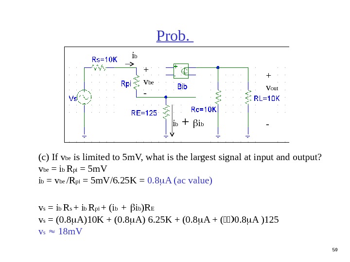
 59 Prob. (c) If v be is limited to 5 m. V, what is the largest signal at input and output? v be = i b R pi = 5 m. V i b = v be / R pi = 5 m. V/6. 25 K = 0. 8 A (ac value) v s = i b R s + i b R pi + (i b + i b )R E v s = (0. 8 A)10 K + (0. 8 A) 6. 25 K + (0. 8 A + ( 0. 8 A )125 v s 18 m. V i b + v out -+ v be —
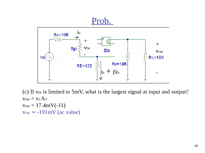
 60 Prob. (c) If v be is limited to 5 m. V, what is the largest signal at input and output? v out = v s A V v out = 17. 4 m. V(-11) v out -191 m. V (ac value) i b + v out -+ v be —
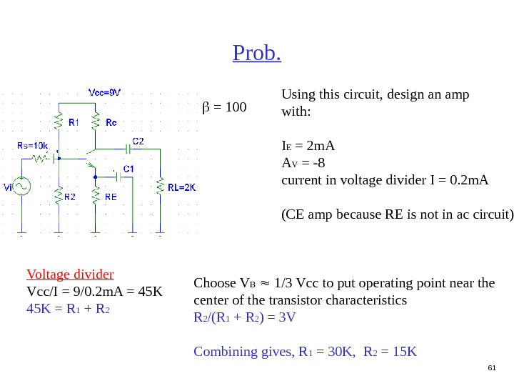
 61 Prob. Using this circuit, design an amp with: I E = 2 m. A A V = -8 current in voltage divider I = 0. 2 m. A (CE amp because RE is not in ac circuit) = 100 Voltage divider Vcc/I = 9/0. 2 m. A = 45 K = R 1 + R 2 Choose V B 1/3 Vcc to put operating point near the center of the transistor characteristics R 2 /(R 1 + R 2 ) = 3 V Combining gives, R 1 = 30 K, R 2 = 15 K
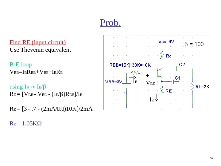
 62 Prob. = 100 Find RE (input circuit) Use Thevenin equivalent B-E loop V BB =I B R BB +V BE +I E R E using I B I E / R E = [V BB — V BE — (I E / )R BB ]/I E R E = [3 -. 7 — (2 m. A/ )10 K]/2 m. A R E = 1. 05 K + V BE — I EI
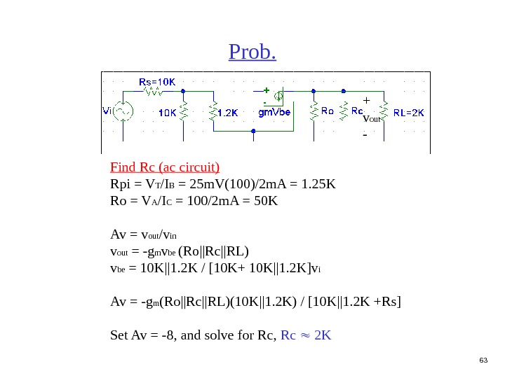
 63 Prob. Find Rc (ac circuit) Rpi = V T /I B = 25 m. V(100)/2 m. A = 1. 25 K Ro = V A /I C = 100/2 m. A = 50 K Av = v out /v in v out = -g m v be (Ro||Rc||RL) v be = 10 K||1. 2 K / [10 K+ 10 K||1. 2 K]v i Av = -g m (Ro||Rc||RL)(10 K||1. 2 K) / [10 K||1. 2 K +Rs] Set Av = -8, and solve for Rc, Rc 2 K + v out —
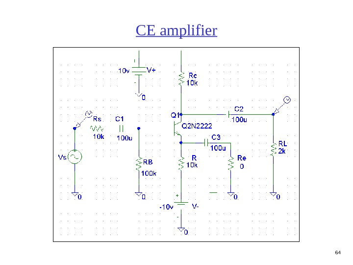
 64 CE amplifier
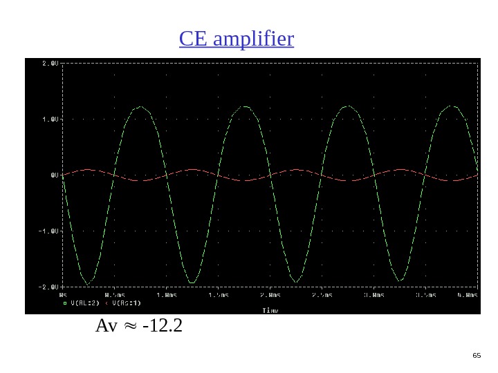
 65 CE amplifier Av -12.
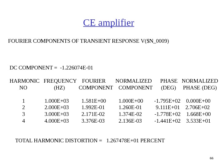
 66 FOURIER COMPONENTS OF TRANSIENT RESPONSE V($N_0009) DC COMPONENT = -1. 226074 E-01 HARMONIC FREQUENCY FOURIER NORMALIZED PHASE NORMALIZED NO (HZ) COMPONENT (DEG) PHASE (DEG) 1 1. 000 E+03 1. 581 E+00 1. 000 E+00 -1. 795 E+02 0. 000 E+00 2 2. 000 E+03 1. 992 E-01 1. 260 E-01 9. 111 E+01 2. 706 E+02 3 3. 000 E+03 2. 171 E-02 1. 374 E-02 -1. 778 E+02 1. 668 E+00 4 4. 000 E+03 3. 376 E-03 2. 136 E-03 -1. 441 E+02 3. 533 E+01 TOTAL HARMONIC DISTORTION = 1. 267478 E+01 PERCENT CE amplifier
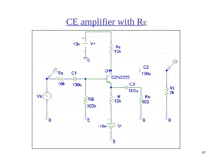
 67 CE amplifier with R
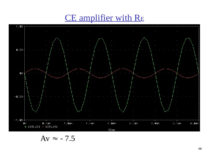
 68 CE amplifier with R E Av — 7.
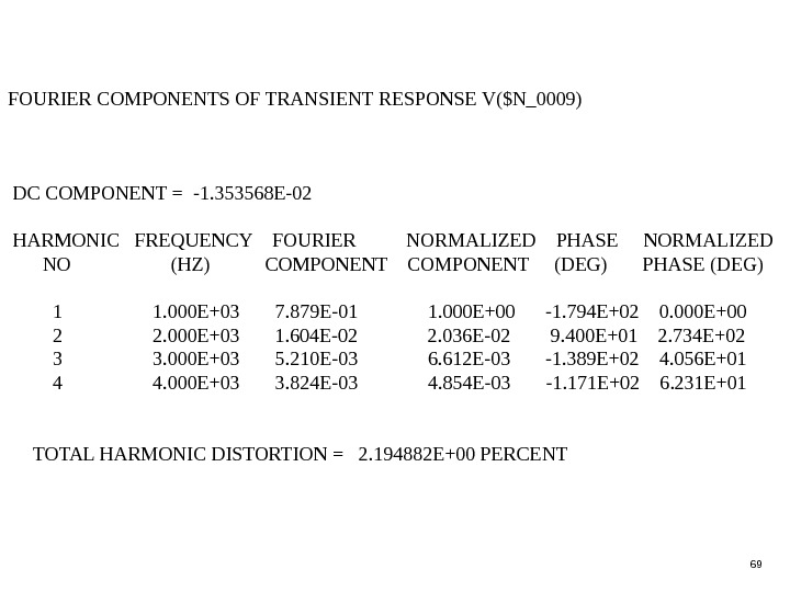
 69 FOURIER COMPONENTS OF TRANSIENT RESPONSE V($N_0009) DC COMPONENT = -1. 353568 E-02 HARMONIC FREQUENCY FOURIER NORMALIZED PHASE NORMALIZED NO (HZ) COMPONENT (DEG) PHASE (DEG) 1 1. 000 E+03 7. 879 E-01 1. 000 E+00 -1. 794 E+02 0. 000 E+00 2 2. 000 E+03 1. 604 E-02 2. 036 E-02 9. 400 E+01 2. 734 E+02 3 3. 000 E+03 5. 210 E-03 6. 612 E-03 -1. 389 E+02 4. 056 E+01 4 4. 000 E+03 3. 824 E-03 4. 854 E-03 -1. 171 E+02 6. 231 E+01 TOTAL HARMONIC DISTORTION = 2. 194882 E+00 PERCENT
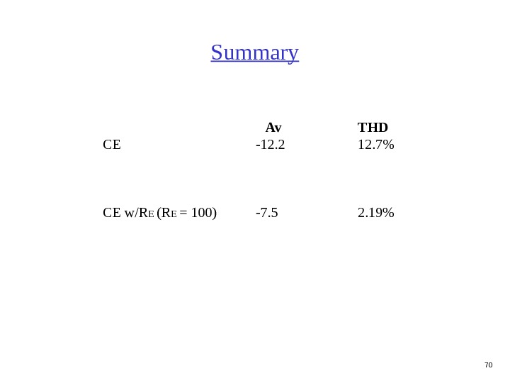
 70 Summary Av THD CE -12. 2 12. 7% CE w/R E (R E = 100) -7. 5 2. 19%
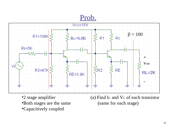
 71 Prob. + v out — • 2 stage amplifier (a) Find I C and V C of each transistor • Both stages are the same (same for each stage) • Capacitively coupled = 100 RL=2 KRc=6. 8 K
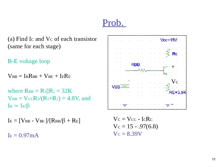
 72 Prob. (a) Find I C and V C of each transistor (same for each stage) B-E voltage loop V BB = I B R BB + V BE + I E R E where R BB = R 1 ||R 2 = 32 K V BB = V CC R 2 /(R 1 +R 2 ) = 4. 8 V, and I B I E / I E = [V BB — V BE ]/[R BB / + R E ] I E = 0. 97 m. A V C = V CC — I C R C V C = 15 -. 97(6. 8) V C = 8. 39 V + V C —
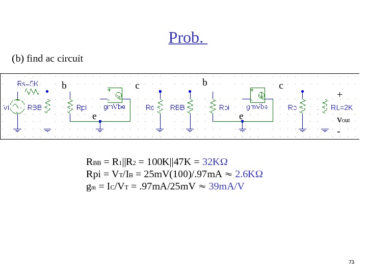
 73 Prob. b c e + v out -(b) find ac circuit b c e R BB = R 1 ||R 2 = 100 K||47 K = 32 K Rpi = V T /I B = 25 m. V(100)/. 97 m. A 2. 6 K g m = I C /V T =. 97 m. A/25 m. V 39 m. A/V RL=2 K
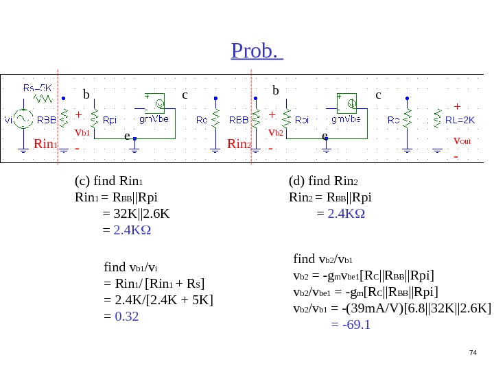
 74 Prob. b c e + v out — (c) find Rin 1 = R BB ||Rpi = 32 K||2. 6 K = 2. 4 K b c e Rin 1 (d) find Rin 2 = R BB ||Rpi = 2. 4 K Rin 2 find v b 1 /v i = Rin 1 / [Rin 1 + R S ] = 2. 4 K/[2. 4 K + 5 K] = 0. 32+ v b 1 — find v b 2 /v b 1 v b 2 = -g m v be 1 [R C ||R BB ||Rpi] v b 2 /v be 1 = -g m [R C ||R BB ||Rpi] v b 2 /v b 1 = -(39 m. A/V)[6. 8||32 K||2. 6 K] = -69. 1+ v b 2 — RL=2 K
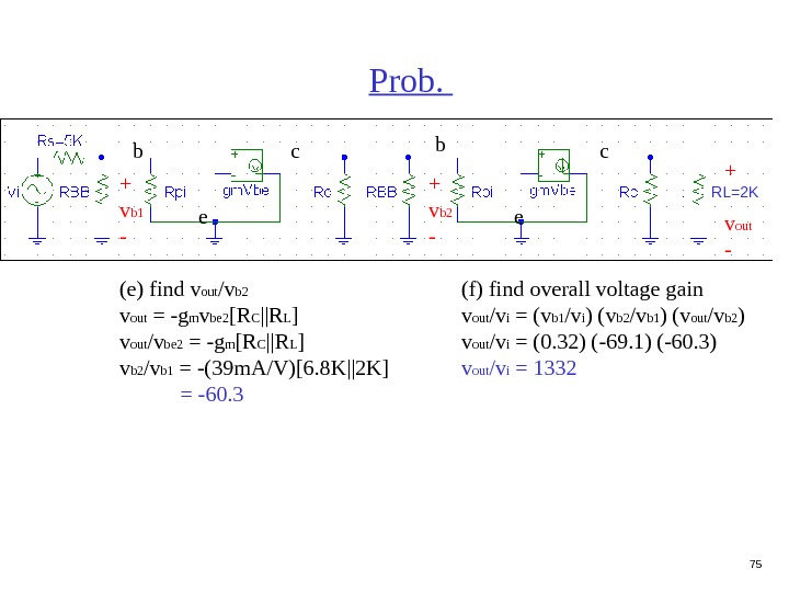
 75 Prob. b c e + v out — (e) find v out /v b 2 v out = -g m v be 2 [R C ||R L ] v out /v be 2 = -g m [R C ||R L ] v b 2 /v b 1 = -(39 m. A/V)[6. 8 K||2 K] = -60. 3 b c e (f) find overall voltage gain v out /v i = (v b 1 /v i ) (v b 2 /v b 1 ) (v out /v b 2 ) v out /v i = (0. 32) (-69. 1) (-60. 3) v out /v i = 1332+ v b 1 — + v b 2 — RL=2 K
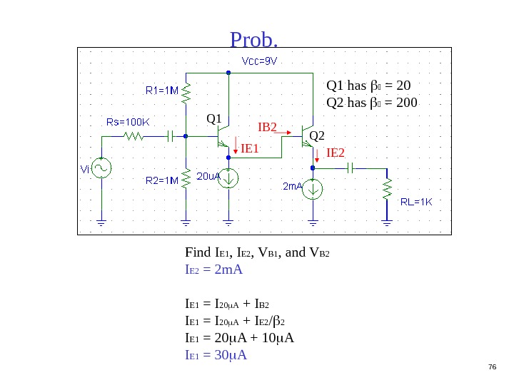
 76 Prob. Find I E 1 , I E 2 , V B 1 , and V B 2 I E 2 = 2 m. A I E 1 = I 20 A + I B 2 I E 1 = I 20 A + I E 2 / 2 I E 1 = 20 A + 10 A I E 1 = 30 A IE 1 IE 2 Q 1 has = 20 Q 2 has = 200 Q 1 Q 2 I
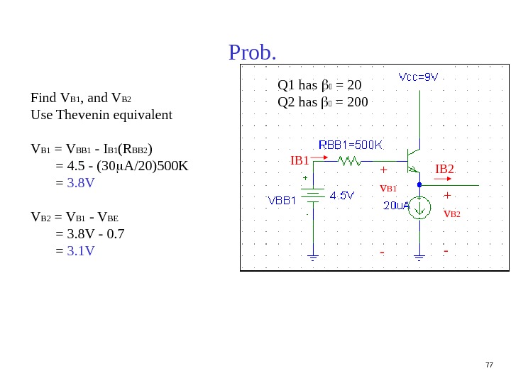
 77 Prob. Find V B 1 , and V B 2 Use Thevenin equivalent V B 1 = V BB 1 — I B 1 (R BB 2 ) = 4. 5 — (30 A/20)500 K = 3. 8 V V B 2 = V B 1 — V BE = 3. 8 V — 0. 7 = 3. 1 V Q 1 has = 20 Q 2 has = 200 IB 2 + v B 1 — + v B 2 -I
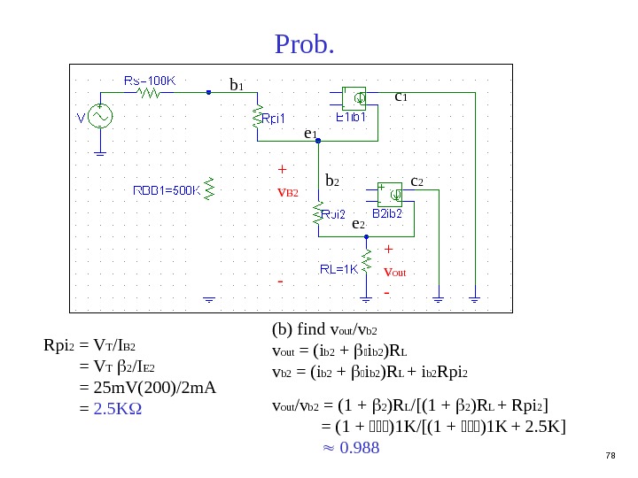
 78 Prob. (b) find v out /v b 2 v out = (i b 2 + i b 2 )R L v b 2 = (i b 2 + i b 2 )R L + i b 2 Rpi 2 v out /v b 2 = (1 + 2 )R L /[(1 + 2 )R L + Rpi 2 ] = (1 + )1 K/[(1 + )1 K + 2. 5 K] 0. 988 b 1 e 1 c 1 b 2 e 2 c 2 + v out -+ v B 2 — Rpi 2 = V T /I B 2 = V T 2 /I E 2 = 25 m. V(200)/2 m. A = 2. 5 K
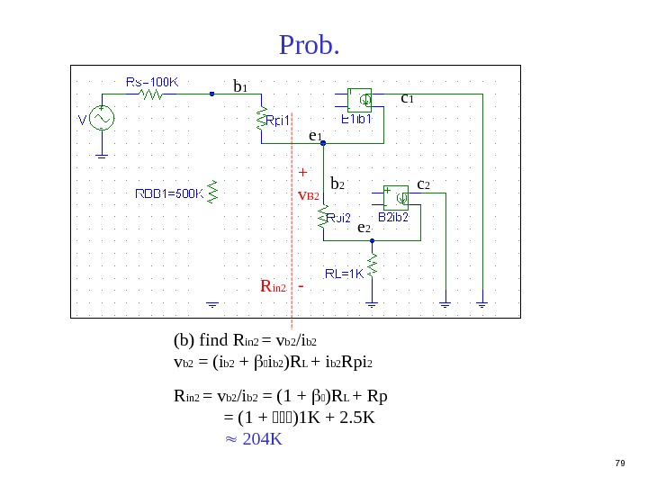
 79 Prob. (b) find R in 2 = v b 2 /i b 2 v b 2 = (i b 2 + i b 2 )R L + i b 2 Rpi 2 R in 2 = v b 2 /i b 2 = (1 + )R L + Rp = (1 + )1 K + 2. 5 K 204 Kb 1 e 1 c 1 b 2 e 2 c 2+ v B 2 — R in
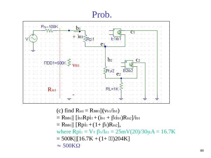
 80 Prob. (c) find R in 1 = R BB 1 ||(v b 1 /i b 1 ) = R BB 1 || [i b 1 Rpi 1 + (i b 1 + i b 1 )R in 2 ]/i b 1 = R BB 1 || [Rpi 1 + (1+ )R in 2 ], where Rpi 1 = V T 1 /I E 1 = 25 m. V(20)/30 A = 16. 7 K = 500 K||[16. 7 K + (1+ )204 K] 500 K b 1 e 1 c 1 b 2 e 2 c 2+ v B 1 -R in 1 i
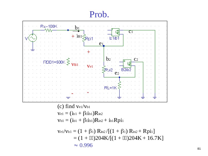
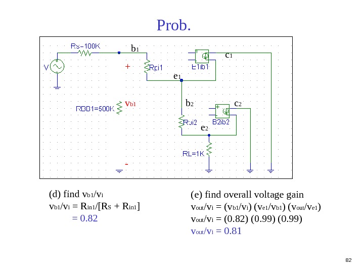
 81 Prob. (c) find v e 1 /v b 1 v e 1 = (i b 1 + i b 1 )R in 2 v b 1 = (i b 1 + i b 1 )R in 2 + i b 1 Rpi 1 v e 1 /v b 1 = (1 + 1 ) R in 2 /[(1 + 1 ) R in 2 + Rpi 1 ] = (1 + )204 K/[(1 + )204 K + 16. 7 K] 0. 996 b 1 e 1 c 1 b 2 e 2 c 2+ v e 1 -i B 1 + v B 1 —
 82 Prob. (d) find v b 1 /v i = R in 1 /[R S + R in 1 ] = 0. 82 b 1 e 1 c 1 b 2 e 2 c 2+ v b 1 — (e) find overall voltage gain v out /v i = (v b 1 /v i ) (v e 1 /v b 1 ) (v out /v e 1 ) v out /v i = (0. 82) (0. 99) v out /v i = 0.
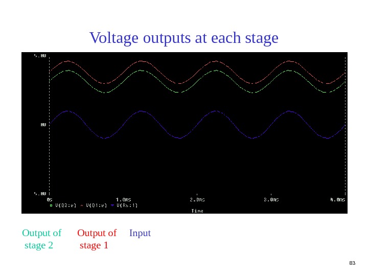
 83 Voltage outputs at each stage Output of stage 2 Output of stage 1 Input
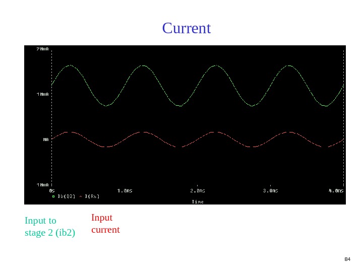
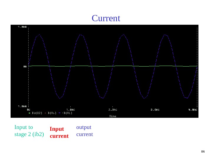
 84 Current Input current. Input to stage 2 (ib 2)
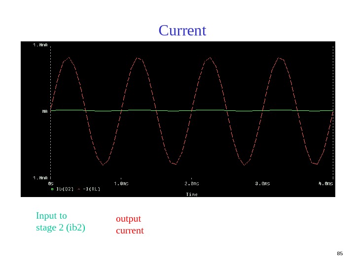
 85 Current output current. Input to stage 2 (ib 2)
 86 Current output current. Input to stage 2 (ib 2) Input current
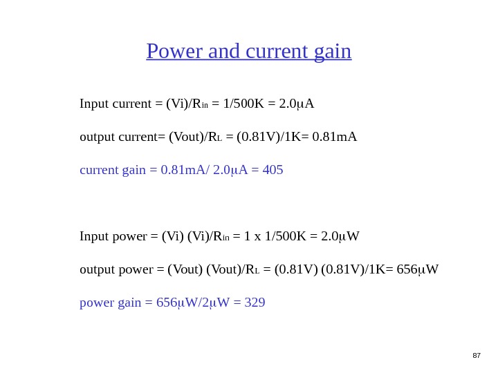
 87 Power and current gain Input current = (Vi)/R in = 1/500 K = 2. 0 A output current= (Vout)/R L = (0. 81 V)/1 K= 0. 81 m. A current gain = 0. 81 m. A/ 2. 0 A = 405 Input power = (Vi)/R in = 1 x 1/500 K = 2. 0 W output power = (Vout)/R L = (0. 81 V)/1 K= 656 W power gain = 656 W/2 W =
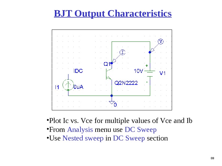
 88 BJT Output Characteristics • Plot Ic vs. Vce for multiple values of Vce and Ib • From Analysis menu use DC Sweep • Use Nested sweep in DC Sweep section
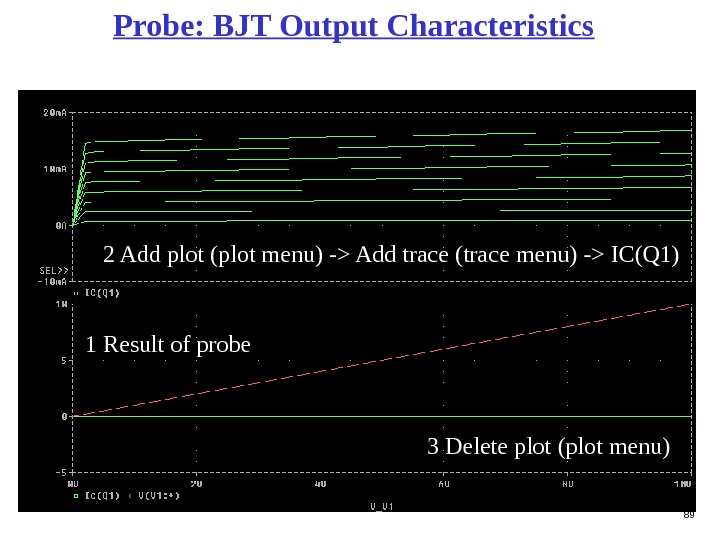
 89 Probe: BJT Output Characteristics 1 Result of probe 2 Add plot (plot menu) -> Add trace (trace menu) -> IC(Q 1) 3 Delete plot (plot menu)
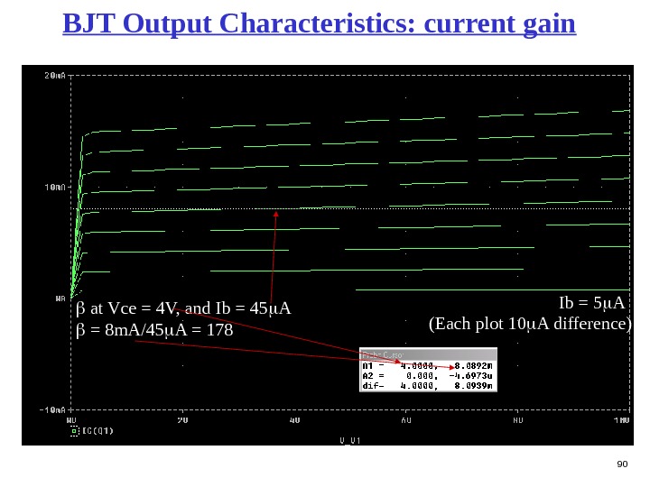
 90 BJT Output Characteristics: current gain Ib = 5 A (Each plot 10 A difference) at Vce = 4 V, and Ib = 45 A = 8 m. A/45 A =
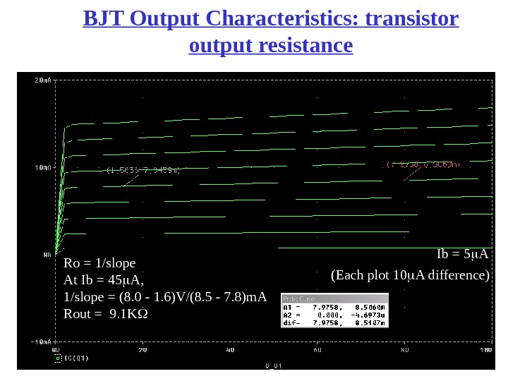
 91 BJT Output Characteristics: transistor output resistance Ib = 5 A (Each plot 10 A difference)Ro = 1/slope At Ib = 45 A, 1/slope = (8. 0 — 1. 6)V/(8. 5 — 7. 8)m. A Rout = 9. 1 K
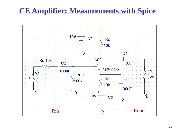
 92 CE Amplifier: Measurements with Spice Rin Rout
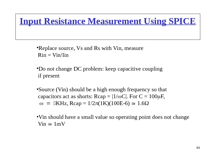
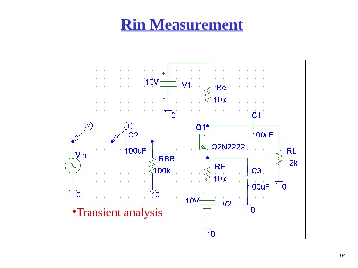
 93 Input Resistance Measurement Using SPICE • Replace source, Vs and Rs with Vin, measure Rin = Vin/Iin • Do not change DC problem: keep capacitive coupling if present • Source (Vin) should be a high enough frequency so that capacitors act as shorts: Rcap = |1/ C|. For C = 100 F, KHz, Rcap = 1/2 (1 K)(100 E-6) 1. 6 • Vin should have a small value so operating point does not change Vin 1 m. V
 94 Rin Measurement • Transient analysis
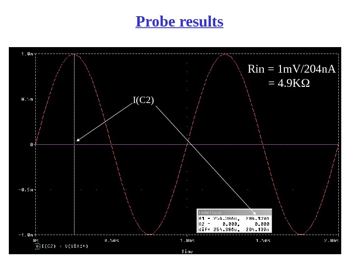
 95 Probe results I(C 2) Rin = 1 m. V/204 n. A = 4. 9 K
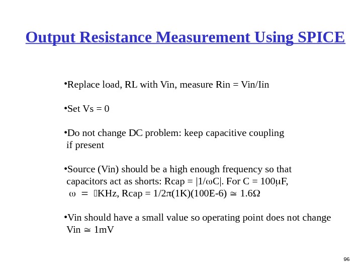
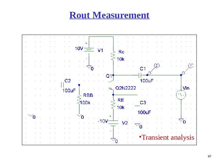
 96 Output Resistance Measurement Using SPICE • Replace load, RL with Vin, measure Rin = Vin/Iin • Set Vs = 0 • Do not change DC problem: keep capacitive coupling if present • Source (Vin) should be a high enough frequency so that capacitors act as shorts: Rcap = |1/ C|. For C = 100 F, KHz, Rcap = 1/2 (1 K)(100 E-6) 1. 6 • Vin should have a small value so operating point does not change Vin 1 m. V
 97 Rout Measurement • Transient analysis
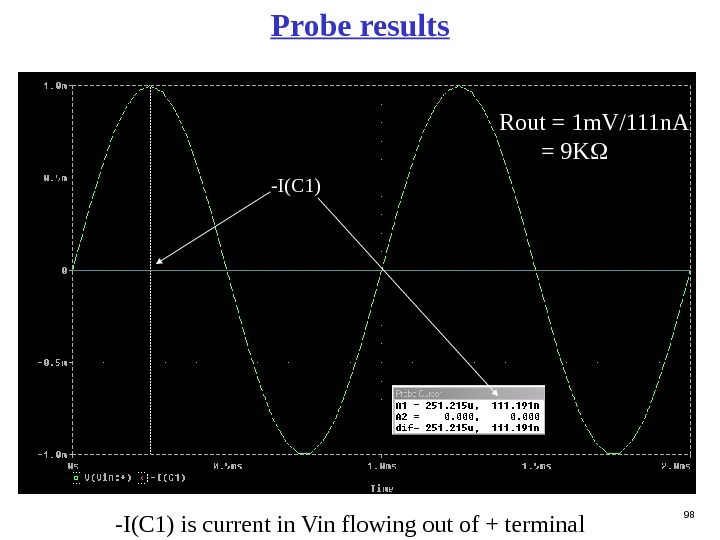
 98 Probe results -I(C 1) Rout = 1 m. V/111 n. A = 9 K -I(C 1) is current in Vin flowing out of + terminal
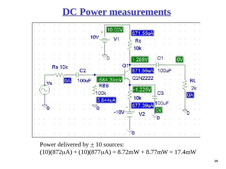
 99 DC Power measurements Power delivered by + 10 sources: (10)(872 A) + (10)(877 A) = 8. 72 m. W + 8. 77 m. W = 17. 4 m. W
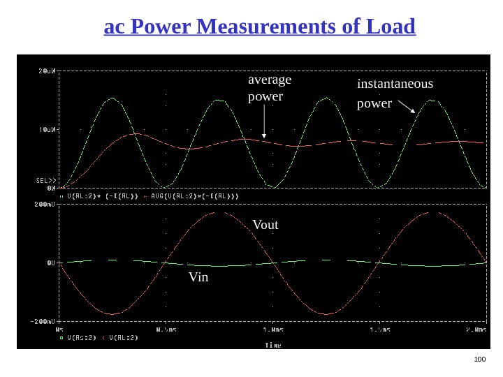
 100 ac Power Measurements of Load instantaneous power average power Vout Vin

