719704ac44e8548d57608d5c8d7166b4.ppt
- Количество слайдов: 55

1 Applications in Particle Physics PSD Themis Bowcock
2 Introduction • Concentrate on applications – Many new ideas in other session – Active R&D for an experiments • Do not attempt to produce exhaustive list – So much exciting work happening – Heavy dependence on electronics • Flavour of some issues… PSD – Highly personal Themis Bowcock
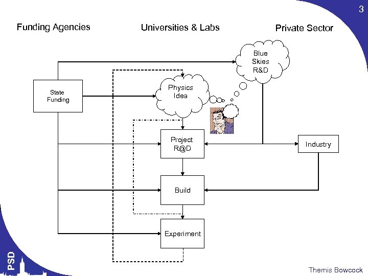
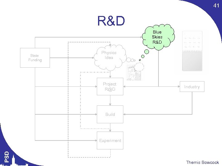
3 Funding Agencies Universities & Labs Private Sector Blue Skies R&D State Funding Physics Idea Project R@D Industry Build PSD Experiment Themis Bowcock
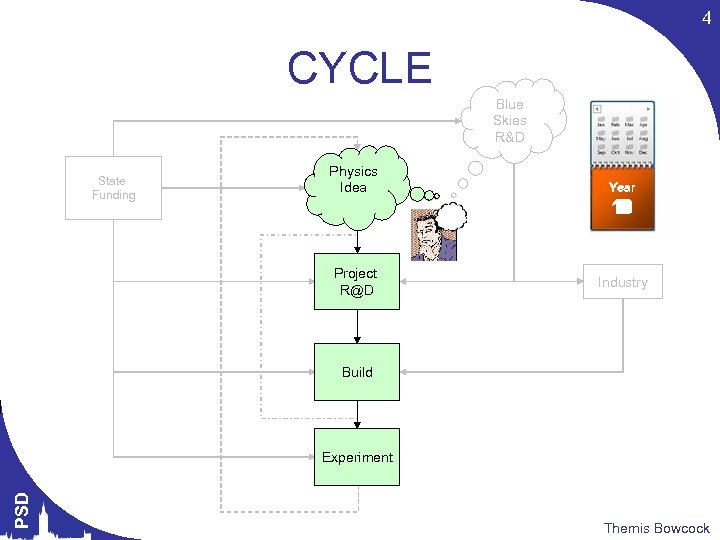
4 CYCLE Blue Skies R&D State Funding Physics Idea Project R@D Year 12 1 0 8 7 6 5 4 11 2 10 3 9 Industry Build PSD Experiment Themis Bowcock
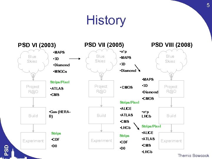
5 History PSD VI (2003) Blue Skies • MAPS • 3 D • Diamond PSD VII (2005) • n+p Blue Skies Project R@D • ATLAS • CMS • 3 D • MAPS Project R@D • CMOS Build • ALICE Build • 3 D • Diamond Strips/Pixel • Gas (HERAB) Blue Skies • MAPS • Diamond • MSGCs Strips/Pixel PSD VIII (2008) • ATLAS Project R@D • CMOS • n+p LHCb Build • CMS • LHCb Strips PSD Experiment • CDF • D 0 Strips/Pixel • ALICE • ATLAS Experiment • CMS • LHCb Themis Bowcock
6 Particle Physics - Last 5 years • Increasing concentration on solid state detectors – In PP less gas • More emphasis on pixels (over strips) – strips engineering issues • Progress on radiation hard Si • Maturing of many technologies – Diamond • Large progress PSD – CMOS Themis Bowcock
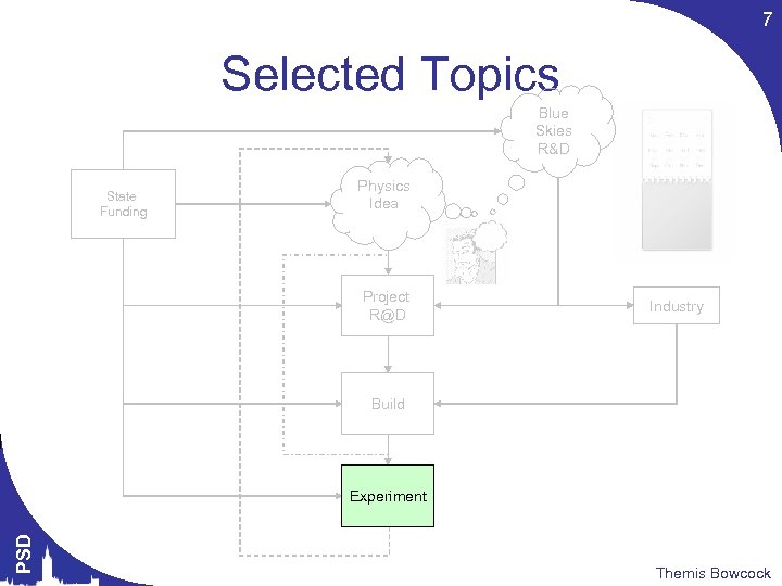
7 Selected Topics Blue Skies R&D State Funding Physics Idea Project R@D Industry Build PSD Experiment Themis Bowcock
8 News from LHC • PSD’s figure highly in recent developments (see Chris Parkes’ talk on opening day) • Commissioning PSD – Cosmic Rays – Synchronization tests – Building up to criculating beam (10 th Sept) Themis Bowcock
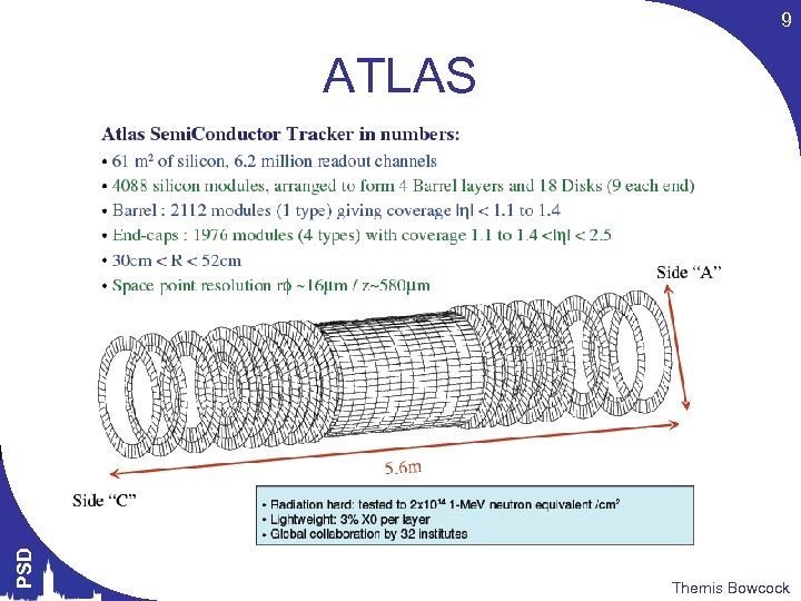
9 PSD ATLAS Themis Bowcock
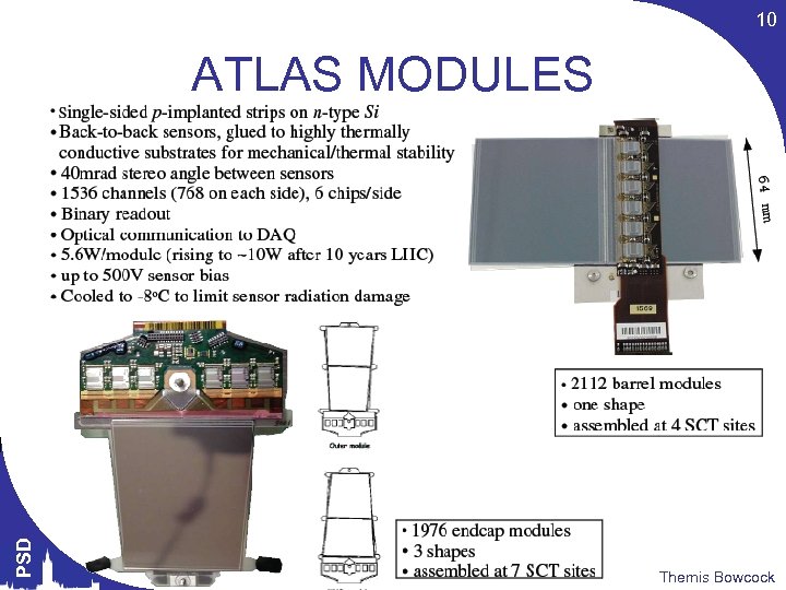
10 PSD ATLAS MODULES Themis Bowcock
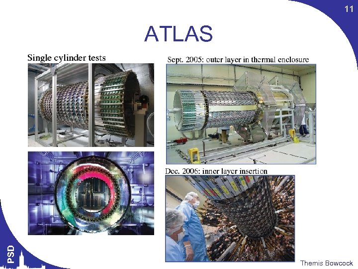
11 PSD ATLAS Themis Bowcock
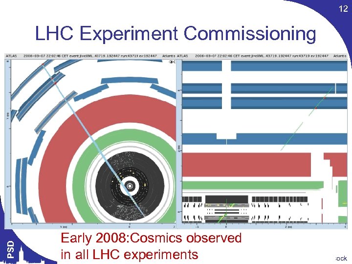
12 PSD LHC Experiment Commissioning Early 2008: Cosmics observed in all LHC experiments Themis Bowcock
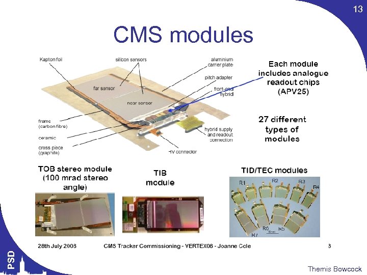
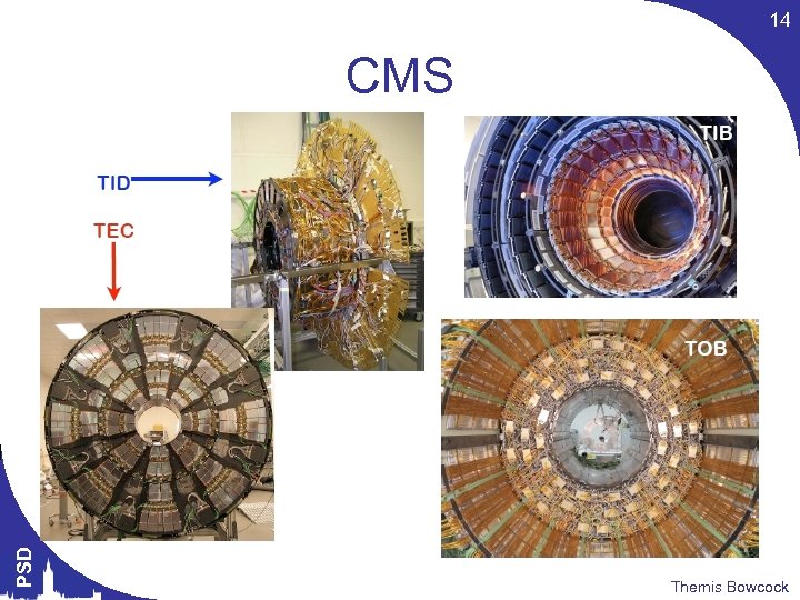
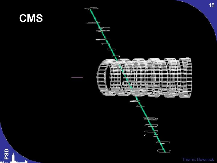
13 PSD CMS modules Themis Bowcock
14 PSD CMS Themis Bowcock
15 PSD CMS Themis Bowcock
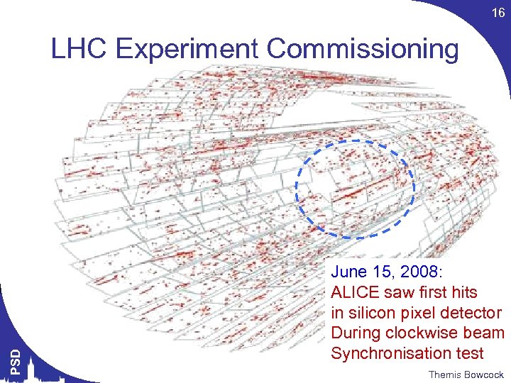
16 PSD LHC Experiment Commissioning June 15, 2008: ALICE saw first hits in silicon pixel detector During clockwise beam Synchronisation test Themis Bowcock
17 3 VELO LHCb injection 6 cm y PSD x Themis Bowcock
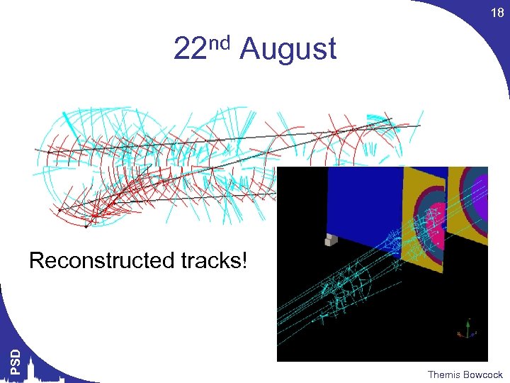
18 22 nd August PSD Reconstructed tracks! Themis Bowcock
19 In a few weeks… PSD • Real tracks and vertices from the next generation of detectors (See the next PSD!) Themis Bowcock
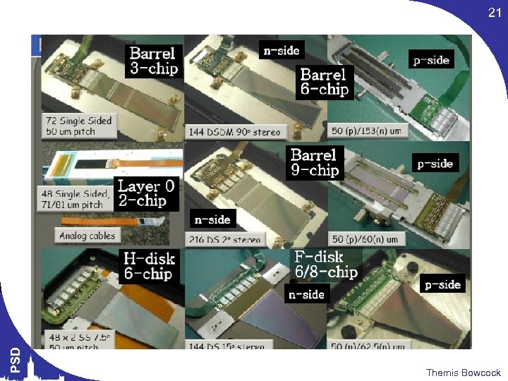
20 Other experiments PSD • D 0 Themis Bowcock
PSD 21 Themis Bowcock
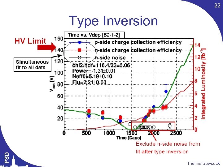
22 PSD Type Inversion Themis Bowcock
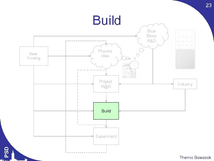
23 Build Blue Skies R&D State Funding Physics Idea Project R@D Industry Build PSD Experiment Themis Bowcock
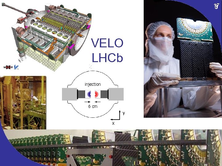
24 Build • The effort to get the CERN experiments ready dominated the last few years – A few builds still in progress PSD • E. g. LHCb “spare” VELO using n+p technlogy Themis Bowcock
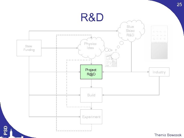
25 R&D Blue Skies R&D State Funding Physics Idea Project R@D Industry Build PSD Experiment Themis Bowcock
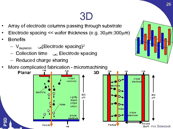
26 3 D • Array of electrode columns passing through substrate • Electrode spacing << wafer thickness (e. g. 30 m: 300 m) • Benefits – Vdepletion (Electrode spacing)2 – Collection time Electrode spacing – Reduced charge sharing • More complicated fabrication - micromachining Planar 3 D +ve -ve +ve n-type electrode electrons 300 µm holes PSD p-type electrode Particle Around 30µm Themis Bowcock
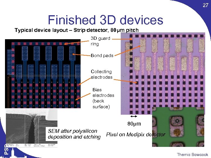
27 Finished 3 D devices Typical device layout – Strip detector, 80μm pitch 3 D guard ring Bond pads Collecting electrodes Bias electrodes (back surface) 80μm PSD SEM after polysilicon deposition and etching Pixel on Medipix detector Themis Bowcock
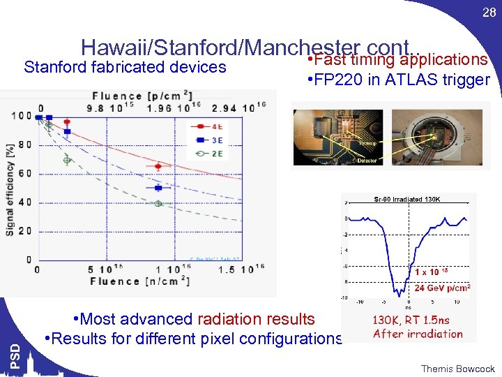
28 Hawaii/Stanford/Manchester cont. . • Fast timing applications PSD Stanford fabricated devices • FP 220 in ATLAS trigger • Most advanced radiation results • Results for different pixel configurations Themis Bowcock
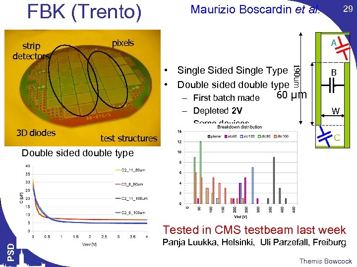
FBK (Trento) strip detectors Maurizio Boscardin et al. A pixels 190 um • Single Sided Single Type • Double sided double type 60 μm – First batch made 3 D diodes test structures 29 – Depleted 2 V – Some devices biased up to 200 V B W C Double sided double type PSD Tested in CMS testbeam last week Panja Luukka, Helsinki, Uli Parzefall, Freiburg Themis Bowcock
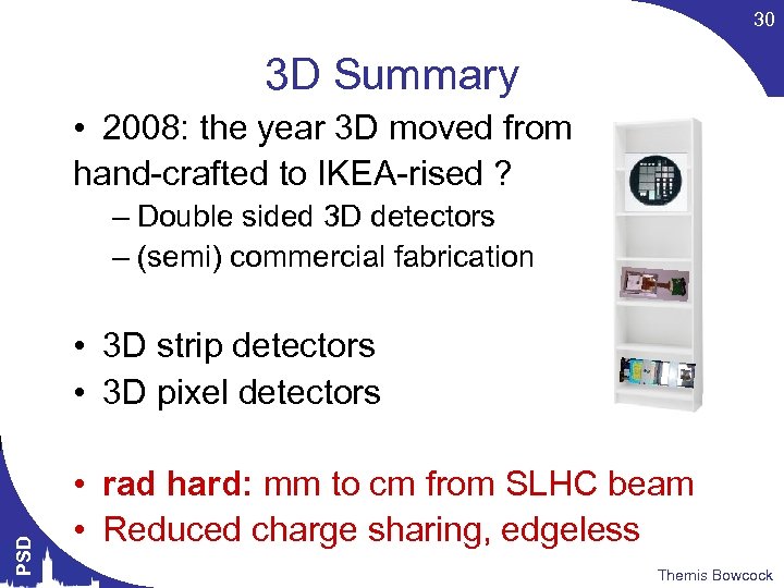
30 3 D Summary • 2008: the year 3 D moved from hand-crafted to IKEA-rised ? – Double sided 3 D detectors – (semi) commercial fabrication PSD • 3 D strip detectors • 3 D pixel detectors • rad hard: mm to cm from SLHC beam • Reduced charge sharing, edgeless Themis Bowcock
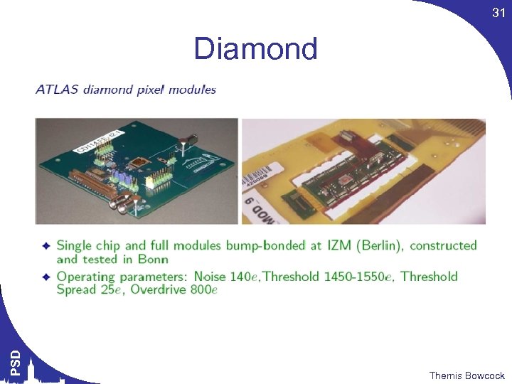
31 PSD Diamond Themis Bowcock
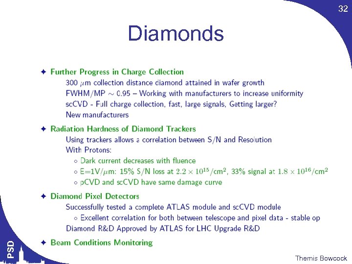
32 PSD Diamonds Themis Bowcock
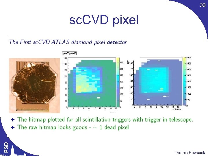
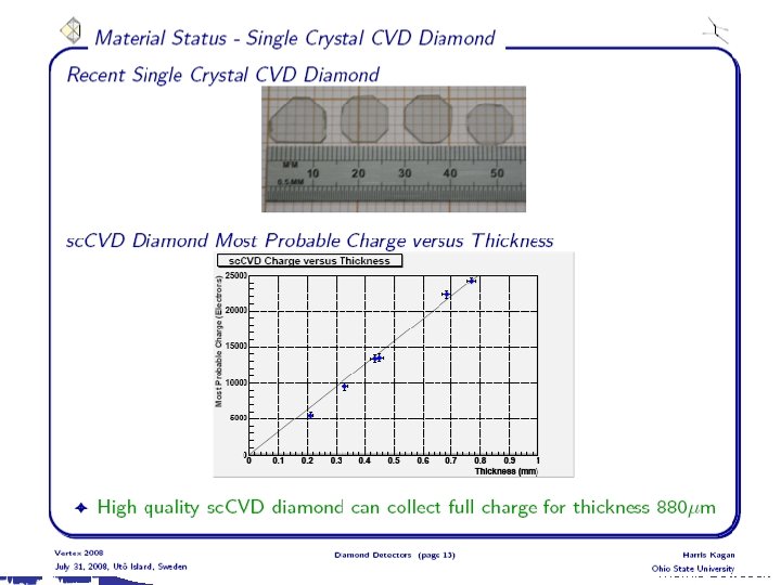
33 PSD sc. CVD pixel Themis Bowcock
PSD 34 Themis Bowcock
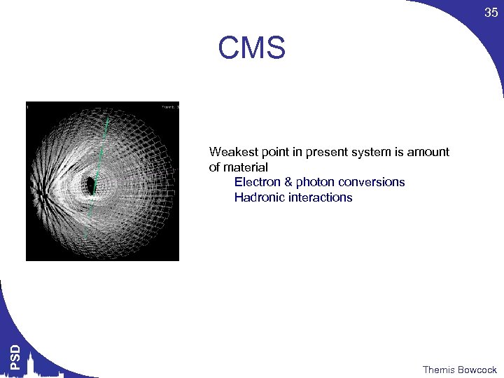
35 CMS PSD Weakest point in present system is amount of material Electron & photon conversions Hadronic interactions Themis Bowcock
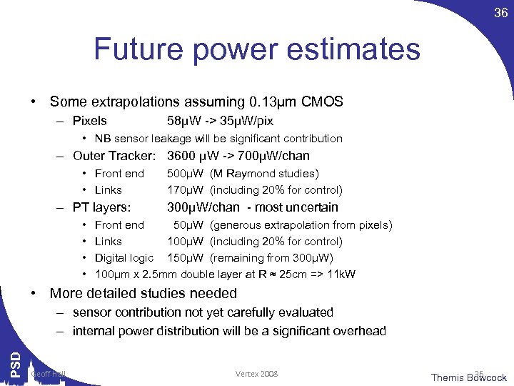
36 Future power estimates • Some extrapolations assuming 0. 13µm CMOS – Pixels 58µW -> 35µW/pix • NB sensor leakage will be significant contribution – Outer Tracker: 3600 µW -> 700µW/chan • Front end • Links – PT layers: • • 500µW (M Raymond studies) 170µW (including 20% for control) 300µW/chan - most uncertain Front end 50µW (generous extrapolation from pixels) Links 100µW (including 20% for control) Digital logic 150µW (remaining from 300µW) 100µm x 2. 5 mm double layer at R ≈ 25 cm => 11 k. W • More detailed studies needed PSD – sensor contribution not yet carefully evaluated – internal power distribution will be a significant overhead Geoff Hall Vertex 2008 36 Themis Bowcock
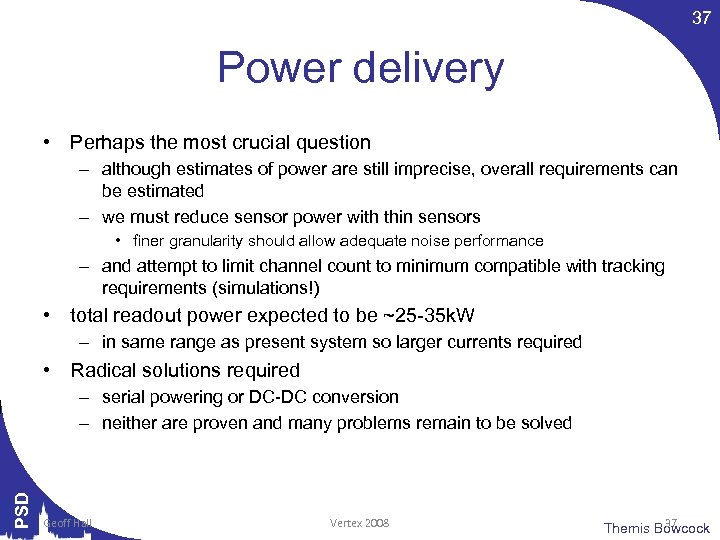
37 Power delivery • Perhaps the most crucial question – although estimates of power are still imprecise, overall requirements can be estimated – we must reduce sensor power with thin sensors • finer granularity should allow adequate noise performance – and attempt to limit channel count to minimum compatible with tracking requirements (simulations!) • total readout power expected to be ~25 -35 k. W – in same range as present system so larger currents required • Radical solutions required PSD – serial powering or DC-DC conversion – neither are proven and many problems remain to be solved Geoff Hall Vertex 2008 37 Themis Bowcock
38 Comment • Reducing power/pixel/strip is a good feature of reduced processing sizes • But increasing density of pixels/strips increases the density PSD – Supply of power and hence requirement of cooling and minimizing mass is now limiting designs Themis Bowcock
39 P-type / ATLAS • p-type detectors most natural solution for e collection on segmented side • n-side read out → lower collection time • No type inversion • No backplane processing • Easier to handle (no need to take care of special gluing on the backside due to the presence of guard-rings. Possibility of operating under-depleted before irradiation) PSD …. and, up to 60% discount with respect to nin-n! • Thin wafers easier Themis Bowcock
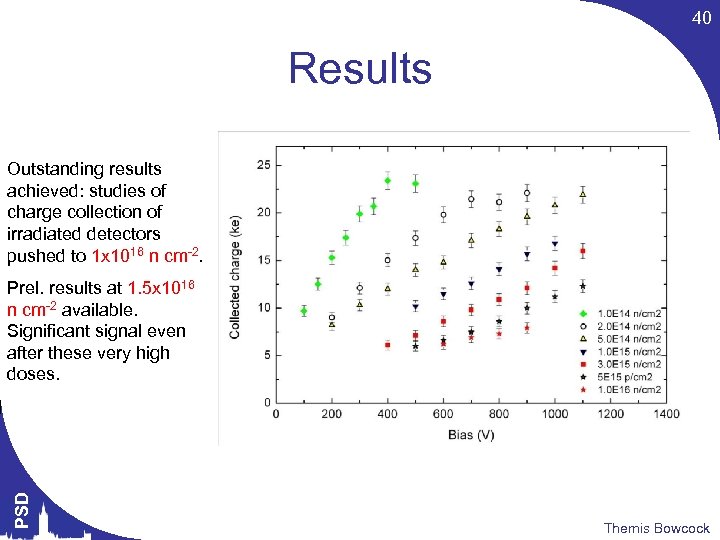
40 Results Outstanding results achieved: studies of charge collection of irradiated detectors pushed to 1 x 10¹⁶ n cm-2. PSD Prel. results at 1. 5 x 10¹⁶ n cm-2 available. Significant signal even after these very high doses. Themis Bowcock
41 R&D Blue Skies R&D State Funding Physics Idea Project R@D Industry Build PSD Experiment Themis Bowcock
42 Driving forces • Future experiments ILC – But also Belle Upgrades – Super-B etc PSD • • High resolution Low mass Radiation tolerance Speed Themis Bowcock
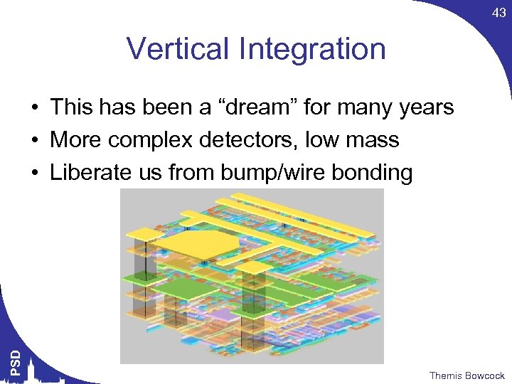
43 Vertical Integration PSD • This has been a “dream” for many years • More complex detectors, low mass • Liberate us from bump/wire bonding Themis Bowcock
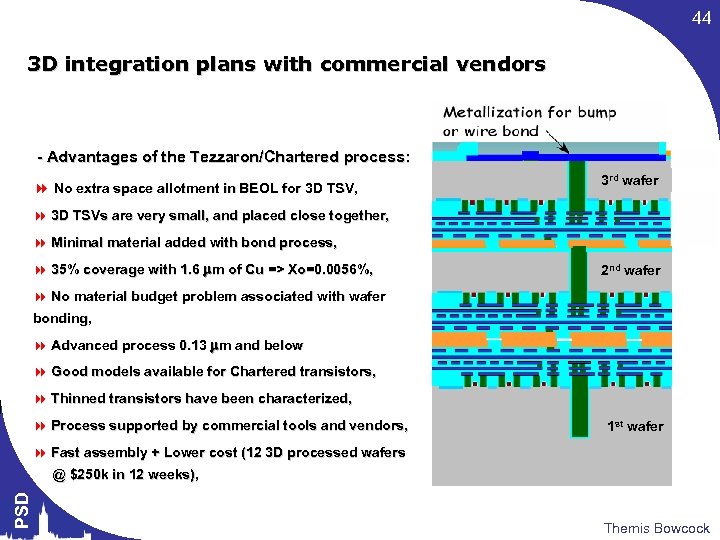
44 3 D integration plans with commercial vendors - Advantages of the Tezzaron/Chartered process: 8 No extra space allotment in BEOL for 3 D TSV, 3 rd wafer 8 3 D TSVs are very small, and placed close together, 8 Minimal material added with bond process, 8 35% coverage with 1. 6 mm of Cu => Xo=0. 0056%, 2 nd wafer 8 No material budget problem associated with wafer bonding, 8 Advanced process 0. 13 mm and below 8 Good models available for Chartered transistors, 8 Thinned transistors have been characterized, 8 Process supported by commercial tools and vendors, 1 st wafer PSD 8 Fast assembly + Lower cost (12 3 D processed wafers @ $250 k in 12 weeks), Themis Bowcock
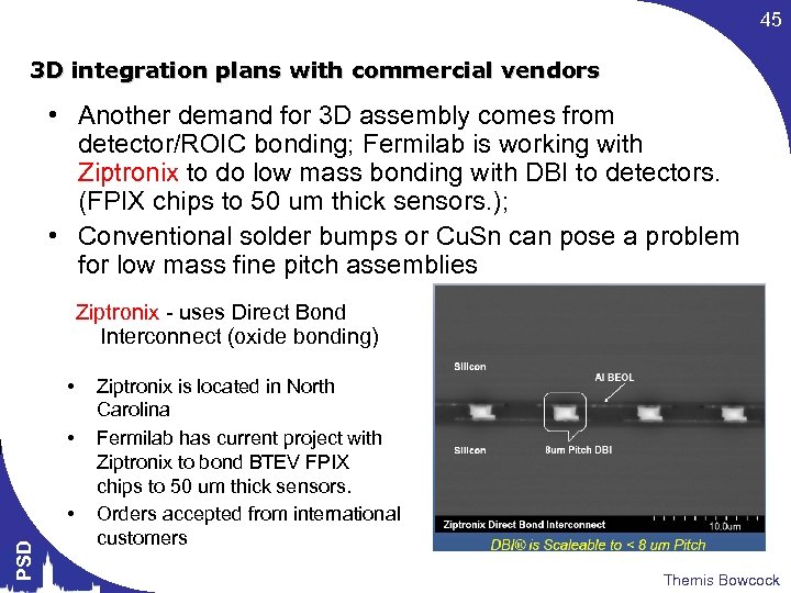
45 3 D integration plans with commercial vendors • Another demand for 3 D assembly comes from detector/ROIC bonding; Fermilab is working with Ziptronix to do low mass bonding with DBI to detectors. (FPIX chips to 50 um thick sensors. ); • Conventional solder bumps or Cu. Sn can pose a problem for low mass fine pitch assemblies Ziptronix - uses Direct Bond Interconnect (oxide bonding) • • PSD • Ziptronix is located in North Carolina Fermilab has current project with Ziptronix to bond BTEV FPIX chips to 50 um thick sensors. Orders accepted from international customers Themis Bowcock
46 Vertical Integration PSD • 3 D Integration is very attractive for highly granular detector systems, • Bonding is low temperature process, adds limited amount of high-Z material, • 3 D-Integration may extend use of certain detector type (MAPS), • 3 D-Integration is starting to be available in industry, • Will our community be able to afford? Themis Bowcock
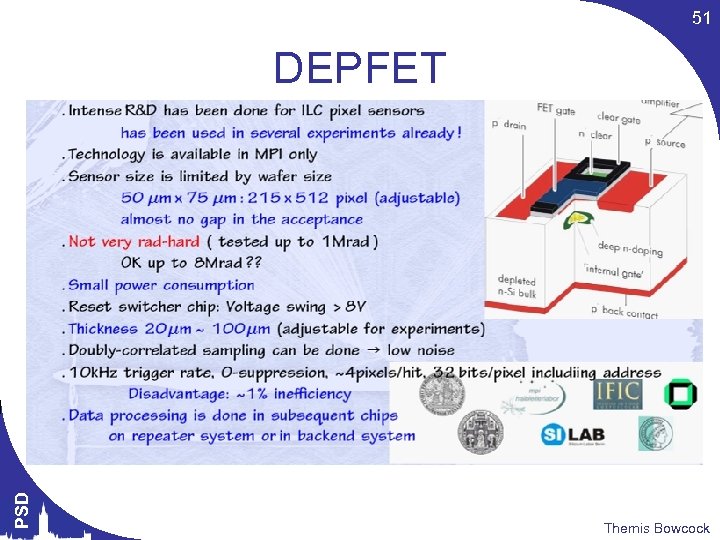
47 Other detectors concepts PSD • • CCDs MAPS and DNW DEPFETs CMOS+SOI Themis Bowcock
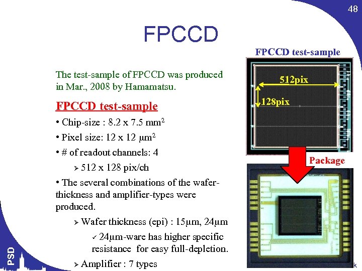
48 FPCCD The test-sample of FPCCD was produced in Mar. , 2008 by Hamamatsu. PSD FPCCD test-sample • Chip-size : 8. 2 x 7. 5 mm 2 • Pixel size: 12 x 12 m 2 • # of readout channels: 4 Ø 512 x 128 pix/ch • The several combinations of the waferthickness and amplifier-types were produced. Ø Wafer thickness (epi) : 15 m, 24 m ü 24 m-ware has higher specific resistance for easy full-depletion. Ø Amplifier : 7 types FPCCD test-sample 512 pix 128 pix Package Themis Bowcock
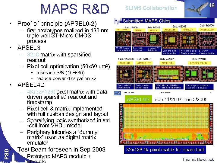
MAPS R&D 49 SLIM 5 Collaboration • Proof of principle (APSEL 0 -2) – first prototypes realized in 130 nm triple well ST-Micro CMOS process • APSEL 3 – 32 x 8 matrix with sparsified readout – Pixel cell optimization (50 x 50 um 2) • Increase S/N (15 30) • reduce power dissipation x 2 • APSEL 4 D – 4 K(32 x 128) pixel matrix with data driven sparsified readout and timestamp – Pixel cell & matrix implemented with full custom design and layout – Sparsifying logic synthetized in std -cell from VHDL model – Periphery inlcudes a “dummy matrix” used as digital matrix emulator PSD • Test Beam foreseen in Sep 2008 – Prototype MAPS module + APSEL 4 D sub 11/2007 - rec 3/2008 32 x 128 4 k pixel matrix for beam test Themis Bowcock
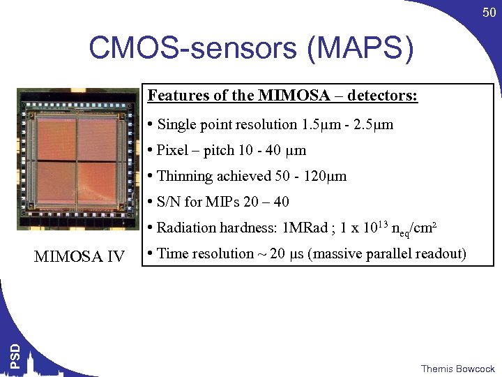
50 CMOS-sensors (MAPS) Features of the MIMOSA – detectors: • Single point resolution 1. 5µm - 2. 5µm • Pixel – pitch 10 - 40 µm • Thinning achieved 50 - 120µm • S/N for MIPs 20 – 40 • Radiation hardness: 1 MRad ; 1 x 10¹³ neq/cm² PSD MIMOSA IV • Time resolution ~ 20 µs (massive parallel readout) Themis Bowcock
51 PSD DEPFET Themis Bowcock
52 A few thoughts • Overestimate 5 year impact and underestimate 20 year impact PSD – Vertical Integration ! Themis Bowcock
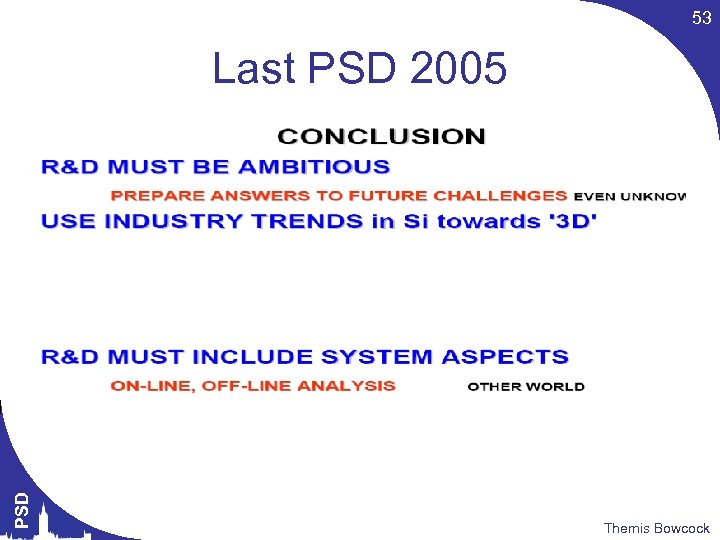
53 PSD Last PSD 2005 Themis Bowcock
54 2008 • Massive Progress in many areas – 3 D – CMOS devices (following industry) – n+p detectors • Smörgåsbord of technological choices – Which ones will make it into detectors? – Practicality and COST! – How many can be used in non HEP applications? • Commissioning of major LHC detectors • Launch of LHC upgrades PSD – Will this boost or stifle R&D? Themis Bowcock
55 Summary • R&D healthy and innovative • Detectors builders worry about prosaic issues – Power – Cost – Material PSD • New paradigms on the horizon… • PSD 9 should be VERY exciting! Themis Bowcock
719704ac44e8548d57608d5c8d7166b4.ppt