08.12.2017 1 Material Aspects of Micro- and Nanoelectromechanical

![08.12.2017 53 Compressive films generally have a mixture of [110] and [311] grains, while 08.12.2017 53 Compressive films generally have a mixture of [110] and [311] grains, while](https://present5.com/presentacii-2/20171208\9790-1-_material_aspects_of_micro-_and_nanoelectromechanical_systems.ppt\9790-1-_material_aspects_of_micro-_and_nanoelectromechanical_systems_53.jpg)
9790-1-_material_aspects_of_micro-_and_nanoelectromechanical_systems.ppt
- Количество слайдов: 56
 08.12.2017 1 Material Aspects of Micro- and Nanoelectromechanical Systems
 08.12.2017 2 Two of the more significant technological achievements during the last 30 years have been the development of MEMS and its new offshoot, NEMS. These developments were made possible by significant advancements in the materials and processes used in the fabrication of MEMS and NEMS devices. And while initial developments capitalized on a mature Si infrastructure, recent advances have used materials and processes not associated with IC fabrication, a trend that is likely to continue as new application areas are identified.
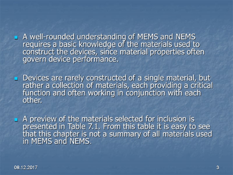
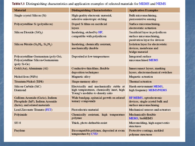
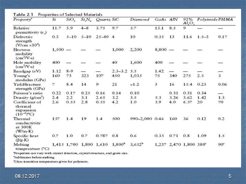
 08.12.2017 3 A well-rounded understanding of MEMS and NEMS requires a basic knowledge of the materials used to construct the devices, since material properties often govern device performance. Devices are rarely constructed of a single material, but rather a collection of materials, each providing a critical function and often working in conjunction with each other. A preview of the materials selected for inclusion is presented in Table 7.1. From this table it is easy to see that this chapter is not a summary of all materials used in MEMS and NEMS.
 08.12.2017 4
 08.12.2017 5
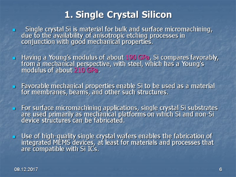
 08.12.2017 6 1. Single Crystal Silicon Single crystal Si is material for bulk and surface micromachining, due to the availability of anisotropic etching processes in conjunction with good mechanical properties. Having a Young’s modulus of about 190 GPa, Si compares favorably, from a mechanical perspective, with steel, which has a Young’s modulus of about 210 GPa. Favorable mechanical properties enable Si to be used as a material for membranes, beams, and other such structures. For surface micromachining applications, single crystal Si substrates are used primarily as mechanical platforms on which Si and non-Si device structures can be fabricated. Use of high-quality single crystal wafers enables the fabrication of integrated MEMS devices, at least for materials and processes that are compatible with Si ICs.
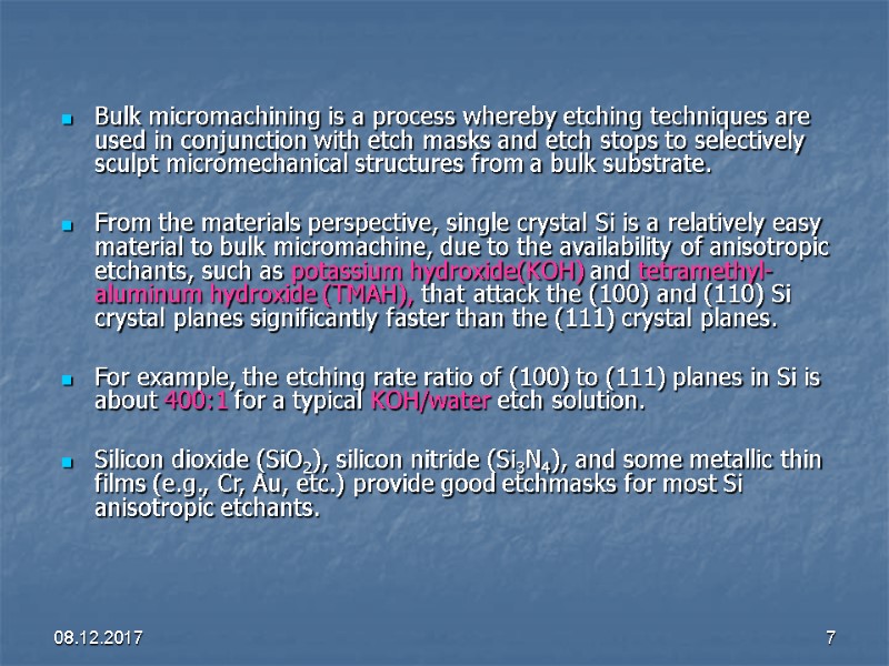
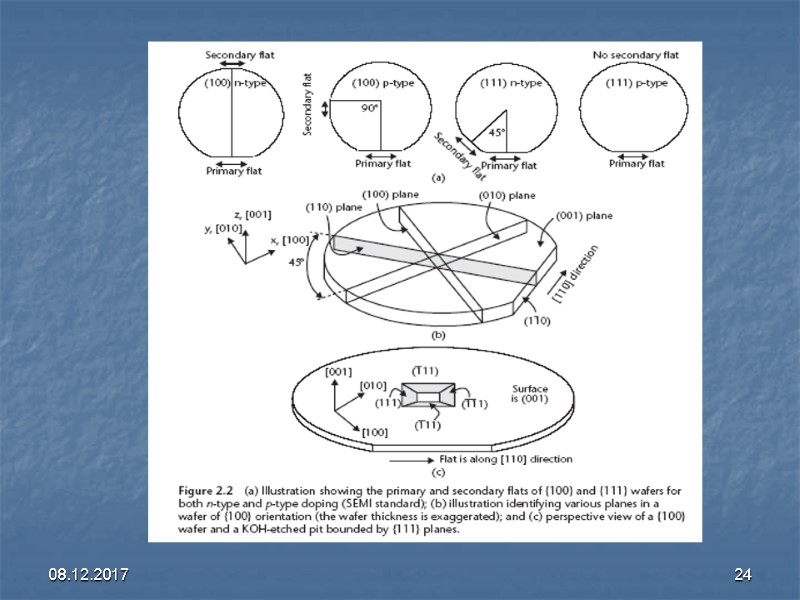
 08.12.2017 7 Bulk micromachining is a process whereby etching techniques are used in conjunction with etch masks and etch stops to selectively sculpt micromechanical structures from a bulk substrate. From the materials perspective, single crystal Si is a relatively easy material to bulk micromachine, due to the availability of anisotropic etchants, such as potassium hydroxide(KOH) and tetramethyl-aluminum hydroxide (TMAH), that attack the (100) and (110) Si crystal planes significantly faster than the (111) crystal planes. For example, the etching rate ratio of (100) to (111) planes in Si is about 400:1 for a typical KOH/water etch solution. Silicon dioxide (SiO2), silicon nitride (Si3N4), and some metallic thin films (e.g., Cr, Au, etc.) provide good etchmasks for most Si anisotropic etchants.
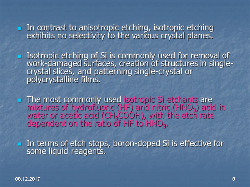
 08.12.2017 8 In contrast to anisotropic etching, isotropic etching exhibits no selectivity to the various crystal planes. Isotropic etching of Si is commonly used for removal of work-damaged surfaces, creation of structures in single-crystal slices, and patterning single-crystal or polycrystalline films. The most commonly used isotropic Si etchants are mixtures of hydrofluoric (HF) and nitric (HNO3) acid in water or acetic acid (CH3COOH), with the etch rate dependent on the ratio of HF to HNO3. In terms of etch stops, boron-doped Si is effective for some liquid reagents.
 08.12.2017 9 Boron-doped etch stops are often less than 10µm thick, since the boron concentration in Si must exceed 7.1019 cm3 for the etch stop to be effective, and the doping is done by diffusion. It is possible to create a boron-doped etch stop below an undoped Si layer using ion implantation; however, the practical implant depth is limited to a few microns.
 08.12.2017 10 Dry etching processes are available to pattern single crystal Si. The process spectrum ranges from physical mechanisms such as sputtering and ion milling to chemical mechanisms such as plasma etching. Reactive ion etching (RIE) is used dry etching technique to etch Si. By combining both physical and chemical processes, RIE is a highly effective anisotropic Si etching technique that is independent of crystalline orientation. Fluorinated compounds such as CF4, SF6, and NF3, or chlorinated compounds such as CCl4 or Cl2, sometimes mixed with He, O2, or H2, are commonly used in Si RIE.
 08.12.2017 11 The RIE process is highly directional, which enables direct pattern transfer from an overlying masking material to the etched Si surface. SiO2 thin films are often used as a masking material, owing to its chemical durability and ease in patterning. Process limitations (i. e., etch rates) restrict the etch depths of Si RIE to less than 10 microns. However, a process called deep reactive ion etching (DRIE) has extended the use of anisotropic dry etching to depths well beyond several hundred microns.
 08.12.2017 12 A wide variety of microfabricated devices have been made from single crystal Si, such as piezoresistive pressure sensors, accelerometers, and mechanical resonators, e.t.c. Using nearly the same approaches but on a smaller scale, top-down nanomachining techniques have been used to fabricate nanoelectromechanical devices from single crystal Si. Single crystal Si is particularly well-suited for nanofabrication, because high crystal quality substrates with very smooth surfaces are readily available.
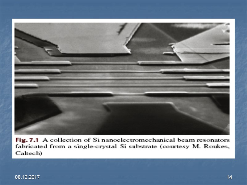
 08.12.2017 13 By coupling electron-beam (e-beam) lithography with conventional Si etching, device structures with submicron dimensions have been fabricated. Submicron, single crystal Si nanomechanical structures have been successfully micromachined from bulk Si wafers and silicon-on-insulator (SOI) wafers. An isotropic Si etch was performed to release the device structures, whereas in the latter (недавний) , the 50 nm to 200 nm structures were released by dissolving the underlying oxide layer in HF. An example of nanoelectromechanical beam structures fabricated from a single crystal Si substrate is shown in Fig. 7.1.
 08.12.2017 14
 08.12.2017 15 In-plane nanoelectromechanical resonators based on silicon nanowire piezoresistive detection E Mile*, G Jourdan*, I Bargatin *+1, S Labarthe *, C Marcoux *, P Andreucci *, S Hentz*, C Kharrat*, E Colinet*, and L Duraffourg* *CEA/LETI MINATEC 17 rue des Martyrs. 38054 GRENOBLE CEDEX 9. +Condensed Matter Physics 114-36, California Institute of Technology, Pasadena, California 91125
 08.12.2017 16 In-plane nanoelectromechanical resonators based on silicon nanowire piezoresistive detection The NEMS device presented in this paper is fabricated using CMOS compatible materials with nano-electronics state-of-the-art lithography and etching techniques. We used a 200-mm silicon-on-insulator (SOI) wafer of (100) orientation with a 160-nm-thick top silicon structural layer (resistivity ≈ 10 Ω·cm) and a 400-nm-thick sacrificial oxide layer.
 08.12.2017 17 The top silicon layer was implanted with boron ions (p-type) through a thin layer of thermal oxide. Homogenous doping (~1019cm-3) in the whole thickness of the top silicon was obtained through specific annealing step (for material reconstruction and doping activation commonly used in CMOS technology), resulting in top layer resistivity of approximately 9 mΩ·cm.
 08.12.2017 18 A hybrid e-beam/DUV lithography technique (allowing 50 nm minimum feature size) was used to define the nano-resonators and electrode pads, respectively. Top silicon layer was etched by anisotropic reactive ion etching (RIE). In order to decrease the lead resistances (сопротивление выводов) , the interconnecting leads have been made thicker with a 650 nm thick AlSi layer, a typical metal for CMOS interconnections process. Finally, the nanoresonators have been released using a vapor HF isotropic etching to remove the sacrificial layer oxide beneath the structures. 1500 devices per wafer of such design are fabricated with this VLSI process. Functionality of the final devices is checked measuring both the lead and gauges resistances and resonant frequency. The yield is 95% per wafer in average.
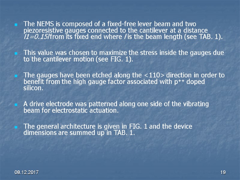
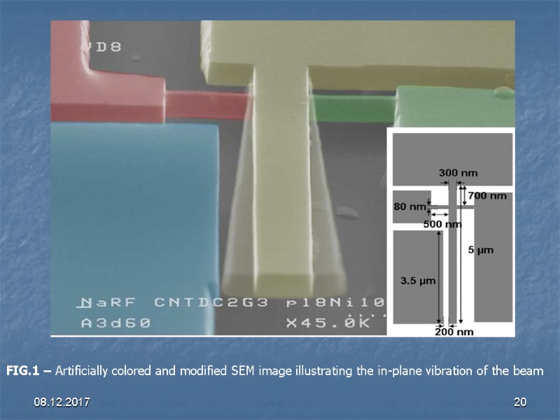
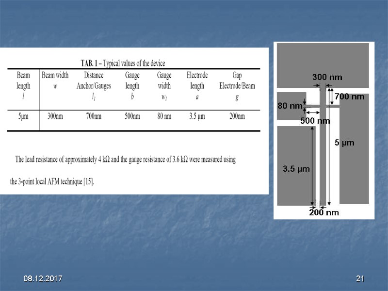
 08.12.2017 19 The NEMS is composed of a fixed-free lever beam and two piezoresistive gauges connected to the cantilever at a distance l1=0.15l from its fixed end where l is the beam length (see TAB. 1). This value was chosen to maximize the stress inside the gauges due to the cantilever motion (see FIG. 1). The gauges have been etched along the <110> direction in order to benefit from the high gauge factor associated with p++ doped silicon. A drive electrode was patterned along one side of the vibrating beam for electrostatic actuation. The general architecture is given in FIG. 1 and the device dimensions are summed up in TAB. 1.
 08.12.2017 20 FIG.1 – Artificially colored and modified SEM image illustrating the in-plane vibration of the beam
 08.12.2017 21
 08.12.2017 22 Silicon as an element exists with three different microstructures: crystalline, polycrystalline, or amorphous. Polycrystalline, or simply “polysilicon,” and amorphous silicon are usually deposited as thin films with typical thicknesses below 5 µm. Crystalline silicon substrates are commercially available as circular wafers with 100-mm (4-in) and 150-mm (6-in) diameters. Larger-diameter (200-mm and 300-mm) wafers, used by the integrated circuit industry, are currently economically unjustified for MEMS. .
 08.12.2017 23 Standard 100-mm wafers are nominally 525 µm thick, and 150-mm wafers are typically 650 µm thick. Double-side-polished wafers commonly used for micromachining on both sides of the wafer are approximately 100 µm thinner than standard thickness substrates. The relatively low cost of these substrates (approximately $10 for a 100-mm-diameter wafer and $15 for a 150-mm wafer) makes them attractive for the fabrication of micromechanical components and systems
 08.12.2017 24
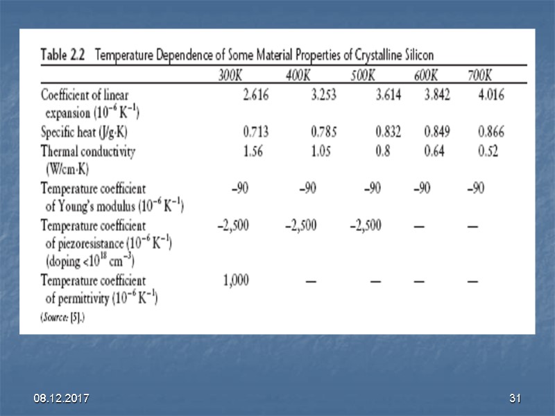
 08.12.2017 25 Silicon is a very good thermal conductor with a thermal conductivity greater than that of many metals and approximately 100 times larger than that of glass. In complex integrated systems, the silicon substrate can be used as an efficient heat sink (поглотитель тепла).
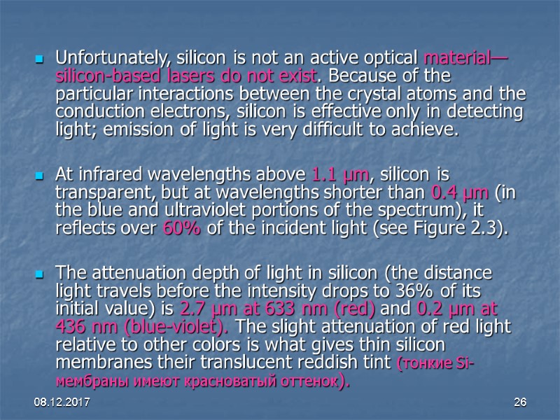
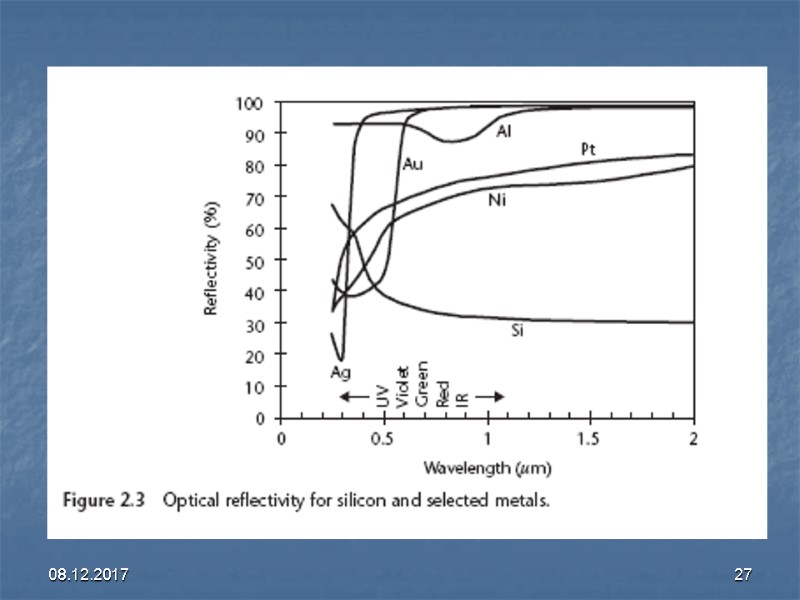
 08.12.2017 26 Unfortunately, silicon is not an active optical material—silicon-based lasers do not exist. Because of the particular interactions between the crystal atoms and the conduction electrons, silicon is effective only in detecting light; emission of light is very difficult to achieve. At infrared wavelengths above 1.1 µm, silicon is transparent, but at wavelengths shorter than 0.4 µm (in the blue and ultraviolet portions of the spectrum), it reflects over 60% of the incident light (see Figure 2.3). The attenuation depth of light in silicon (the distance light travels before the intensity drops to 36% of its initial value) is 2.7 µm at 633 nm (red) and 0.2 µm at 436 nm (blue-violet). The slight attenuation of red light relative to other colors is what gives thin silicon membranes their translucent reddish tint (тонкие Si-мембраны имеют красноватый оттенок).
 08.12.2017 27
 08.12.2017 28 Silicon is also well known to retain its mechanical integrity at temperatures up to about 700°C . At higher temperatures, silicon starts to soften and plastic deformation can occur under load. While the mechanical and thermal properties of polysilicon are similar to those of single crystal silicon, polysilicon experiences slow stress annealing effects at temperatures above 250°C, making its operation at elevated temperatures subject to long-term instabilities, drift, and hysteresis effects. The surface of silicon oxidizes immediately upon exposure to the oxygen in air (referred to as native oxide). The oxide thickness self-limits at a few nanometers at room temperature. As silicon dioxide is very inert, it acts as a protective layer that prevents chemical reactions with the underlying silicon.
 08.12.2017 29 The interactions of silicon with gases, chemicals, biological fluids, and enzymes (ферменты) remain the subject of many research studies, but, for the most part, silicon is considered stable and resistant to many elements and chemicals typical of daily applications. For example, experiments have shown that silicon remains intact (неповреждённый) in the presence of Freon™ gases as well as automotive fluids such as brake fluids (тормозная жидкость). Silicon has also proven to be a suitable material for applications such as valves for the delivery of ultra-high-purity gases.
 08.12.2017 30 In medicine and biology, studies are ongoing to evaluate silicon for medical implants. Preliminary medical evidence indicates that silicon is benign (доброкачественный) in the body and does not release toxic substances when in contact with biological fluids; however, it appears from recent experiments that bare silicon surfaces may not be suitable for high-performance polymerase chain reactions (PCR) intended (предназначенный) for the amplification of genetic DNA material. The polymerase chain reaction (PCR) is a biochemical technology in molecular biology to amplify a single or a few copies of a piece of DNA across several orders of magnitude, generating thousands to millions of copies of a particular DNA sequence.
 08.12.2017 31
 08.12.2017 32 Polysilicon Surface micromachining is a process whereby a sequence of thin films, often of different materials, is deposited and selectively etched to form the desired micromechanical structure. In contrast to bulk micromachining, the substrate serves primarily as a platform to support the device. For Si-based surface micromachined MEMS, Si*-polysilicon is most often used as the structural material, silicon dioxide (SiO2) as the sacrificial material, silicon nitride (Si3N4) for electrical isolation of device structures, and single crystal Si as the substrate.
 08.12.2017 33 Like single crystal Si, polysilicon can be doped during or after film deposition. SiO2 can be thermally grown or deposited on Si over a broad temperature range (e.g., 200 ◦C to 1,150 ◦C) to meet various process and material requirements.
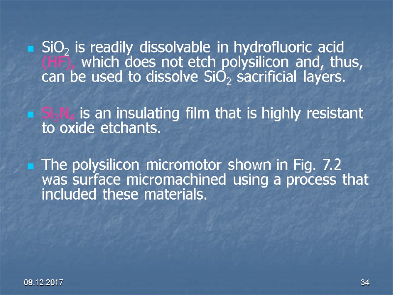
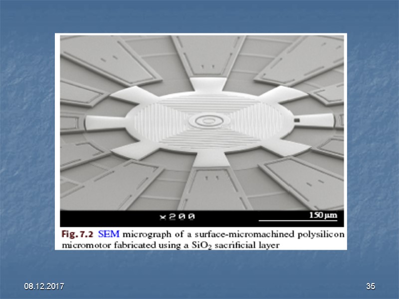
 08.12.2017 34 SiO2 is readily dissolvable in hydrofluoric acid (HF), which does not etch polysilicon and, thus, can be used to dissolve SiO2 sacrificial layers. Si3N4 is an insulating film that is highly resistant to oxide etchants. The polysilicon micromotor shown in Fig. 7.2 was surface micromachined using a process that included these materials.
 08.12.2017 35
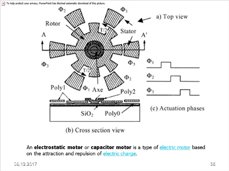
 08.12.2017 36 An electrostatic motor or capacitor motor is a type of electric motor based on the attraction and repulsion of electric charge.
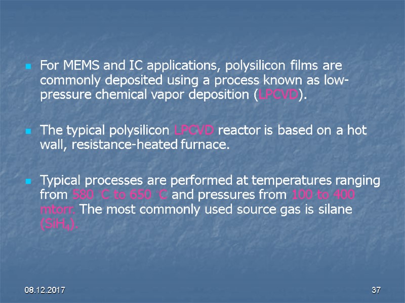
 08.12.2017 37 For MEMS and IC applications, polysilicon films are commonly deposited using a process known as low-pressure chemical vapor deposition (LPCVD). The typical polysilicon LPCVD reactor is based on a hot wall, resistance-heated furnace. Typical processes are performed at temperatures ranging from 580 ◦C to 650 ◦C and pressures from 100 to 400 mtorr. The most commonly used source gas is silane (SiH4).
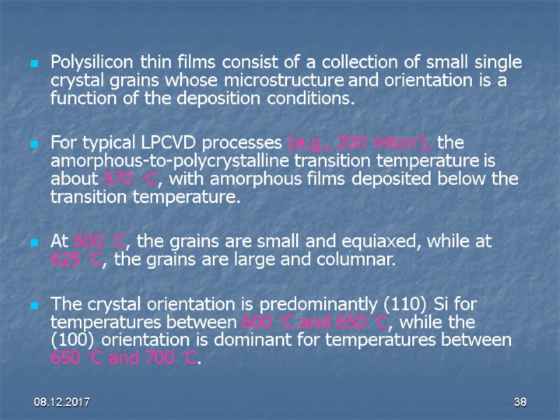
 08.12.2017 38 Polysilicon thin films consist of a collection of small single crystal grains whose microstructure and orientation is a function of the deposition conditions. For typical LPCVD processes (e.g., 200 mtorr), the amorphous-to-polycrystalline transition temperature is about 570 ◦C, with amorphous films deposited below the transition temperature. At 600 ◦C, the grains are small and equiaxed, while at 625 ◦C, the grains are large and columnar. The crystal orientation is predominantly (110) Si for temperatures between 600 ◦C and 650 ◦C, while the (100) orientation is dominant for temperatures between 650 ◦C and 700 ◦C.
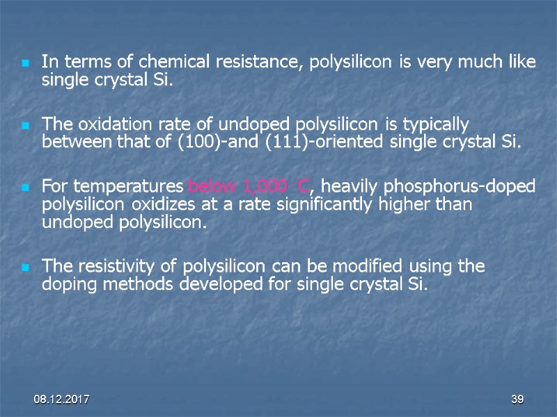
 08.12.2017 39 In terms of chemical resistance, polysilicon is very much like single crystal Si. The oxidation rate of undoped polysilicon is typically between that of (100)-and (111)-oriented single crystal Si. For temperatures below 1,000 ◦C, heavily phosphorus-doped polysilicon oxidizes at a rate significantly higher than undoped polysilicon. The resistivity of polysilicon can be modified using the doping methods developed for single crystal Si.
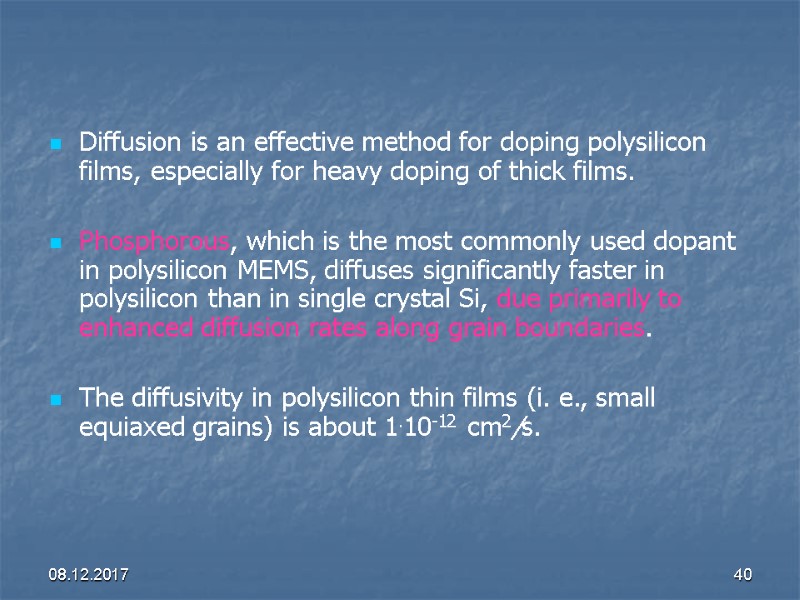
 08.12.2017 40 Diffusion is an effective method for doping polysilicon films, especially for heavy doping of thick films. Phosphorous, which is the most commonly used dopant in polysilicon MEMS, diffuses significantly faster in polysilicon than in single crystal Si, due primarily to enhanced diffusion rates along grain boundaries. The diffusivity in polysilicon thin films (i. e., small equiaxed grains) is about 1.10-12 cm2/s.
 08.12.2017 41 Ion implantation is also used to dope polysilicon films. A high-temperature annealing step is usually required to electrically activate the implanted dopants, as well as to repair implant-related damage in the polysilicon films. In general, the conductivity of implanted polysilicon films is not as high as films doped by diffusion. In situ doping of polysilicon is performed by simply including a dopant gas, usually diborane (B2H6) or phosphine (PH3), in the CVD process.
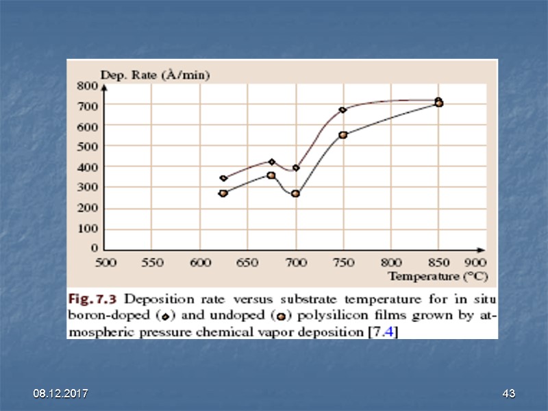
 08.12.2017 42 The addition of dopants during the deposition process not only modifies the conductivity, but also affects the deposition rate of the polysilicon films. As shown in Fig. 7.3, the inclusion of boron generally increases the deposition rate of polysilicon relative to undoped films, while phosphorus (not shown) reduces the rate. In situ doping can be used to produce conductive films with uniform doping profiles without requiring the high-temperature steps usually associated with diffusion or ion implantation.
 08.12.2017 43
 08.12.2017 44 Although commonly used to produce doped polysilicon for electrostatic devices, Cao et al. have used in situ phosphorus-doped polysilicon films in piezoresistive strain gauges, achieving gauge factors as high as 15 for a single strip sensor. The thermal conductivity of polysilicon is a strong function of its microstructure and, therefore, the conditions used during deposition. For fine-grained (мелкозернистый) films, the thermal conductivity is about 25% of the value of single crystal Si.
 08.12.2017 45 For thick films with large grains, the thermal conductivity ranges between 50% and 85% of the single crystal value. Like the electrical and thermal properties of polysilicon, the as-deposited residual stress in polysilicon films depends on microstructure. For films deposited under typical conditions (200 mtorr, 625 ◦C), the as-deposited polysilicon films have compressive residual stresses. The highest compressive stresses are found in amorphous Si films and polysilicon films with a strong, columnar (110) texture. For films with fine-grained microstructures, the stress tends to be tensile.
 08.12.2017 46 Annealing can be used to reduce the compressive stress in as-deposited polysilicon films. For instance, compressive residual stresses on the order of 500 MPa can be reduced to less than 10 MPa by annealing the as-deposited films at 1,000 ◦C in a N2 ambient. Recent advances in the area of rapid thermal annealing (RTA) indicate that RTA provides an effective method of stress reduction in polysilicon films.
 08.12.2017 47 Zhang et al. reported that a 10 s anneal at 1,100 ◦C was sufficient to completely relieve the stress in films that originally had a compressive stress of about 340 MPa. RTA is particularly attractive in situations where the process parameters require a low thermal budget.
 08.12.2017 48 As an alternative to high-temperature annealing, Yang et al. have developed an approach that actually utilizes the residual stress characteristics of polysilicon deposited under various conditions to construct polysilicon multilayers that have the desired thickness and stress values. The multilayers are comprised (заключать в себе) of alternating tensile and compressive polysilicon layers that are deposited in a sequential manner.
 08.12.2017 49 The tensile layers consist of fine-grained polysilicon grown at a temperature of 570 ◦C, while the compressive layers are made up of columnar polysilicon deposited at 615 ◦C. The overall stress in the composite film depends on the number of alternating layers and the thickness of each layer. With the proper set of parameters, a composite polysilicon multilayer can be deposited with near zero residual stress and no stress gradient.
 08.12.2017 50 The process achieves stress reduction reduction without high-temperature annealing, a considerable advantage for integrated MEMS processes. Many device designs require thick polysilicon structural layers that are not readily achievable using conventional LPCVD polysilicon, due to process-related limitations. For these designs, epitaxial Si reactors can be used to grow polysilicon films.
 08.12.2017 51 Unlike conventional LPCVD processes with deposition rates of less than 100A/min, epitaxial processes have deposition rates on the order of 1micron/min. The high deposition rates result from the much higher substrate temperatures (> 1,000 ◦C) and deposition pressures (> 50 torr) used in these processes. The polysilicon films are usually deposited on SiO2 sacrificial layers to enable surface micromachining.
 08.12.2017 52 An LPCVD polysilicon seed layer is sometimes used to control nucleation, grain size, and surface roughness. As with conventional polysilicon, the microstructure and residual stress of the epi-poly films, as they are known, is related to deposition conditions.
![>08.12.2017 53 Compressive films generally have a mixture of [110] and [311] grains, while >08.12.2017 53 Compressive films generally have a mixture of [110] and [311] grains, while](https://present5.com/presentacii-2/20171208\9790-1-_material_aspects_of_micro-_and_nanoelectromechanical_systems.ppt\9790-1-_material_aspects_of_micro-_and_nanoelectromechanical_systems_53.jpg) 08.12.2017 53 Compressive films generally have a mixture of [110] and [311] grains, while tensile films have a random mix of [110], [100], [111], and [311] grains. The Young’s modulus of epi-poly measured from micromachined test structures is comparable to LPCVD polysilicon. Mechanical properties test structures, thermal actuators, electrostatically actuated accelerometers, and gyroscopes have been fabricated from these films.
08.12.2017 53 Compressive films generally have a mixture of [110] and [311] grains, while tensile films have a random mix of [110], [100], [111], and [311] grains. The Young’s modulus of epi-poly measured from micromachined test structures is comparable to LPCVD polysilicon. Mechanical properties test structures, thermal actuators, electrostatically actuated accelerometers, and gyroscopes have been fabricated from these films.
 08.12.2017 54 All of the aforementioned (вышеупомянутые) polysilicon deposition processes utilize substrate temperatures in excess (превышение) of 570 ◦C either during film deposition, or in postdeposition processing steps. As a low temperature alternative to LPCVD polysilicon, Abe et al. and Honer et al. have developed sputtering processes for polysilicon. Early work emphasized the ability to deposit very smooth (25 A) polysilicon films on thermally oxidized wafers at reasonable deposition rates (191 A/min) and with low residual compressive stresses. tdep=7.8 s
 08.12.2017 55 The process involved DC magnitron sputtering from a Si target using an Ar sputtering gas, a chamber pressure of 5mtorr, and a power of 100 W. The authors reported that a post-deposition anneal at 700 ◦C in N2 for two hours was needed to crystallize the deposited film and perhaps lower the stress. Honer et al. sought to develop a polymer-friendly, Si-based surface micromachining process based on polysilicon sputtered onto polyimide and PSG sacrificial layers. To improve the conductivity of the micromachined Si structures, the sputtered Si films were sandwiched between two TiW cladding layers (оболочка) .
 08.12.2017 56 The device structures on polyimide were released using oxygen plasma etching. The processing step with the highest temperature was, in fact, the polyimide cure at 350 ◦C. To test the robustness of the process, sputter-deposited Si microstructures were fabricated on substrates containing CMOS devices. As expected from thermal budget considerations, the authors reported no measurable degradation of device performance.

