
04/01/16 11 Porous Silicon Porous


2-_material_aspects_of_micro-_and_nanoelectromechanical_systems.ppt
- Размер: 2.1 Mегабайта
- Количество слайдов: 80
Описание презентации 04/01/16 11 Porous Silicon Porous по слайдам
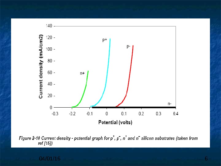
04/01/16 11 Porous Silicon Porous Si is produced by room temperature electrochemical etching of Si in HF. If configured as an electrode in an HF-based electrochemical circuit, positive charge carriers (holes) at the Si surface facilitate the exchange of F atoms with H atoms , that terminate the Si surface. The exchange continues in the subsurface region, leading to the eventual removal of the fluorinated Si. . The quality of the etched surface is related to the density of holes at the surface, which is controlled by the applie d d current density.
04/01/
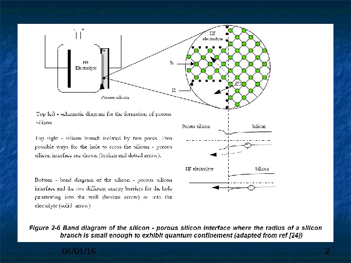
04/01/16 3 Suggested mechanism for the electrochemical dissolution of silicon
04/01/
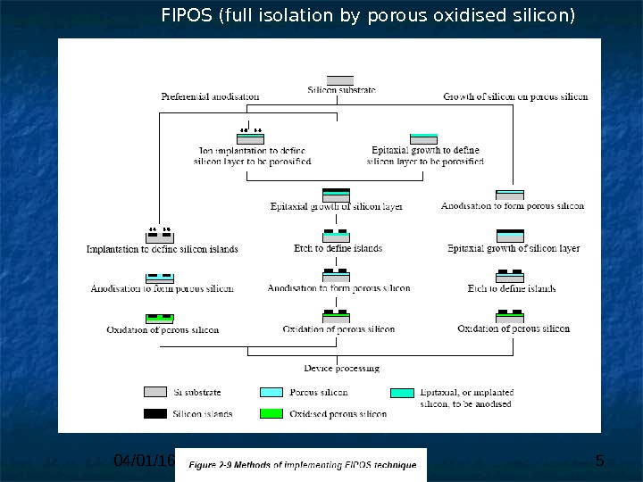
04/01/16 5 FIPOS (full isolation by porous oxidised silicon)
04/01/
04/01/16 7 Fundamentals of Porous Silicon Preparation. Prof. Dr. Michael J. Sailor. Published Online: 13 JAN 2012. DOI: 10. 1002/9783527641901. ch 1. Copyright © 2012. . .
04/01/16 8 The techniques employed for dielectric isolation using porous silicon can also be used for micromachining applications. Micromachining is used to fabricate small-scale mechanical devices that are integrated with conventional microelectronics. Examples of micromachined devices include motors , cantilevers and a wide variety of sensors that are designed to sense temperature , IR and UV radiation, fluid flow or gas flow. Many of these structures are fabricated on free-standing membranes, structures that can be easily fabricated using porous silicon.
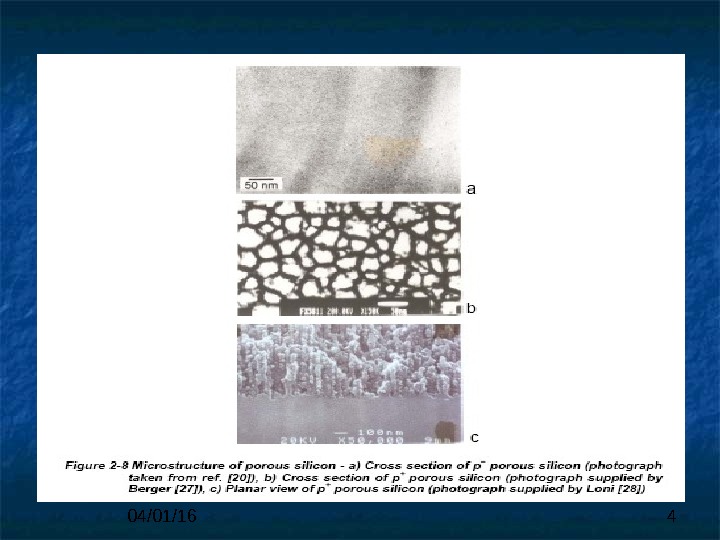
04/01/16 9 For high current densities, the density of holes is high and the etched surface is smooth. For lowlow current densities, the hole density is lowlow and clustered in in highly localized regions associated with surfac e e defects. . Surface defects become enlarged by etching, which leads to to the formation of pores. Pore size and density are related to the type of Si used and the conditions of the electrochemical cell. Both single crystal and polycrystalline Si can be converted to porous Si.
04/01/16 10 The large surface-to-volume ratios make porous Si attractive for gaseous and liquid applications, including filter membranes and absorbing layers for chemical and mass sensing. When single crystal substrates are used, the unetched porous layer remains single crystalline and is suitable for epitaxial Si Si growth. CVD coatings do not generally penetrate the porous regions, but rather overcoat the pores at the surface of the substrate. The formation of localized Si-on-insulator structures is possible by combining pore formation with epitaxial growth, followed by dry etching to create access (доступ) holes to the porous region, and thermal oxidation of the underlying porous region.
04/01/16 11 A third application uses porous Si as a sacrificial layer for polysilicon and single crystalline Si Si surface micromachining. As shown by Lang et al. , the process involves the electrical isolation of the solid structural Si layer by by either pp — n-junction formation through selective doping, oror use of electrically insulating thin films, since the formation of pores only occurs on electrically charged surfaces. A weak Si etchant will aggressively attack the porous regions with little damage to the structural Si layers and can be used to to release the devices.
04/01/16 12 Silicon Dioxide Silicon dioxide (Si. O 22 ) is one of the most widely used materials in the fabrication of MEMS. In polysilicon surface micromachining, Si. O 22 is is used as a sacrificial material, since it can be easily dissolved using etchants that do not attack polysilicon. Si. O 22 is widely used as etch mask for dry etching of thick polysilicon films, since it is chemically resistant to dry etching processes for polysilicon. Si. O 22 films are also used as passivation layers on on the surfaces of environmentally sensitive devices.
04/01/16 13 The most common processes used to produce Si. O 22 films for polysilicon surface micromachining are thermal oxidation and LPCVD. Thermal oxidation of Si is performed at temperatures of 900 ◦◦ CC to to 11 , , 200 ◦◦ CC in the presence of oxygen or steam. Since thermal oxidation is a self-limiting process , , the maximum practical film thickness that can be obtained is about 2µm , which is sufficient for many sacrificial applications. TT hermal oxidation of Si can only be performed on on Si surfaces.
04/01/16 14 Si. O 22 films can be deposited on a wide variety of substrate materials by LPCVD provides aa means for depositing thick (( > > 2µm) Si. O 22 films at temperatures much lower than thermal oxidation. Known as low-temperature oxides ( ( LTOLTO )) , , these films have a higher etch rate in HF than thermal oxides, which translates to significantly faster release times when LTO films are used as sacrificial layers.
04/01/16 15 Phosphosilicate glass (PSG) can be formed using nearly the same deposition process as LTO by adding a phosphorus-containing gasgas to the precursor flows. PSGPSG films are useful as sacrificial layers, since they generally have higher etching rates in HF than LTOLTO films
04/01/16 16 PSG and LTO films are deposited in hot-wall, lowlow pressure, fused silica furnaces in systems similar to those described previously for polysilicon. Precursor gases include Si. H 44 as a Si source, OO 22 as an oxygen source, and, in the case of PSG, PHPH 33 as a source of phosphorus. LTOLTO and PSG films are typically deposited at temperatures of 425 ◦◦ C to 450 ◦◦ CC and pressures ranging from 200 mtorr to 400 mtorr.
04/01/16 17 The low deposition temperatures result in LTO and PSG films that are slightly less dense than thermal oxides, due to the incorporation of of hydrogen in the films. LTO films can, however, be densified by an annealing step at high temperature (1(1 , , 000 ◦◦ C). The low density of LTO and PSG films is partially responsible for the increased etch rate in HF.
04/01/16 18 Thermal Si. O 22 and LTO are electrical insulators used in numerous MEMS applications. The dielectric constants of thermal oxide and LTO are 33. . 99 and 44. . 33 , , respectively. The dielectric strength of thermal Si. O 22 is is 11. . 1010 66 V V // cmcm , and for LTO it is about 80%80% of of that value. The stress in thermal Si. O 22 is compressive with a magnitude of about 300 MPa.
04/01/16 19 For LTOLTO the as-deposited residual stress is tensile , , with a magnitude of about 100 MPa to to 400 MPa. The addition of phosphorous to LTO decreases the tensile residual stress to about 10 MPa for phosphorus concentrations of 8%. As with polysilicon, the properties of LTO and PSG are dependent on processing conditions.
04/01/16 20 Plasma-enhanced chemical vapor deposition (PECVD) is is another common method to produce oxides of silicon. Using a plasma to dissociate the gaseous precursors , , thethe deposition temperatures needed to deposit PECVD oxide films is lower than for LPCVD films. For this reason, PECVD oxides are quite commonly used as masking, passivation, and protective layers, especially on devices that have been coated with metals.
04/01/16 21 Quartz is the crystalline form of Si. O 22 and has interesting properties for MEMS. Quartz is optically transparent, piezoelectric, and electrically insulating. Like single crystal Si, quartz substrates are available as high quality, large area wafers that can be bulk micromachined using anisotropic etchants. Quartz has recently become a popular substrate material for microfluidic devices due to its optical, electronic, and chemical properties.
04/01/16 22 Another Si. O 22 -related material that has recently found uses in MEMS is spin-on-glass (SOG). SOG is a a polymeric material with a viscosity suitable for spin coating. Two recent publications illustrate the potential for SOG in MEMS fabrication. In the first example, Yasseen et al. detailed the development of SOG as a a thick-film sacrificial molding material for thick polysilicon films. The authors reported a process to deposit, polish, and etch SOG films that were 20 microns thick. .
04/01/16 23 The thick SOGSOG films were patterned into molds and filled with 10 micron-thick LPCVD polysilicon films, planarized by by selective CMPCMP , and subsequently dissolved in a wet etchant containing HCl, HF, and HH 22 O to reveal (обнажить) the patterned polysilicon structures. The cured (отвержденная) SOG films were completely compatible with the polysilicon deposition process.
04/01/16 24 In the second example, Liu et al. ff abricated high-aspect ratio channel plate microstructures from SOG. Electroplated nickel (Ni) was used as a molding material , with Ni channel plate molds fabricated using a conventional LIGA process. The Ni. Ni molds were then filled with SOG, and the sacrificial Ni molds were removed in a reverse electroplating process. In this case, the fabricated SOG structures ( over 100 microns tall) were micromachined glass structures fabricated using a molding material more commonly used for structural components.
04/01/16 25 Thick (5– 100 µm) spin-on glass (SOG) has the ability to uniformly coat surfaces and smooth out underlying topographical variations, effectively planarizing surface features. Thin (0. 1– 0. 5 µm) SOG was heavily investigated in the integrated circuit industry as an interlayer dielectric between metals for high-speed electrical interconnects; however, its electrical properties are considered poor compared to thermal or CVD silicon oxides.
04/01/16 26 Spin-on glass is commercially available in different forms, commonly siloxane- or silicate-based. The latter type allows water absorption into the film, resulting in a higher relative dielectric constant and a tendency to crack. After deposition, the layer is typically densified at a temperature between 300º and 500ºC. Measured film stress is approximately 200 MPa in tension but decreases substantially with increasing anneal temperatures. There are two basic types of SOG : siloxane-based organic SOG and silicate — based inorganic SOG.
04/01/16 27 Spin on glass (SOG) is a mixture of Si. O 2 2 and dopants (either boron or phosphorous) that is suspended in a solvent solution. . The SOG is applied to a clean silicon wafer by spin-coating just like photoresist.
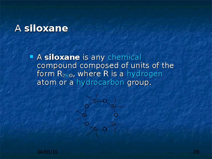
04/01/16 28 A A siloxanesiloxane is any chemical compound composed of units of the form R 22 Si. Si OO , where R is a hydrogen atom or a hydrocarbon group.
04/01/16 29 MDn. M: polydimethylsiloxane. D 6: dodecamethylcyclohexasilox aneane MD 2 M: decamethyltetrasiloxane. D 5: decamethylcyclopentasiloxa nene MDM: octamethyltrisiloxane. D 4: octamethylcyclotetrasiloxan ee MM: hexamethyldisiloxan ee. D 3: hexamethylcyclotrisiloxane Linear siloxanes Cyclic siloxanes An e xamples are : [Si. O(CH 3 ) 2 ] n ( polydimethylsiloxane ) and [Si. O(C 6 H 5 ) 2 ] n ( polydiphenylsiloxane ).
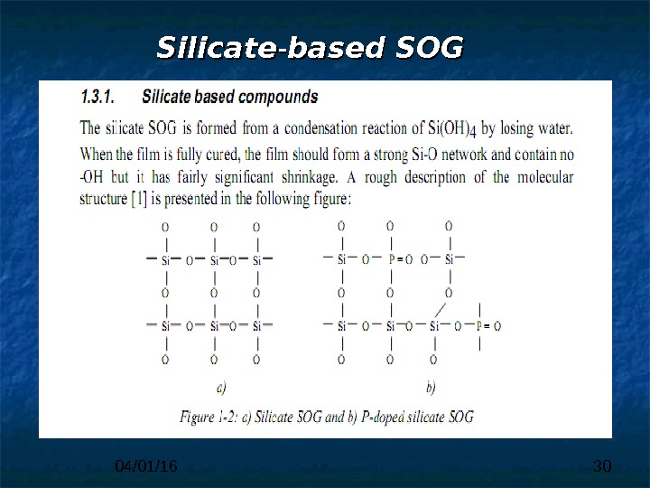
04/01/16 30 SS ilicate — based SOG
04/01/16 31 Silicon Nitride Silicon nitride (Si(Si 33 NN 44 )) is is widely used in MEMS for electrical isolation, surface passivation, etch masking, and as a mechanical material. Two deposition methods are commonly used to deposit Si. Si 33 NN 44 thin films: LPCVD and PECVD. . .
04/01/16 32 PECVD silicon nitride is generally nonstoichiometric (sometimes denoted as Si. Si xx NN y y : H: H ) ) andand may contain significant concentrations of hydrogen. Use of PECVD silicon nitride in micromachining applications is somewhat limited because it has a high etch rate in HFHF (e. g. , often higher than that of thermally grown Si. O 22 ). ). However, PECVD offers the ability to deposit nearly stress-free silicon nitride films, an attractive property for encapsulation and packaging. .
04/01/16 33 Unlike its PECVD counterpart, LPCVD Si. Si 33 NN 44 is is extremely resistant to chemical attack, making it the material of choice for many Si bulk and surface micromachining applications. LPCVD Si. Si 33 NN 44 is commonly used as an insulating layer because it has a resistivity of of 1010 1616 Ω Ω cmcm and field breakdown limit of 1010 77 V V // cm. LPCVD Si. Si 33 NN 44 films are deposited in horizontal furnaces similar to those used for polysilicon deposition.
04/01/16 34 Typical deposition temperatures and pressures range between 700 ◦◦ C to 900 ◦◦ C C and 200 mtorr to 500 mtorr , respectively. The standard source gases are dichlorosilane (Si. H 22 Cl. Cl 22 )) and ammonia (NH(NH 33 )) , , tt o produce stoichiometric Si. Si 33 NN 44 , a NH 33 to to Si. H 22 Cl. Cl 22 ratio of 10: 1 is commonly used. The microstructure of films deposited under these conditions is amorphous. .
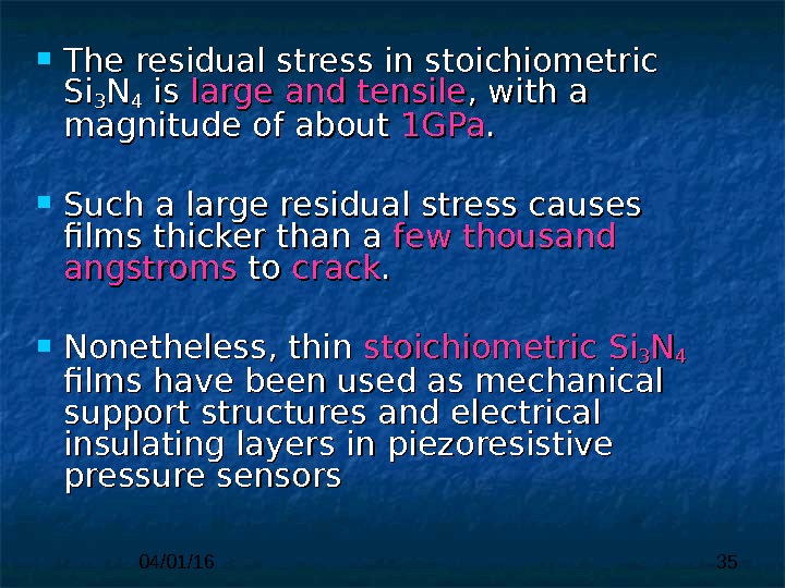
04/01/16 35 The residual stress in stoichiometric Si. Si 33 NN 44 is is large and tensile , with a magnitude of about 1 GPa. . Such a large residual stress causes films thicker than a fewfew thousand angstroms to to crack. . Nonetheless, thin stoichiometric Si. Si 33 NN 44 films have been used as mechanical support structures and electrical insulating layers in piezoresistive pressure sensors
04/01/16 36 Стехиометрия (от(от др. -греч. . στοιχεῖον «элемент» +μετρέω «измерять» )— раздел химии о о соотношениях реагентов в химических реакциях. . Позволяет теоретически вычислять необходимые массы и объёмы реагентов. . Отношения количеств реагентов, равные отношениям коэффицентов в стехиометрическом уравнении реакции , , называются стехиометрическими. Если вещества реагируют в соотношении 1: 1, то их соответственные количества называют эквимолярными. .
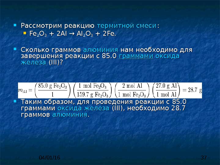
04/01/16 37 Рассмотрим реакцию термитной смеси : : Fe. Fe 22 OO 33 + 2 Al → Al 22 OO 33 + 2 Fe. Сколько граммов алюминия нам необходимо для завершения реакции с 85. 0 граммами оксида железа (III)? Таким образом, для проведения реакции с 85. 0 граммами оксида железа (III), необходимо 28. 7 граммов алюминия. .
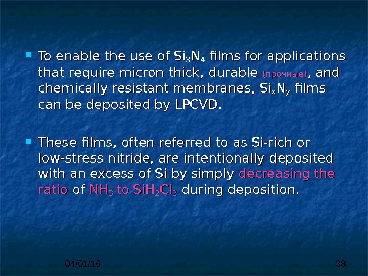
04/01/16 38 To enable the use of Si 33 NN 44 films for applications that require micron thick, durable (прочные) , and chemically resistant membranes, Si. Si xx NN yy films can be deposited by LPCVD. These films, often referred to as Si-rich or low-stress nitride, are intentionally deposited with an excess of Si by simply decreasing the ratio of of NHNH 3 3 to Si. H 22 Cl. Cl 22 during deposition.
04/01/16 39 Nearly stress-free films can be deposited using a NH 33 to Si. H 22 Cl. Cl 22 ratio of 1 : 6 , a deposition temperature of of 850 ◦◦ CC , and a pressure of 500 mtorr. The increase in Si content not only leads to a reduction in tensile stress, but also a decrease in the etch rate in HF. Such properties have enabled the development of fabrication techniques that would otherwise not be feasible with stoichiometric Si 33 NN 44. .
04/01/16 40 Germanium-Based Materials Like Si, Ge has a long history as a semiconductor device material, dating back to the development of the earliest transistors and semiconductor strain gauges. Issues related to the water solubility of germanium oxide , , however, stymied the development of Ge for microelectronic devices. Nonetheless, there is a renewed interest i i n using Ge in micromachined devices due to the relatively lowlow processing temperatures required to deposit the material.
04/01/16 41 Polycrystalline Ge Thin polycrystalline Ge (poly-Ge) films can be deposited by LPCVD at temperatures as low as 325 ◦◦ C on Si, Ge, and Si. Ge substrates. . Ge does not nucleate on Si. O 22 surfaces, which prohibits the use of thermal oxides and LTO films as sacrificial layers, but enables the use of these films as sacrificial molds. . Residual stress in poly-Ge films deposited on Si substrates can be reduced to nearly zero after short anneals at modest temperatures (30 s at 600 ◦◦ C).
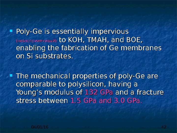
04/01/16 42 Poly-Ge is essentially impervious (невосприимчивый) to KOH, TMAH, and BOE, enabling the fabrication of Ge membranes on Si substrates. The mechanical properties of poly-Ge are comparable to polysilicon, having a Young’s modulus of 132 GPa and a fracture stress between 11. . 55 GPa and 3. . 00 GPa.
04/01/16 43 Mixtures of HNOHNO 33 , H, H 22 OO , and HCl andand HH 22 OO , , HH 22 OO 22 , , and HCl , as well as the RCA SC-1 cleaning solution isotropically etch Ge. Since these mixtures do not etch Si, Si. O 22 , Si 33 NN 44 , and Si. N, poly-Ge can be used as a a sacrificial substrate layer in polysilicon surface micromachining. RCA, the Radio Corporation ofof America
04/01/16 44 Werner Kern developed the basic procedure in 1965 while working for RCA, the Radio Corporation ofof America. . It involves the following: 1. 1. Removal of the organic contaminants (Organic Clean) 2. 2. Removal of thin oxide layer (Oxide Strip) 3. 3. Removal of ionic contamination (Ionic Clean)
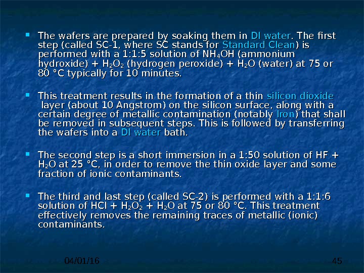
04/01/16 45 The wafers are prepared by soaking them in DI DI water. The first step (called SC-1, where SC stands for Standard Clean ) is performed with a 1: 1: 5 solution of NH 44 OH (ammonium hydroxide) + H 22 OO 22 (hydrogen peroxide) + H 22 O (water) at 75 or 80°C typically for 10 minutes. This treatment results in the formation of a thin silicon dioxide layer (about 10 Angstrom) on the silicon surface, along with a certain degree of metallic contamination (notably Iron ) that shall be removed in subsequent steps. This is followed by transferring the wafers into a DI DI water bath. The second step is a short immersion in a 1: 50 solution of HF + HH 22 O at 25°C, in order to remove the thin oxide layer and some fraction of ionic contaminants. The third and last step (called SC-2) is performed with a 1: 1: 6 solution of HCl + H 22 OO 22 + H+ H 22 O at 75 or 80°C. This treatment effectively removes the remaining traces of metallic (ionic) contaminants.
04/01/16 46 Using these techniques, devices such as poly-Ge-based thermistors and Si 33 NN 44 membrane-based pressure sensors, made using poly-Ge sacrificial layers, have been fabricated. Franke et al. found no performance degradation in Si CMOS devices following the fabrication of surface micromachined poly-Ge structures, thus demonstrating the potential for on-chip -integration of Ge electromechanical devices with Si circuitry.
04/01/16 47 Polycrystalline Si. Ge Like poly-Ge, polycrystalline Si. Ge (poly-Si. Ge) is a material that can be deposited at temperatures lower than those required for polysilicon. Deposition processes include LPCVD, APCVD, and RTCVD (rapid thermal CVD) using Si. H 44 and Ge. H 44 as precursor gases. Deposition temperatures range from 450 ◦◦ CC for LPCVD to to 625 ◦◦ CC by rapid thermal CVD (RTCVD).
04/01/16 48 In. In general, the deposition temperature is related to the concentration of Ge in the films, with higher Ge concentrations resulting in lower deposition temperatures. Быстродействующее термическое химическое парофазное осаждение (( англ. Rapid thermal CVD (RTCVD) )— CVD-процесс, использующий лампы накаливания или другие методы быстрого нагрева подложки. Нагрев подложки без разогрева газа позволяет сократить нежелательные реакции в газовой фазе.
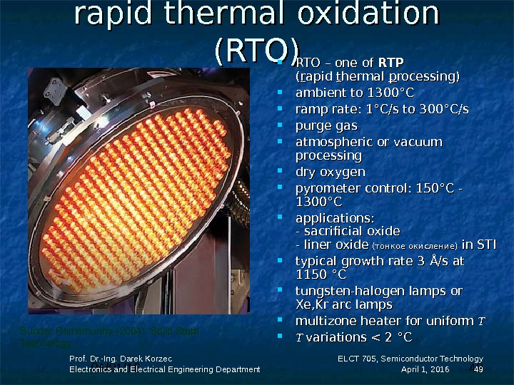
04/01/16 49 Prof. Dr. -Ing. Darek Korzec Electronics and Electrical Engineering Department ELCT 705, Semiconductor Technology April 1, 2016 49 rapid thermal oxidation (RTO) RTO – one of RTPRTP (( rr apid tt hermal pp rocessing) ambient to 1300 °° CC ramp rate: 1 °° C/s to 300 °° C/s purge gas atmospheric or vacuum processing dry oxygen pyrometer control: 150 °° C — 1300 °° CC applications: — sacrificial oxide — liner oxide (( тонкое окисление) in STI typical growth rate 3 ÅÅ /s at 1150 °° C C tungsten-halogen lamps or Xe, Kr arc lamps multizone heater for uniform T T variations < 2 °° C C Sundar Ramamurthy (2004). Solid State Technology
04/01/16 50 Like polysilicon, poly-Si. Ge can be doped with boron and phosphorus to modify its conductivity. In situ boron doping can be performed at temperatures as low as 450 ◦◦ C. C. Sedky et al. showed that the deposition temperature of conductive films doped with boron could be further reduced to 400 ◦◦ CC if if the Ge content was kept at or above 70%.
04/01/16 51 Unlike poly-Ge, poly-Si. Ge can be deposited onon a number of sacrificial substrates, including Si. O 22 , , PSG, and poly-Ge. For Ge rich films , , a a thin polysilicon seed layer is sometimes used on Si. O 22 surfaces since Ge. Ge does not readily nucleate on oxide surfaces. Like many compound materials, variations in in film composition can change the physical properties of the material.
04/01/16 52 For instance, etching of poly-Si. Ge by H 22 OO 22 becomes significant for Ge. Ge concentrations over 70%. Sedky et al. have shown that the microstructure, film conductivity, residual-stress, and residual stress gradient are related to the concentration of Ge in the material. With respect to residual stress, Franke et al. produced in situ boron doped films with residual compressive stresses as low as 10 MPa.
04/01/16 53 The poly-Si. Ge, poly-Ge material system is particularly attractive for surface micromachining since H 22 OO 22 can be used as a release agent. It has been reported that poly-Ge etches at a rate of 00. . 4 microns // min in HH 22 OO 22 , , while poly-Si. Ge with Ge concentrations below 80% have no observable etch rate after 40 hrs. The ability to use H 22 OO 22 as a sacrificial etchant makes the combination of poly-Si. Ge and poly-Ge extremely attractive for surface micromachining from the processing, safety, and materials compatibility points of view.
04/01/16 54 Due to the conformal nature of LPCVD processing, poly-Si. Ge structural elements, such as gimbal-based microactuator (микроактюатор с кардановым подвесом) structures, have been made by high-aspect ratio micromolding. (Интеграция с Si-ИС) Capitalizing on the low deposition temperatures, an integrated MEMS fabrication process with Si ICs has been demonstrated.
04/01/16 55 In this process, CMOS structures are first fabricated on Si wafers. Poly-Si. Ge mechanical structures are then surface micromachined using a poly-Ge sacrificial layer. (( Вертикальное расположение Si/Si. Ge/Poly-Ge technology) A significant advantage of this design is that the MEMS structure is positioned directly above the CMOS structure, thus reducing the parasitic capacitance and contact resistance characteristic of interconnects associated with side-by-side integration schemes.
04/01/16 56 Use of H 22 OO 2 2 as the sacrificial etchant means that no special protective layers are required to protect the underlying CMOS layer during release. In addition to its utility as a material for integrated MEMS devices, poly-Si. Ge has been identified as a material well suited for micromachined thermopiles (термоэлемент ы)ы) due to its lower thermal conductivity relative to Si.
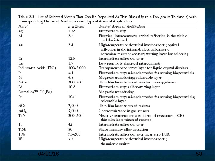
04/01/16 57 Metals M etallic thin films are used in many different capacities ranging from etch masks used in device fabrication to interconnects and structural elements in microsensors and microactuators. Metallic thin films can be deposited using a wide range of techniques, including evaporation, sputtering, CVD, and electroplating.
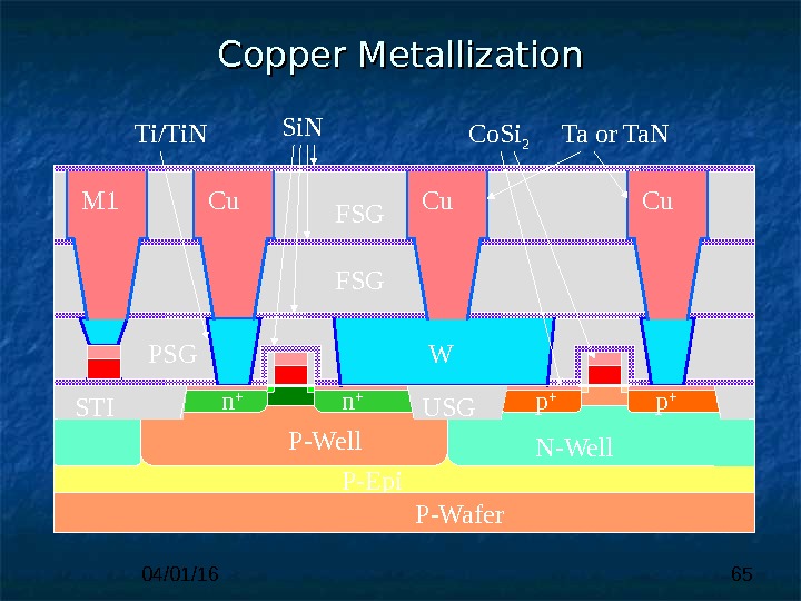
04/01/
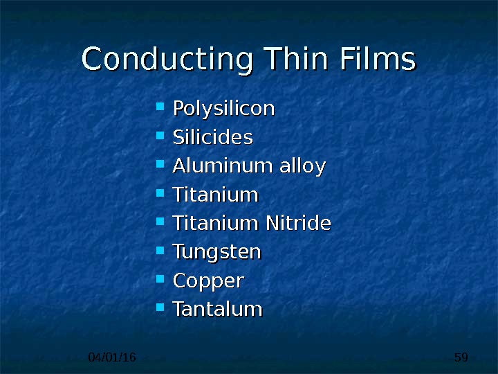
04/01/16 59 Polysilicon Silicides Aluminum alloy Titanium Nitride Tungsten Copper Tantalum Conducting Thin Films
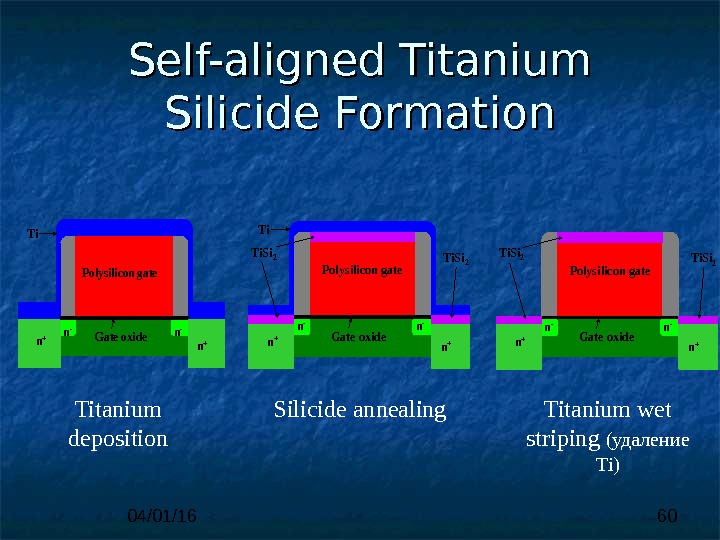
04/01/16 60 Polysilicon gate Gate oxiden-n- n+n+ Ti Polysilicon gate Gate oxide n-n- n+n+ Ti. Si 2 Titanium deposition Silicide annealing Titanium wet striping (удаление Ti)Self-aligned Titanium Silicide Formation
04/01/16 61 CMOS: Standard Metallization P-wafer N-Well. P-Well. STI n + USG p +Metal 1, Al • Cu BPSGW P-epi Ti. Si 2 Ti. N, ARCTi/Ti. N Anti-reflection coating (ARC)
04/01/16 62 Fluorosilicate glass (FSG) is a low-k dielectric used in between copper metal layers during silicon integrated circuit fabrication process. It has a low dielectric constant (k) and is now widely adopted by semiconductor foundries on geometries sub 0. 25μ. Fluorosilicate glass is effectively afluorine-containingsilicon dioxide(k=3. 5, while k of undoped silicon dioxide is 3. 9). Fluorosilicate glass is used by. IBM. Intelstarted using Cu metal layers and FSG on its 1. 2 GHz. Pentiumprocessor at 130 nm CMOS. .
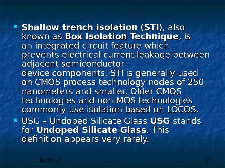
04/01/16 63 Shallow trench isolation (( STISTI ), also known as Box Isolation Technique , is anintegrated circuitfeature which preventselectrical currentleakagebetween adjacentsemiconductor devicecomponents. STI is generally used on. CMOSprocess technology nodes of 250 nanometersand smaller. Older CMOS technologies and non-MOS technologies commonly use isolation based on. LOCOS. USG – Undoped Silicate Glass USGUSG stands forfor Undoped Silicate Glass. This definition appears very rarely.
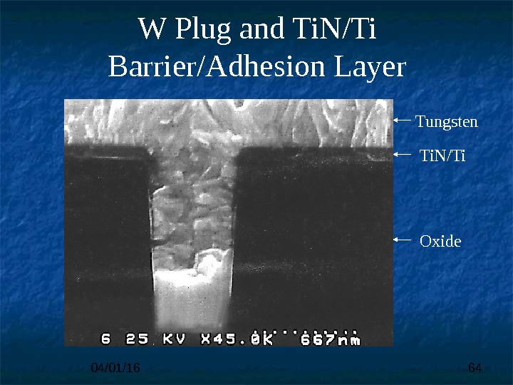
04/01/16 64 Tungsten Ti. N/Ti Oxide. W Plug and Ti. N/Ti Barrier/Adhesion Layer
04/01/16 65 P-Epi P-Wafer N-Well. P-Welln + STI p + USG WPSG WFSG n +M 1 Cu Co. Si 2 Ta or Ta. NTi/Ti. N Si. N Cu Cu FSGCopper Metallization
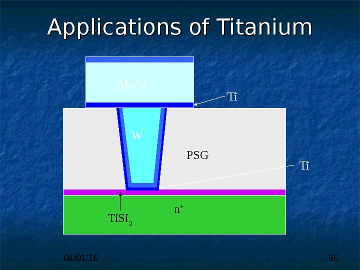
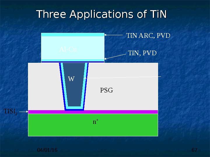
04/01/16 66 Applications of Titanium Ti PSG Ti. Si 2 n + Ti. WAl-Cu
04/01/16 67 PSG Ti. Si 2 n + Ti. N, PVD WAl-Cu Ti. N ARC, PVDThree Applications of Ti. N
04/01/16 68 Aluminum (Al) and gold (Au) are among the most widely employed metals in microfabricated electronic and MEM devices, as a result of their useas innerconnect and packaging materials. In addition to these critical electrical functions, Al and Au are also desirable as electromechanical materials.
04/01/16 69 One such example is the use of Au micromechanical switches for RF MEMS. For conventional RF applications, chip level switching is currently performed using FET (полевой транзистор)- and PIN diode-based solid state devices fabricated from gallium arsenide (Ga. As) substrates.
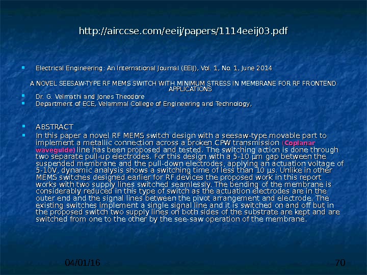
04/01/16 70 http: //airccse. com/eeij/papers/1114 eeij 03. pdf Electrical Engineering: An International Journal (EEIJ), Vol. 1, No. 1, June 2014 A NOVEL SEESAW-TYPE RF MEMS SWITCH WITH MINIMUM STRESS IN MEMBRANE FOR RF FRONTEND APPLICATIONS Dr. G. Velmathi and Jones Theodore Department of ECE, Velammal College of Engineering and Technology, ABSTRACT In this paper a novel RF MEMS switch design with a seesaw-type movable part to implement a metallic connection across a broken CPW transmission (( Coplanar waveguide )) line has been proposed and tested. The switching action is done through two separate pull-up electrodes. For this design with a 5 -10 µm gap between the suspended membrane and the pull-down electrodes, applying an actuation voltage of 5 -10 V, dynamic analysis shows a switching time of less than 10 µs. Unlike in other MEMS switches designed earlier for RF devices the proposed work in this report works with two supply lines switched seamlessly. The bending of the membrane is considerably reduced in this type of switch as the actuation electrodes are in the outer end and the signal lines between the pivot arrangement and electrode. The existing switches implement a single signal line and it is switched on and off but in the proposed switch two supply lines on both sides of the substrate are kept and are switched from one to the other by the see-saw operation of the membrane.
04/01/16 71 Unfortunately, these devices suffer ( страдают ) from insertion losses and poor electrical solation. In an effort to develop replacements for Ga. As-based solid state switches, Hyman et al. r eported the development of an electrostatically actuated, cantilever-based micromechanical switch fabricated on Ga. As substrates.
04/01/16 72 The trilayer cantilever structure was chosen to minimize the deleterious effects of thermal and process-related stress gradients in order to produce unbent (не разогнутые балки) and thermally stable beams. After deposition and pattering, the cantilevers were released in HF.
04/01/16 73 The processing steps proved to be completely compatible with Ga. As substrates. The released cantilevers demonstrated switching speeds better than 50µs at 25 V with contact lifetimes exceeding 109 cycles.
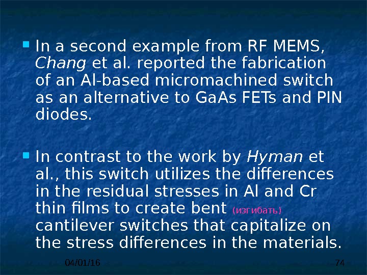
04/01/16 74 In a second example from RF MEMS, Chang et al. reported the fabrication of an Al-based micromachined switch as an alternative to Ga. As FETs and PIN diodes. In contrast to the work by Hyman et al. , this switch utilizes the differences in the residual stresses in Al and Cr thin films to create bent ( изгибать ) cantilever switches that capitalize on the stress differences in the materials.
04/01/16 75 Each switch is comprised of a series of linked bimorph cantilevers designed in such a way that the resulting structure bends significantly out of the plane of the wafer due to the stress differences in the bimorph. The switch is drawn closed by electrostatic attraction. The bimorph consists of metals that can easily be processed with Ga. As wafers, thus making integration with Ga. As devices possible.
04/01/16 76 The released switches were relatively slow, at 10 ms, but an actuation voltage of only 26 V was needed to close the switch. Thin-film metallic alloys that exhibit the shapememory effect are of particular interest to the MEMS community for their potential in microactuators. The shape-memory effect relies on the reversible transformation from a ductile (эластичный) martensite phase to a stiff (жесткий) austenite phase in the material with the application of heat.
04/01/16 77 The reversible phase change allows the shape-memory effec t to be used as an actuation mechanism, since the material changes shape during the transition. It has been found that high forces and strains can be generated from shape-memory thin films at reasonable power inputs, thus enabling shape-memory actuation to be used in MEMS-based microfluidic devices, such as microvalves and micropumps.
04/01/16 78 Titanium-nickel (Ti. Ni) is among the most popular of the shape-memory alloys, owing to its high actuation work density (50 MJ / m 3) and large bandwidth (up to 0. 1 k. Hz). Ti. Ni is also attractive because conventional sputtering techniques can be employed to deposit thin films, as detailed in a recent report by Shih et al.
04/01/16 79 In this study, Ti. Ni films were deposited by co-sputtering elemental Ti and Ni targets, and a co-sputtering Ti. Ni alloy and elemental Ti targets. It was reported that co-sputtering from Ti. Ni and Ti targets produced better films due to process variations related to the roughening of the Ni target in the case of Ti and Ni co-sputtering. The Ti. Ni/Ti co-sputtering process has been used to produce shape-memory material for a silicon spring-based microvalve.
04/01/16 80 Use of thin-film metal alloys in magnetic actuator systems is another example of the versatility of metallic materials in MEMS. Magnetic actuation in microdevices generally requires the magnetic layers to be relatively thick (tens to hundreds of microns) to generate magnetic fields of sufficient strength to generate the desired actuation. To this end, magnetic materials are often deposited by thick film methods , such as electroplating.