
03/31/16 11 Harsh Environment Semiconductors Silicon Carbide


3-_material_aspects_of_micro-_and_nanoelectromechanical_systems.ppt
- Размер: 1.2 Mегабайта
- Количество слайдов: 76
Описание презентации 03/31/16 11 Harsh Environment Semiconductors Silicon Carbide по слайдам
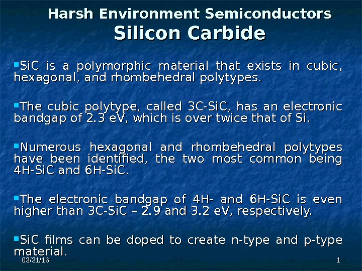
03/31/16 11 Harsh Environment Semiconductors Silicon Carbide Si. C is a polymorphic material that exists in cubic, hexagonal, and rhombehedral polytypes. The cubic polytype, called 3 C-Si. C, has an electronic bandgap of 2. . 3 e. V, which is over twice that of Si. Numerous hexagonal and rhombehedral polytypes have been identified, the two most common being 4 H-Si. C and 6 H-Si. C. The electronic bandgap of 4 H- and 6 H-Si. C is even higher than 3 C-Si. C – 2– 2. . 9 and 3. . 2 e. V, respectively. Si. C films can be doped to create n-type and p-type material.
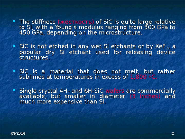
03/31/16 22 The stiffness (жесткость) of Si. C is quite large relative to Si, with a Young’s modulus ranging from 300 GPa to 450 GPa, depending on the microstructure. Si. C is not etched in any wet Si etchants or by Xe. F 22 , a popular dry Si etchant used for releasing device structures. Si. C is a material that does not melt, but rather sublimes at temperatures in excess of 11 , , 800 ◦C. Single crystal 4 H- and 6 H-Si. C wafers are commercially available, but smaller in diameter (3 inches) and much more expensive than Si.
03/31/16 33 Si. C thin films can be grown or deposited using a number of different techniques. For high-quality single crystal films, APCVD and LPCVD processes are most commonly employed. Homoepitaxial growth of 4 H- and 6 H-Si. C yields high quality films suitable for microelectronic applications, but only on substrates of the same polytype. These processes usually employ dual precursors , such as Si. H 4 and C 3 H 8 , and are performed at temperatures ranging from 1 , 500 ◦C to 1 , 700 ◦C.
03/31/16 44 Epitaxial films with p-type or n-type conductivity can be grown usin g aluminum and boron for p-type films and nitrogen and phosphorus for n-type films. Nitrogen is so effective at modifying the conductivity of Si. C that growth of undoped Si. C is extremely challenging (перспективный) , because the concentrations of residual nitrogen in typical deposition systems are sufficient for n-type doping.
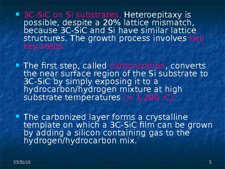
03/31/16 55 3 C-Si. C on Si substrates. Heteroepitaxy is possible, despite a 20% lattice mismatch, because 3 C-Si. C and Si have similar lattice structures. The growth process involves two key steps. The first step, called carbonization , converts the near surface region of the Si substrate to 3 C — Si. C by simply exposing it to a hydrocarbon/hydrogen mixture at high substrate temperatures ( > 1 , 200 ◦ C). The carbonized layer forms a crystalline template on which a 3 C-Si. C film can be grown by adding a silicon containing gas to the hydrogen/hydrocarbon mix.
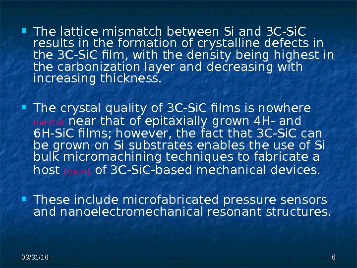
03/31/16 66 The lattice mismatch between Si and 3 C-Si. C results in the formation of crystalline defects in the 3 C-Si. C film, with the density being highest in the carbonization layer and decreasing with increasing thickness. The crystal quality of 3 C-Si. C films is nowhere ( ничто ) near that of epitaxially grown 4 H- and 6 H-Si. C films; however, the fact that 3 C-Si. C can be grown on Si substrates enables the use of Si bulk micromachining techniques to f abricate a host ( сонм ) of 3 C-Si. C-based mechanical devices. These include microfabricated pressure sensors and nanoelectromechanical resonant structures.
03/31/16 77 Polycrystalline Si. C (poly-Si. C) has proven to be a very versatile (универсальный) material for Si. C MEMS. Unlike (в отличие от) single crystal versions of Si. C, poly-Si. C can be deposited on a variety of substrate types, including such common surface micromachining materials as polysilicon, Si. O 2 , and Si 3 N 4 , using a much wider range of processes than epitaxial films.
03/31/16 88 Commonly used deposition techniques include LPCVD and APCVD. The deposition of poly-Si. C requires much lower substrate temperatures than epitaxial films, ranging from roughly 700 ◦ C to 1 , 200 ◦ C. Amorphous Si. C can be deposited at even lower temperatures (25 ◦ C to 400 ◦ C) by PECVD an d sputtering. The microstructure of poly-Si. C films is temperature, substrate, and process dependent.
03/31/16 99 For amorphous substrates, such as Si. O 2 and Si 3 N 4 , APCVD poly-Si. C films deposited from silane and propane are oriented randomly with equiaxed grains, whereas for oriented substrates, such as polysilicon, the texture of the poly-Si. C film matches that of the substrate. By comparison, poly-Si. C films deposited by LPCVD from dichlorosilane and acetylene are highly textured (111) films with a columnar microstructure, while films deposited from disilabutane have a distribution of orientations. This variation suggests that device performance can be tailored by selecting the proper substrate and deposition conditions.
03/31/16 1010 Direct bulk micromachining of Si. C is very difficult due to its chemical inertness. Although conventional wet chemical techniques are not effective, several electrochemical etch processes have been demonstrated and used in the fabrication of 6 H-Si. C pressure sensors. The etching processes are selective to the conductivity of the material , so dimensional control of the etched structures depends on the ability to form doped layers, which can only be formed by in situ or ion implantation processes, since solid source diffusion is not possible at reasonable processing temperatures. This constraint somewhat limits the geometrical complexity of the patterned structures, as compared with conventional plasma-based etching.
03/31/16 1111 To fabricate thick (hundreds of microns), 3 -D, high-aspect ratio Si. C structures, a molding technique has been developed. The molds are fabricated from Si substrates using deep reactive ion etching and then filled with Si. C using a combination of thin epitaxial and thick polycrystalline film CVD processes. The thin film process is used to protect the mold from pitting ( выщербление) during the more aggressive mold filling Si. C growth step.
03/31/16 1212 The mold filling process coats all surfaces of the mold with a Si. C film as thick as the mold is deep. To release the Si. C structure , the substrate is first mechanically polished to expose sections of the Si mold, then the substrate is immersed in a Si etchant to completely dissolve the mold. This process has been used to fabricate solid Si. C fuel atomizers (пульверизатор) , and a variant has been used to fabricate Si. C structures for micropower systems.
03/31/16 1313 In addition to CVD processes, bulk micromachined Si. C structures can be fabricated using sintered Si. C powders. Tanaka et al. describe a process in which Si. C components, such as micro gas turbine engine rotors, can be fabricated from Si. C powders using a micro-reaction — sintering process. The molds are microfabricated from Si using DRIE and filled with Si. C and graphite powders mixed with a phenol resin.
03/31/16 1414 The molds are then reaction-sintered using a hot isostatic pressing technique. The Si. C components are then released from the Si mold by wet chemical etching. The authors reported that the component shrinkage was less than 3%. The bending strength and Vickers hardness of the microreaction- sintered material was roughly 70 to 80% of commercially available reaction-sintered Si. C, the difference being attributed to the presence of unreacted Si in the micro-scale components.
03/31/16 1515 In a related process, Liew et al. detail a technique to create silicon carbon nitride (Si. CN) MEMS structures by molding injectable polymer precursors. Unlike the aforementioned processes, this technique uses SU-8 photoresists for the molds. SU-8 is a versatile photo-definable polymer in which thick films (hundreds of microns) can be patterned using conventional UV photolithographic techniques. After patterning, the molds are filled with the Si. CN-containing polymer precursor, lightly polished, and then subjected to a multistep heat-treating process. During thermal processing steps, the SU-8 mold decomposes, and the Si. CN structure is released. The resulting Si. CN structures retain ( сохраняет) many of the same properties of stoichiometric Si. C.
03/31/16 1616 Although Si. C cannot be etched using conventional wet etch techniques, thin Si. C films can be patterned using conventional dry etching techniques. RIE processes using fluorinated compounds, such as CHF 3 and SF 6 combined with O 2 , an inert gas, or H 2. The high oxygen content in these plasmas generally prohibits the use of photoresist as a masking material, therefore, hard masks made of Al, Ni, and ITO are often used.
03/31/16 1717 RIE-based Si. C surface micromachining processes with polysilicon and Si. O 2 sacrificial layers have been developed for single layer devices. Multilayered structures are very difficult to fabricate by direct RIE because the etch rates of the sacrificial layers are much higher than the Si. C structural layers, making critical dimensional control very difficult and RIE-based Si. C multilayer processes impractical. (Из-за высокой скорости травления жертвенных слоев трудно контролировать размеры структур, поэтому многослойные структуры на Si. C не используются).
03/31/16 1818 To address the issues related to RIE of multilayer Si. C structures, a micromolding process for patterning Si. C films on sacrificial layer substrates has been developed. (Как альтернатива используется микроформование). In essence (в сущности), the micromolding technique is the thin film analog to the molding-based, bulk micromachining technique presented earlier. The micromolding process utilizes polysilicon and Si. O 2 films as both molds and sacrificial substrate layers , with Si. O 2 molds used with polysilicon sacrificial layers and vica versa.
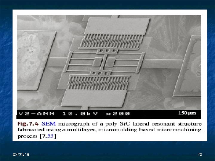
03/31/16 1919 These films are deposited and patterned using conventional methods, thus leveraging the well characterized and highly selective processes developed for polysilicon MEMS. Poly-Si. C films are simply deposited into the micromolds, and mechanical polishing is used to remove poly-Si. C from the top of the molds. Appropriate etchants are then used to dissolve the molds and sacrificial layers. The micromolding method utilizes the differences in chemical properties of the three materials in this system in a way that bypasses the difficulties associated with chemical etching of Si. C. This technique has been extended to multilayer processes that have been used to fabricate Si. C micromotors and the lateral resonant structure shown in Fig. 7. 4.
03/31/
03/31/16 2121 Yang et al. have recently shown that the chemical inertness of Si. C facilitates the fabrication of NEMS devices. In this work, the authors present a fabrication method to realize Si. C mechanical resonators with submicron thickness and width dimensions. The resonators were fabricated from 260 nm-thick 3 C-Si. C films epitaxially grown on (100) Si wafers. The films were patterned into 150 nm-wide beams ranging in length from 2 to 8µm.
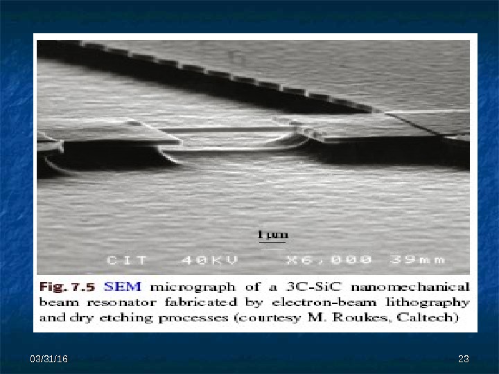
03/31/16 2222 The beams were etched in a NF 3 /O 2 /Ar plasma using an evaporated Cr etch mask. After patterning, the beams were released by etching isotropically the underlying Si using a NF 3 /Ar plasma. The inertness of the Si. C film to the Si etchant enables the dry release of the nanomechanical beams. An example of a 3 C-Si. C nanomechanical beam is shown in Fig. 7. 5.
03/31/
03/31/16 2424 Diamond is commonly known as nature’s hardest material, making it ideal for high wear environments. Diamond has a very large electronic bandgap (5. 5 e. V), which makes it attractive for high temperature electronics. Undoped diamond is a high quality insulator with a dielectric constant of 5. 5 ; however it can be relatively easily doped with boron to create p-type conductivity. Diamond has a very high Young’s modulus (1 , 035 GPa), making it suitable for high frequency micromachined resonators, and it is among nature’s most chemically inert materials, making it well suited for harsh chemical environments.
03/31/16 2525 Unlike Si. C, fabrication of diamond MEMS is currently restricted to polycrystalline and amorphous material, since epitaxial-quality single-crystal diamond wafers are not yet commercially available. (Растут поли и аморфные пленки, монокристаллических wafer нет) Polycrystalline diamond films can be deposited on Si and Si. O 2 substrates, but the surfaces often must be seeded by diamond powders , or biased with a negative charge to initiate growth.
03/31/16 2626 In general, diamond nucleates much more readily (охотнo ) o n Si surfaces than on Si. O 2 surfaces, an effect that has been used to selectively pattern diamond films into micromachined AFM cantilever probes using Si. O 2 molding masks. Bulk micromachining of diamond is very difficult given its extreme chemical inertness. Diamond structures have nevertheless been fabricated using bulk micromachined Si molds to pattern the structures. The Si molds were fabricated using conventional micromachining techniques and filled with polycrystalline diamond deposited by hot filament chemical vapor deposition (HFCVD).
03/31/16 2727 The HFCVD process uses hydrogen as a carrier gas and methane as the carbon source. The process was performed at a substrate temperature of 850 ◦ C to 900 ◦ C and a pressure of 50 mtorr. The Si substrate was seeded prior to deposition using a diamond particle/ ethanol solution.
03/31/16 2828 After deposition, the top surface of the structure was polished using a hot iron plate. After polishing, the Si mold was removed in a Si etchant, leaving behind the micromachined diamond structure. This process was used to produce high-aspect-ratio capillary channels for microfluidic applications and components for diffractive optics, laser-to-fiber alignment, and power device cooling structures.
03/31/16 2929 Due to the nucleation processes associated with diamond film growth, surface micromachining of polycrystalline diamond thin films requires modifications to conventional micromachining to facilitate film growth on sacrificial substrates. Conventional RIE methods are generally ineffective, so initial work focused on developing selective deposition techniques. One early method used selective seeding to form patterned templates for diamond nucleation.
03/31/16 3030 The selective seeding process employed the lithographic patterning of photoresist that contained diamond powders. The diamond-loaded photoresist was deposited and patterned onto a Cr-coated Si wafer. During the onset of diamond growth, the patterned photoresist rapidly evaporates, leaving behind the diamond seed particles in the desired locations. A patterned diamond film is then selectively grown on these locations.
03/31/16 3131 A second process utilizes selective deposition directly on sacrificial substrate layers. This process combines conventional diamond seeding with photolithographic patterning and etching to fabricate micromachined diamond structures on Si. O 2 sacrificial layers.
03/31/16 3232 The process can be performed in one of two ways. The first approach begins with the seeding of an oxidized Si wafer. The wafer is coated with photoresist and photolithographically patterned. Unmasked regions of the seeded Si. O 2 film are then partially etched, forming a surface unfavorable for diamond growth. The photoresist is then removed, and a diamond film is deposited on the seeded regions.
03/31/16 3333 The second approach also begins with an oxidized Si wafer. The wafer is coated with photoresist, photolithographically patterned, and then seeded with diamond particles. The photoresist is removed, leaving behind a patterned seed layer suitable for selective growth. These techniques have been successfully used to fabricate cantilever beams and bridge structures.
03/31/16 3434 A third method to surface micromachine polycrystalline diamond films follows the conventional approach of film deposition, dry etching, and release. The chemical inertness of diamond renders ( делает) most conventional plasma chemistries useless (бесполезный); however, oxygen-based ion beam plasmas can be used to etch diamond thin films. A simple surface micromachining process begins with the deposition of a polysilicon sacrificial layer on a Si 3 N 4 -coated Si wafer.
03/31/16 3535 The polysilicon layer is seeded using diamond slurry, and a diamond film is deposited by HFCVD. Since photoresist is not resistant to O 2 plasmas, an Al masking film is deposited and patterned. The diamond films are then etched in the O 2 ion beam plasma, and the structures are released by etching the polysilicon with KOH. This process has been used to create lateral resonant structures, but a significant stress gradient in the films rendered the devices nonoperational.
03/31/16 3636 In general, conventional HFCVD requires that the substrate be pretreated with a seeding layer prior to diamond film growth. However, a method called biased enhanced nucleation (BEN) has been developed that enables the growth of diamond on unseeded Si surfaces. Wang et al. have shown that if Si substrates are masked with patterned Si. O 2 films, selective diamond growth will occur primarily on the exposed Si surfaces, and a slight HF etch is sufficient to remove the adventitious ( непредусмотренный ) diamond from the Si. O 2 mask. This group was able to use this method to fabricate diamond micromotor rotors and stators on Si surfaces.
03/31/16 3737 Diamond is a difficult but not impossible material to etch using RIE techniques. It is well-known that diamond will be etched in oxygen plasmas, but these plasmas are not generally well suited for device fabrication, because the etches tend to be isotropic. A recent development, however, suggests that RIE processes for diamond are close at hand ( под рукой ).
03/31/16 3838 Wang et al. describe a process to fabricate a vertically actuated, doubly clamped micromechanical diamond beam resonator using RIE. The process outlined here addresses two key issues related to diamond surface micromachining, namely, residual stress gradients in the diamond films and diamond patterning techniques. A microwave plasma CVD reactor was used to grow the diamond films on sacrificial Si. O 2 layers pretreated with a nanocrystalline diamond powder , resulting in a uniform nucleation density at the diamond/Si. O 2 interface.
03/31/16 3939 The diamond films were etched in a CF 4 /O 2 plasma using Al as a hard mask. Reasonably straight sidewalls were created, with roughness attributable to the surface roughness of the faceted diamond film. An Au/Cr drive electrode beneath the sacrificial oxide remained covered throughout the diamond patterning steps and, thus, was undamaged during the diamond etching process.
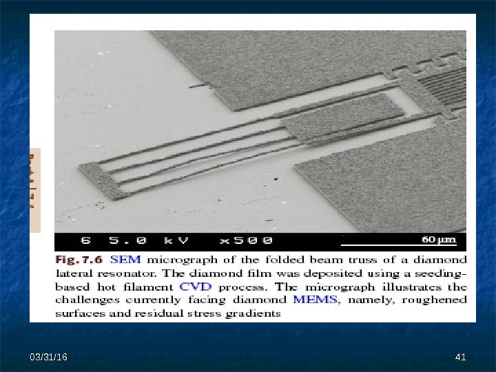
03/31/16 4040 In conjunction with recent advances in RIE and micromachining techniques, work is being performed to develop diamond deposition processes specifically for MEMS applications. Diamond films grown using conventional techniques, especially processes that require pre-growth seeding, tend to have high residual stress gradients and roughened surface morphologies as a result of the highly faceted, large grain polycrystalline films that are produced by these methods (see Fig. 7. 6). The rough surface morphology degrades the patterning process, resulting in roughened sidewalls in etched structures and roughened surfaces of films deposited over these layers.
03/31/
03/31/16 4242 Unlike polysilicon and Si. C, a post-deposition polishing process is not technically feasible for diamond due to its extreme hardness. For the fabrication of multilayer diamond devices, methods to reduce the surface roughness of the as-deposited films are highly desirable. Along these lines, Krauss et al. reported the development of an ultrananocrystalline diamond film that exhibits a much smoother surface morphology than comparable diamond films grown using conventional methods. Unlike conventional CVD diamond films that are grown using a mixture of H 2 and CH 4 , the ultrananocrystalline diamond films are grown from mixtures of Ar, H 2 , and C 60 or Ar, H 2 , and CH 4. Although the processes are still under development, Krauss et al. have demonstrated the viability of the ultrananocrystalline diamond films as conformal coatings on Si surfaces, as well as their utility in several micromachining processes.
03/31/16 4343 Ga. As, In. P, and Related III-V Materials Gallium Arsenide (Ga. As), Indium Phosphide (In. P), and related III-V compounds have favorable piezoelectric and optoelectric properties, high piezoresistive constants, and wide electronic bandgaps relative to Si, making them attractive for various sensor and optoelectronic applications. Like Si, significant research in bulk crystal growth has led to the development of Ga. As and In. P substrates, which are commercially available as high quality, single crystal wafers.
03/31/16 4444 Unlike compound semiconductors, such as Si. C, III-V materials can be deposited as ternary (тройной) and quaternary (четверной) alloys with lattice constants that closely match the binary compounds from which they are derived (i. e. , Al x Ga 1− x As and Ga. As), thus permitting the fabrication of a wide variety of heterostructures that facilitate device performance.
03/31/16 4545 Crystalline Ga. As has a zinc blend crystal structure with an electronic bandgap of 1. 4 e. V, enabling Ga. As electronic devices to function at temperatures as high as 350 ◦C. High quality, single crystal wafers are commercially available, as are well developed metalorganic chemical vapor deposition (MOCVD) and molecular beam epitaxy (MBE ) growth processes for epitaxial layers of Ga. As and its alloys. Ga. As does not outperform (не превосходит) Si in terms of mechanical properties, however, its stiffness and fracture toughness are still suitable for micromechanical devices.
03/31/16 4646 Micromachining of Ga. As is relatively straightforward ( простой ) , since many of its lattice-matched ternary and quaternary alloys have sufficiently different chemical properties to allow their use as sacrificial layers. For example, the most common ternary alloy for Ga. As is Al x Ga 1− x As. For values of x less than or equal to 0. 5, etchants containing mixtures of HF and H 2 O will etch Al x Ga 1− x As without attacking Ga. As , while etchants containing NH 4 OH and H 2 O 2 attack Ga. As isotropically, but do not etch Al x Ga 1− x As. Such selectivity enables the micromachining of Ga. As wafers using lattice-matched etch stops and sacrificial layers.
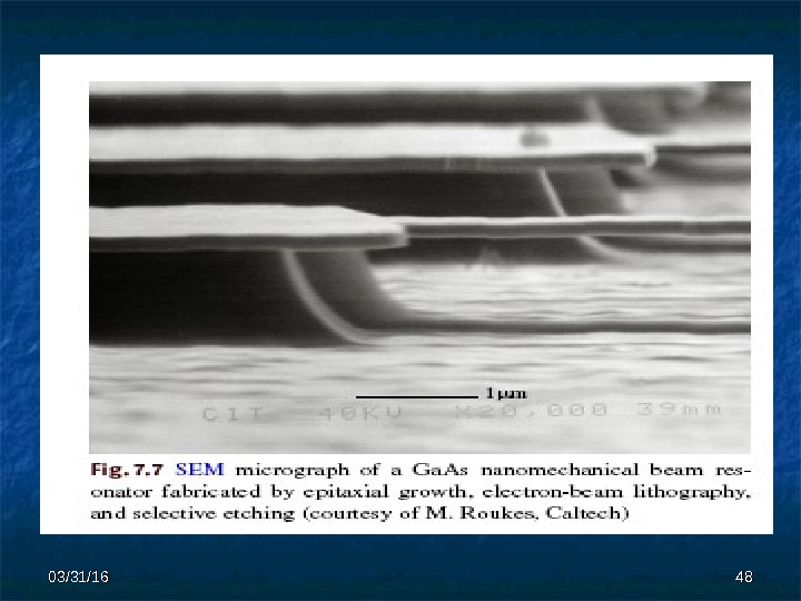
03/31/16 4747 Devices fabricated using these methods include comb drive lateral resonant structures, pressure sensors , thermopile sensors, Fabry–Perot detectors, and cantilever-based sensors and actuators. In addition, nanoelectromechanical devices, such as suspended micromechanical resonators and tethered membranes, have been fabricated using these techniques. An example of a nanoelectromechanical beam structure fabricated from Ga. As is shown in Fig. 7. 7.
03/31/
03/31/16 4949 In addition to using epitaxial layers as etch stops, ion implantation methods can also be used to produce etch stops in Ga. As layers. Miao et al. d escribe a process that uses electrochemical etching to selectively remove n-type Ga. As layers. The process relies on the creation of a highly resistive near surface Ga. As layer on an n-type Ga. As substrate by low dose nitrogen implantation in the Me. V energy range. A pulsed electrochemical etch method using a H 2 Pt. Cl 6 , H 3 PO 4 , H 2 SO 4 platinum electrolytic solution at 40 ◦C with 17 V, 100 ms pulses is sufficient to selectively remove n-type Ga. As at about 3µm / min. Using this method, stress-free, tethered membranes could readily be fabricated from the high resistive Ga. As layer. The high implant energies enable the fabrication of membranes several microns in thickness.
03/31/16 5050 Moreover, the authors demonstrated that if the Ga. As wafer were etched in such a way as to create an undulating (волнистая поверхность) surface prior to ion implantation, corrugated membranes (гофрированная мембрана) could be fabricated. These structures can sustain (выдерживать) much higher deflection amplitudes than flat structures.
03/31/16 5151 Micromachining of In. P closely resembles the techniques used for Ga. As. Many of the properties of In. P are similar to Ga. As in terms of crystal structure, mechanical stiffness, and hardness. However, the optical properties of In. P make it particularly attractive for micro-optomechanical devices to be used in the 1. 3 to 1. 55µm wavelength range. Like Ga. As, single crystal wafers of In. P are readily available, and ternary and quaternary lattice-matched alloys, such as In. Ga. As, In. Al. As, In. Ga. As. P, and In. Ga. Al. As , can be used as either etch stop and/or sacrificial layers, depending on the etch chemistry.
03/31/16 5252 For instance, In. P structural layers deposited on In 0. 53 Al 0. 47 As sacrificial layers can be released using etchants containing C 6 H 8 O 7 , H 2 O 2 , and H 2 O. Citric acid is a weak organic acid with the formula C 6 H 8 O 7. In addition, In. P films and substrates can be etched in solutions containing HCl and H 2 O using In 0. 53 Ga 0. 47 As films as etch stops. Using In. P-based micromachining techniques, multi-air gap filters, bridge structures, and torsiona l membranes have been fabricated from In. P and its related alloys.
03/31/16 5353 In addition to Ga. As and In. P, materials such as indium arsenide (In. As) can be micromachined into device structures. Despite a 7% lattice mismatch between In. As and (111) Ga. As, high quality epitaxial layers can be grown on Ga. As substrates. As described by Yamaguchi et al. , the surface Fermi level of In. As/Ga. As structures is pinned (находится или близок) in the conduction band, enabling the fabrication of very thin conductive membranes.
03/31/16 5454 In fact, the authors have successfully fabricated freestanding In. As structures that range in thickness from 30 to 300 nm. The thin In. As films were grown directly on Ga. As substrates by MBE and etched using a solution containing H 2 O, H 2 O 2 , and H 2 SO 4. The structures, mainly doubly clamped cantilevers, were released by etching the Ga. As substrate using a H 2 O/H 2 O 2 /NH 4 OH solution.
03/31/16 5555 Piezo electric Materials Piezoelectric materials play an important role in MEMS technology for sensing and mechanical actuation applications. In a piezoelectric material, mechanical stress produces a polarization, and, conversely, a voltage induced polarization produces a mechanical stress. Many asymmetric materials, such as quartz, Ga. As, and zinc oxide (Zn. O), exhibit some piezoelectric behavior.
03/31/16 5656 Recent work in MEMS has focussed on the development of ferroelectric compounds, such as lead zirconate titanate, Pb(Zr x Ti 1−x ) O 3 , or PZT , because such compounds have high piezoelectric constants that result in high mechanical transduction. It is relatively straightforward ( простой ) to fabricate a PZT structure on top of a thin freestanding structural layer (i. e. , cantilever, diaphragm).
03/31/16 5757 Such a capability enables the piezoelectric material to be used in sensor applications or actuator applications for which piezoelectric materials are particularly well suited. Like Si, PZT films can be patterned using dry etch techniques based on chlorine chemistries, such as Cl 2 /CCl 4 , as well as ion beam milling using inert gases like Ar.
03/31/16 5858 PZT has been successfully deposited in thin film form using co-sputtering, CVD, and sol-gel processing. Sol-gel processing is particularly attractive because the composition and homogeneity of the deposited material over large surface areas can be readily controlled. The sol-gel process outlined by Lee et al. uses PZT solutions made from liquid precursors containing Pb, Ti, Zr, and O. The solution is deposited by spin coating on a Si wafer that has been coated with a P t /Ti/Si. O 2 thin film multilayer.
03/31/16 5959 The process is executed to produce a PZT film in layers, with each layer consisting of a spin-coated layer that is dried at 110 ◦C for 5 min and then heat treated at 600 ◦C for 20 min. After building up the PZT layer to the desired thickness, the multilayer was heated at 600 ◦C for up to 6 hrs. Prior to this anneal, a Pb. O top layer was deposited on the PZT surface. An Au/Cr electrode was then sputter deposited on the surface of the piezoelectric stack. This process was used to fabricate a PZT-based force sensor.
03/31/16 6060 Xu et al. describe a similar sol-gel process to produce 12µm-thick, crack-free PZT films on Pt-coated Si wafers and 5µm-thick films on insulating Zr. O 2 layers to produce micromachined MHz-range, two-dimensional transducer arrays for acoustic imaging.
03/31/16 6161 Thick film printing techniques for PZT have been developed to produce thick films in excess of 100µm. Such thicknesses are desired for applications that require actuation forces that cannot be achieved with the much thinner sol-gel films. Beeby et al. describe a thick film printing process whereby a PZT paste is made from a mixture of 95% PZT powder, 5% lead borosilicate powder, and an organic carrier. The paste was then printed through a stainless steel screen using a thick film printer.
03/31/16 6262 Printing was performed on an oxidized Si substrate that is capped with a Pt electrode. After printing, the paste was dried and then fired at 850 ◦C to 950 ◦C. Printing could be repeated to achieve the desired thickness. The top electrode consisted of an evaporated Al film. The authors found that it was possible to perform plasma-based processing on the printed substrates, but that the porous nature of the printed PZT films made them unsuitable for wet chemical processing.
03/31/16 6363 Polymer Materials Polyimides comprise an important class of durable polymers that are well suited for many of the techniques used in conventional MEMS processing. In general, polyimides can be acquired in bulk, or deposited as thin films by spin coating. Polyimides can be patterned using conventional dry etching techniques and processed at relatively high temperatures. These attributes make polyimides an attractive group of polymers for MEMS that require polymer structural and/or substrate layers, such as microfabricated biomedical devices, for which inertness and flexibility are important parameters.
03/31/16 6464 Polyimide Shearwood et al. explored the use of polyimide as a robust mechanical material for microfabricated audio membranes. The authors fabricated 7µm-thick, 8 mm-diameter membranes on Ga. As substrates by bulk micromachining the Ga. As substrate using a NH 3 /H 2 O 2 solution. They realized 100% yield and, despite a low Young’s modulus ( 3 GPa), observed flat membranes to within 1 nm ? after fabrication.
03/31/16 6565 Jiang et al. capitalized on the strength and flexibility of polyimide to fabricate a flexible she a r — stress ( касательных напряжений ) sensor array based on Si sensors. The sensor array consisted of a collection of Si islands linked by two polyimide layers. Each Si sensor island was 250 x 250µm 2 in area and 80µm in thickness. Al was used as an electrical innerconnect layer.
03/31/16 6666 The two polyimide layers served as highly flexible hinges (шарниры), giving the sensor array the ability to be mounted on curved surfaces. The sensor array was successful in profiling the shear-stress distribution along the leading edge of a rounded delta wing.
03/31/16 6767 The chemical and temperature durability of polyimides enables their use as a sacrificial layer for a number of commonly used materials, such as evaporated or sputter-deposited metals. Memmi et al. Developed a fabrication process for capacitive micromechanical ultransonic transducers using polyimide as a sacrificial layer. The authors showed that the polyimide could with stand the conditions used to deposit silicon monoxide by evaporation and silicon nitride by PECVD at 400 ◦C. Recent work by Bagolini et al. has shown that polyimides can even be used as sacrificial layers for PECVD Si. C.
03/31/16 6868 In the area of microfabricated biomedical devices, polyimide is receiving attention as a substrate material for implantable devices, owing to its potential biocompatiblity and mechanical flexibility. Stieglitz reported on the fabrication of multichannel microelectrodes on polyimide substrates. Instead of using polyimide sheets as starting substrates, Si carrier wafers coated with a 5µm-thick polyimide film were used. Pt microelectrodes were then fabricated on these substrates using conventional techniques. Thin polyimide layers were deposited between various metal layers to serve as insulating layers.
03/31/16 6969 A capping polyimide layer was then deposited on the top of the substrates, and the entire polyimide/metal structure was peeled off the Si carrier wafers. Backside processing was then performed on the freestanding polyimide structures to create devices that have exposed electrodes on both surfaces. In a later paper, Stieglitz et al. describe a variation of this process for neural prostheses.
03/31/16 7070 SU-8 is a negative-tone, epoxy-like photoresist that is receiving much attention for its versatility in MEMS processing. It is a high-aspect-ratio, UV-sensitive resistdesigned for applications requiring single-coat resists with thicknesses on the order of 500 microns. SU-8 has favorable chemical properties that enable it to be used as a molding material for high-aspect-ratio electroplated structures (as an alternative to LIGA), and as a structural material for microfluidics. In terms of mechanical properties, Lorenz et al. Reported that SU-8 has a modulus of elasticity of 4. 02 GPa, which compares favorably with a commonly used polyamid (3. 4 GPa).
03/31/16 7171 In addition to the aforementioned conventional uses for SU-8, several interesting alternative uses are beginning to appear in the literature. Conradie et al. have used SU-8 to trim the mass of silicon paddle oscillators as a means to adjust the resonant frequency of the beams. The trimming process involves the patterning of SU-8 posts on Si paddles (пластинк и) . The process capitalizes on the relative chemical stability of the SU-8 resin, in conjunction with the relatively large masses that can be patterned using standard UV exposure processes.
03/31/16 7272 SU-8 is also of interest as a bonding layermaterial for wafer bonding processes using patterned bonding layers. Pan et al. compared several UV photo-definable polymeric materials and found that SU-8 exhibited the highest bonding strength (20. 6 MPa) for layer thicknesses up to 100µm.
03/31/16 7373 Parylene (poly-para-xylylene) is another emerging polymeric MEMS material due in large part to its biocompatibility. It is particularly attractive from the fabrication perspective, because it can be deposited by CVD at room temperature.
03/31/16 7474 Moreover, the deposition process is conformal, which enables parylene coatings to be applied to prefabricated structures, such as Si microneedles, low stress silicon nitride membrane particle filters , and micromachined polyimide/Au optical scanners. In the first two cases, the parylene coating served to strengthen the microfabricated structures , while in the last case, it served to protect the structure from condensing water vapor.
03/31/16 7575 In addition to its function as a protective coating, parylene can actually be micromachined into freestanding components. Noh et al. Demonstrated a method to create bulk micromachined parylene microcolumns for miniature gas chromatographs. The structure is fabricated using a micromolding technique by which Si molds are fabricated by DRIE and coated with parylene to form three sides of the microcolumn. A second wafer is coated with parylene, and the two are bonded together via a fusion bonding process. After bonding, the structure is released from the Si mold by KOH etching. In a second example, Yao et al. describe a dry release process for parylene surface micromachining.
03/31/16 7676 In this process, sputtered Si is used as a sacrificial layer onto which a thick sacrificial photoresist is deposited. Parylene is then deposited on the photoresist and patterned into the desired structural shape. The release procedure is a two step process. First, the photoresist is dissolved in acetone. This results in the parylene structure sticking to the sputtered Si. Next, a dry Br. F 3 etch is performed, which dissolves the Si and releases the parylene structures. Parylene beams that were 1 mm long and 4. 5µm thick were successfully fabricated using this technique.