ab9df3b112fc9a8e65e4bc4373cd4072.ppt
- Количество слайдов: 44

表面波プラズマの トムソン散乱診断と 電子加熱機構 河野明廣 名古屋大学 学研究科 電子情報システム専攻 プラズマ科学のフロンティア 2008
Outline ・Motivation: electron heating mechanism in SWP ・Laser Thomson scattering measurement system ・Measurements for low-pressure SWP ・Fluid-Monte-Carlo hybrid modeling ・Conclusions
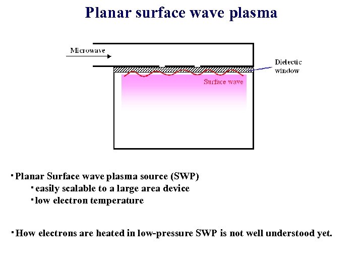
Planar surface wave plasma ・Planar Surface wave plasma source (SWP) ・easily scalable to a large area device ・low electron temperature ・How electrons are heated in low-pressure SWP is not well understood yet.
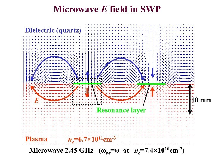
Microwave E field in SWP Dielectric (quartz) 10 mm E Resonance layer Plasma ne=6. 7× 1011 cm-3 Microwave 2. 45 GHz (wpe=w at nc=7. 4× 1010 cm-3)
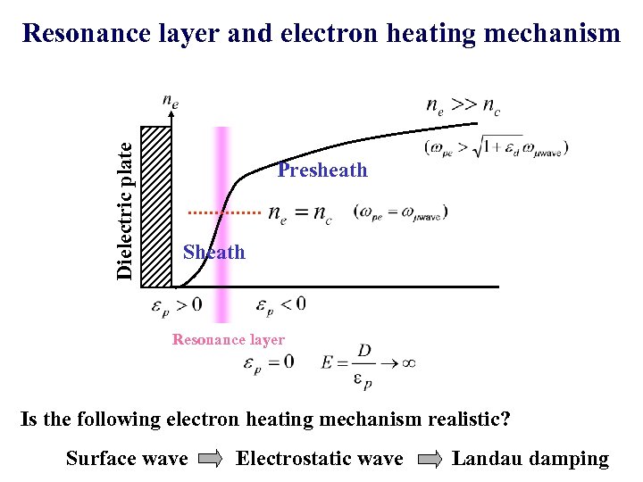
Dielectric plate Resonance layer and electron heating mechanism Presheath Sheath Resonance layer Is the following electron heating mechanism realistic? Surface wave Electrostatic wave Landau damping
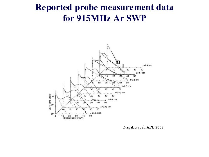
Reported probe measurement data for 915 MHz Ar SWP Nagatsu et al. APL 2002
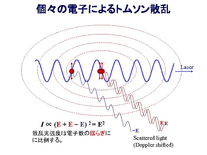
個々の電子によるトムソン散乱 Laser I ∝ E 2 + E)- E)4 E 2 (E E 2 = 散乱光強度は電子数の揺らぎに に比例する。 EE -E Scattered light (Doppler shifted)
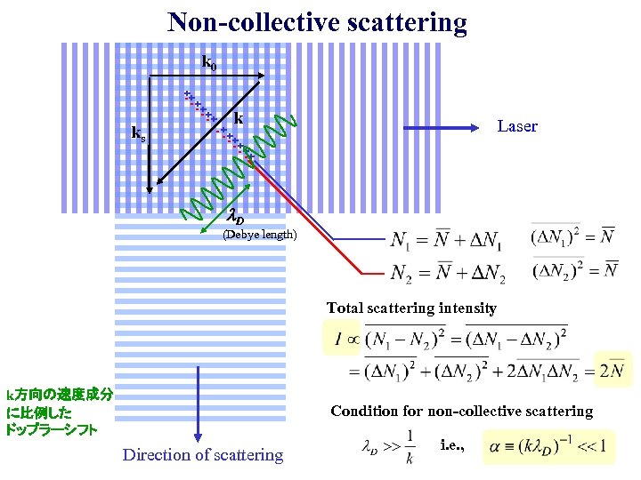
Non-collective scattering k 0 ks ++ -+ -+ - ++ --+ - ++ - -+ k Laser l. D (Debye length) Total scattering intensity k方向の速度成分 に比例した ドップラーシフト Condition for non-collective scattering Direction of scattering i. e. ,
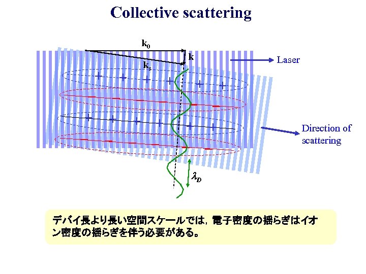
Collective scattering k 0 ks k + + + - - - - - Laser Direction of scattering l. D デバイ長より長い空間スケールでは,電子密度の揺らぎはイオ ン密度の揺らぎを伴う必要がある。
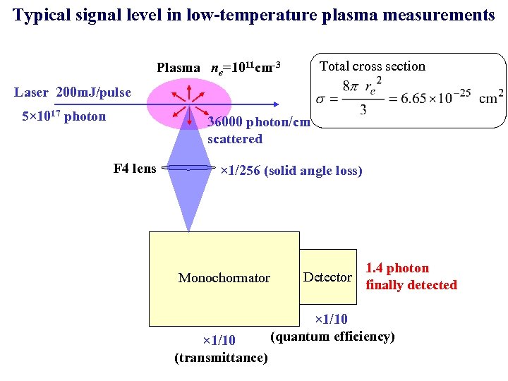
Typical signal level in low-temperature plasma measurements Total cross section Plasma ne=1011 cm-3 Laser 200 m. J/pulse 5× 10¹⁷ photon 36000 photon/cm scattered F 4 lens × 1/256 (solid angle loss) Monochormator × 1/10 (transmittance) Detector 1. 4 photon finally detected × 1/10 (quantum efficiency)
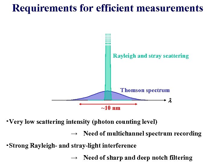
Requirements for efficient measurements Rayleigh and stray scattering Thomson spectrum l ~10 nm ・Very low scattering intensity (photon counting level) → Need of multichannel spectrum recording ・Strong Rayleigh- and stray-light interference → Need of sharp and deep notch filtering
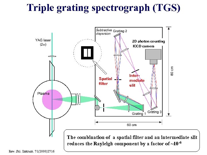
Triple grating spectrograph (TGS) 2 D photon counting ICCD camera Spatial filter Intermediate slit The combination of a spatial filter and an intermediate slit reduces the Rayleigh component by a factor of ~10 -6 Rev. Sci. Instrum. 71(2000)2716

Stray light elimination by TGS Entrance slit Intermediate slit Stray Thomson (Subtractive dispersion) 1 st grating 2 nd grating 3 rd grating Spatial filter Rayleigh Stray Thomson
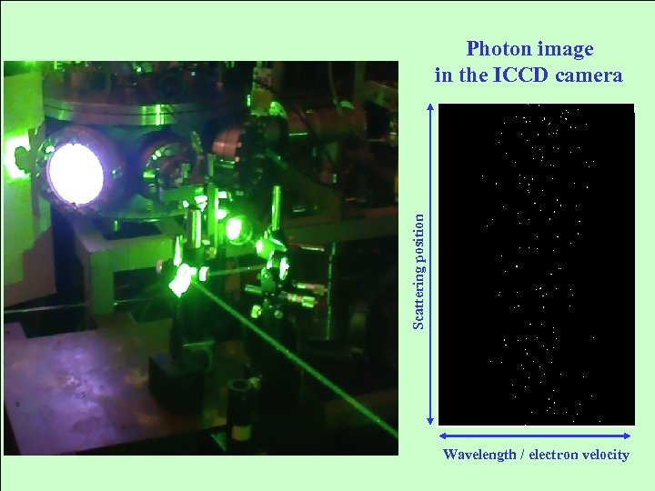
Scattering position Photon image in the ICCD camera Wavelength / electron velocity
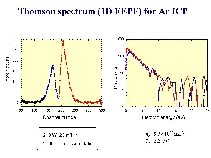
Thomson spectrum (1 D EEPF) for Ar ICP 1000 300 100 200 Photon count 250 100 50 10 1 0 50 100 150 200 250 300 350 0. 1 0 5 10 15 Channel number Electron energy (e. V) 200 W, 20 m. Torr ne=5. 5× 1011 cm-3 Te=2. 3 e. V 20000 shot accumulation 20 25
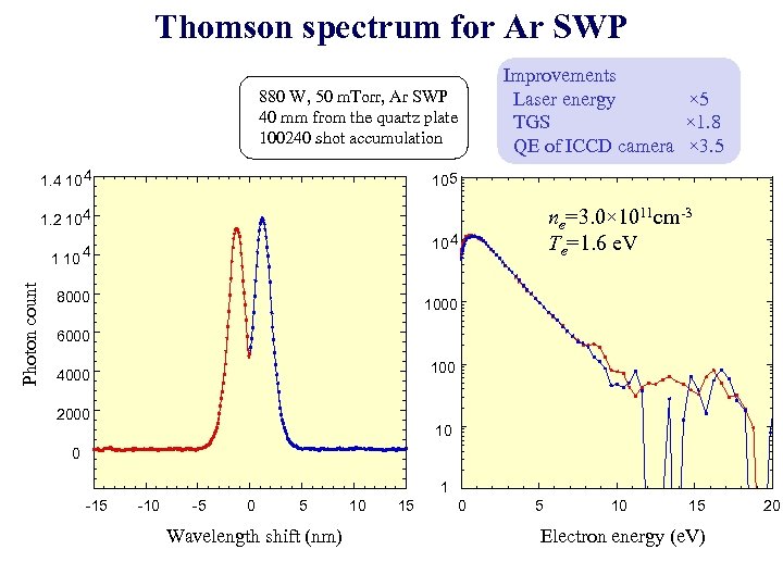
Thomson spectrum for Ar SWP 880 W, 50 m. Torr, Ar SWP 40 mm from the quartz plate 100240 shot accumulation 1. 4 10 4 Improvements Laser energy × 5 TGS × 1. 8 QE of ICCD camera × 3. 5 105 ne=3. 0× 1011 cm-3 Te=1. 6 e. V 1. 2 104 10 4 Photon count 1 10 4 8000 1000 6000 100 4000 2000 10 0 1 -15 -10 -5 0 5 Wavelength shift (nm) 10 15 0 5 10 15 Electron energy (e. V) 20
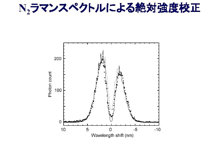
N 2ラマンスペクトルによる絶対強度校正
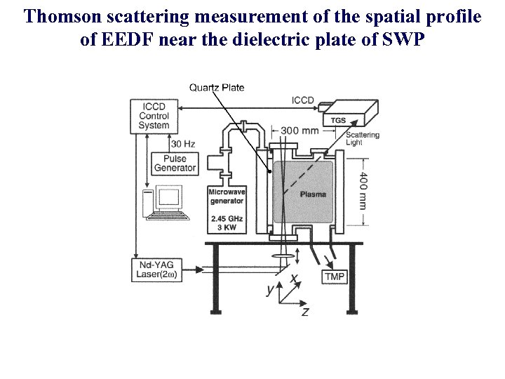
Thomson scattering measurement of the spatial profile of EEDF near the dielectric plate of SWP
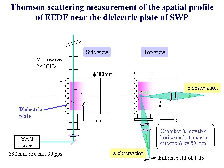
Thomson scattering measurement of the spatial profile of EEDF near the dielectric plate of SWP Side view Top view Microwave 2. 45 GHz f 400 mm z observation Beam x y Dielectric plate YAG laser 532 nm, 330 m. J, 30 pps z z Chamber is movable horizontally ( x and y direction) by 50 mm x observation Entrance slit of TGS
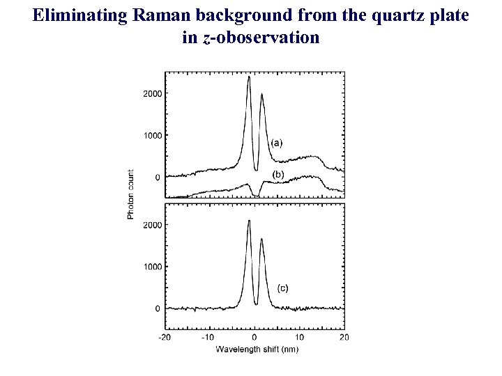
Eliminating Raman background from the quartz plate in z-oboservation
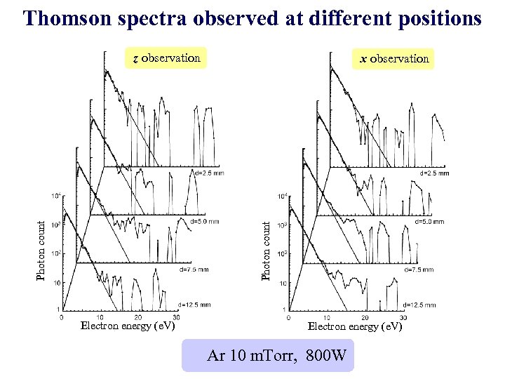
Thomson spectra observed at different positions x observation Photon count z observation Electron energy (e. V) Ar 10 m. Torr, 800 W
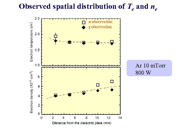
Observed spatial distribution of Te and ne x observation z observation Ar 10 m. Torr 800 W

Microwave E field in SWP Dielectric (quartz) 10 mm E Resonance layer Plasma ne=6. 7× 1011 cm-3 Microwave 2. 45 GHz (wpe=w at nc=7. 4× 1010 cm-3)
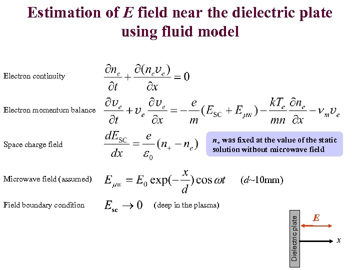
Estimation of E field near the dielectric plate using fluid model Electron continuity Electron momentum balance n+ was fixed at the value of the static solution without microwave field (d~10 mm) Microwave field (assumed) Field boundary condition (deep in the plasma) Dielectric plate Space charge field E x
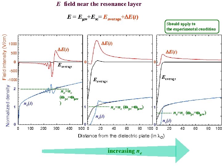
E field near the resonance layer E = Emw+Esc= Eaverage+DE(t) 1000 DE(t) 500 0 DE(t) 0 Eaverage 0 -500 2 ne=nc (wpe=wmw ) ne(t) 1 2 ne=nc (wpe=wmw) 1 1 0 0 Eaverage -1000 Normalized density Field intensity (V/cm) Should apply to the experimental condition 100 200 300 400 0 500 0 1 ne=nc (wpe=wmw) ne(t) 20 40 60 80 0 100 0 ne(t) Distance from the dielectric plate (in l. D) increasing ne 20 40 60 80 100

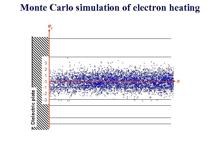
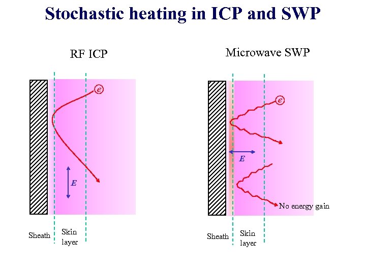
Collisionless electron motion in the resonance E filed (Monte-Carlo simulation) Dielectric plate vx 3 2 1 0 -1 -2 -3 Phase space x 2 e. V Electron bunch 5 e. V ・Low energy electrons are not heated. ・High energy electron are heated by phase randomization caused by ・ sharp spatial change in the microwave field ・ electron reflection by the sheath field
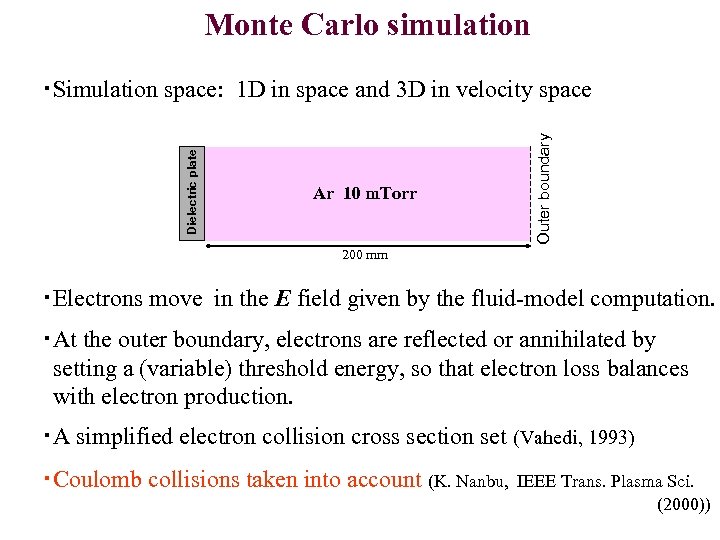
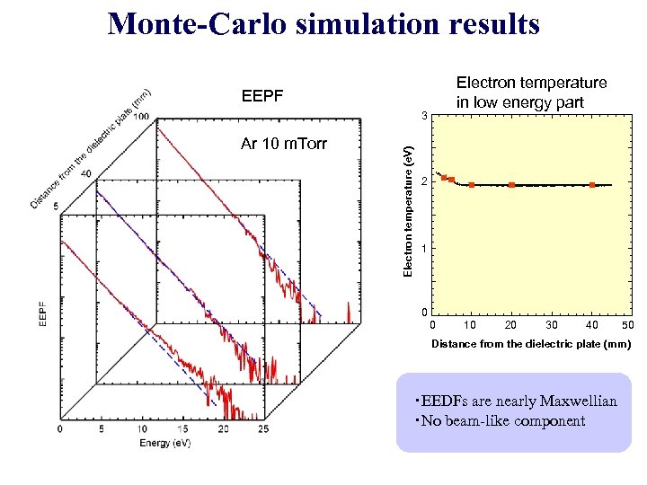
Monte Carlo simulation Ar 10 m. Torr Outer boundary Dielectric plate ・Simulation space: 1 D in space and 3 D in velocity space 200 mm ・Electrons move in the E field given by the fluid-model computation. ・At the outer boundary, electrons are reflected or annihilated by setting a (variable) threshold energy, so that electron loss balances with electron production. ・A simplified electron collision cross section set (Vahedi, 1993) ・Coulomb collisions taken into account (K. Nanbu, IEEE Trans. Plasma Sci. (2000))
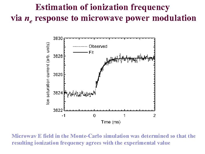
Estimation of ionization frequency via ne response to microwave power modulation Microwav E field in the Monte-Carlo simulation was determined so that the resulting ionization frequency agrees with the experimental value
Monte Carlo simulation of electron heating Dielectric plate vx 3 2 1 0 -1 -2 -3 x
Monte-Carlo simulation results Electron temperature in low energy part EEPF Ar 10 m. Torr Electron temperature (e. V) 3 2 1 0 0 10 20 30 40 50 Distance from the dielectric plate (mm) ・EEDFs are nearly Maxwellian ・No beam-like component
Stochastic heating in ICP and SWP RF ICP Microwave SWP e e E E No energy gain Sheath Skin layer
Summary ・Thomson scattering measurement using TGS + ICCD camera is a powerful method for electron diagnostics of low-temperature plasmas ・In low pressure SWP, the main electron heating mechanism appears to be the stochastic heating via collision of electrons with the resonance layer
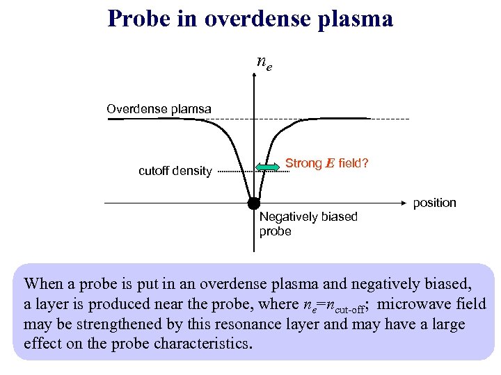
Probe in overdense plasma ne Overdense plamsa cutoff density Strong E field? Negatively biased probe position When a probe is put in an overdense plasma and negatively biased, a layer is produced near the probe, where ne=ncut-off; microwave field may be strengthened by this resonance layer and may have a large effect on the probe characteristics.
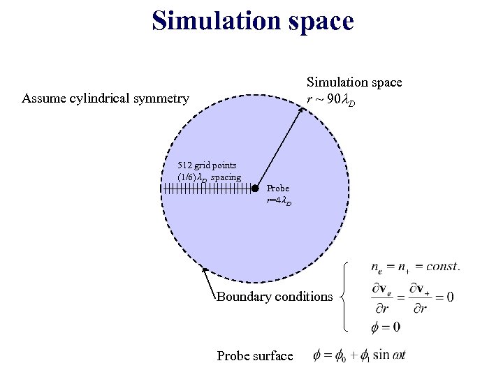
Simulation space r ~ 90 l. D Assume cylindrical symmetry 512 grid points (1/6)l. D spacing Probe r=4 l. D Boundary conditions Probe surface
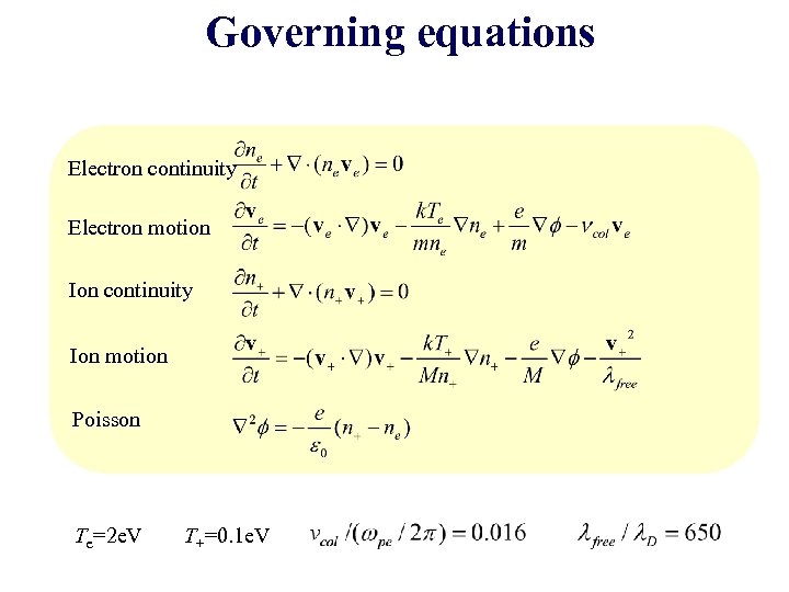
Governing equations Electron continuity Electron motion Ion continuity Ion motion Poisson Te=2 e. V T+=0. 1 e. V
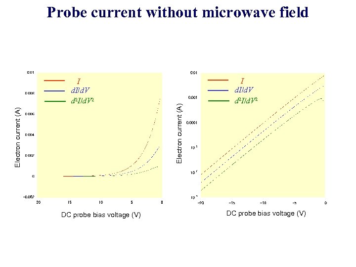
Electron current (A) I d. I/d. V d 2 I/d. V 2 DC probe bias voltage (V) Electron current (A) Probe current without microwave field I d. I/d. V d 2 I/d. V 2 DC probe bias voltage (V)
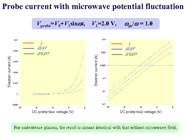
Probe current with microwave potential fluctuation I d. I/d. V d 2 I/d. V 2 DC probe bias voltage (V) V 1=2. 0 V, Electron current (A) Vprobe=V 0+V 1 sinwt, wpe/w = 1. 0 I d. I/d. V d 2 I/d. V 2 DC probe bias voltage (V) For underdense plasma, the result is almost identical with that without microwave field.
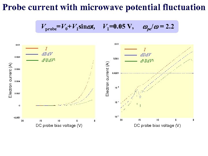
Probe current with microwave potential fluctuation I d. I/d. V d 2 I/d. V 2 DC probe bias voltage (V) V 1=0. 05 V, Electron current (A) Vprobe=V 0+V 1 sinwt, wpe/w = 2. 2 I d. I/d. V d 2 I/d. V 2 DC probe bias voltage (V)
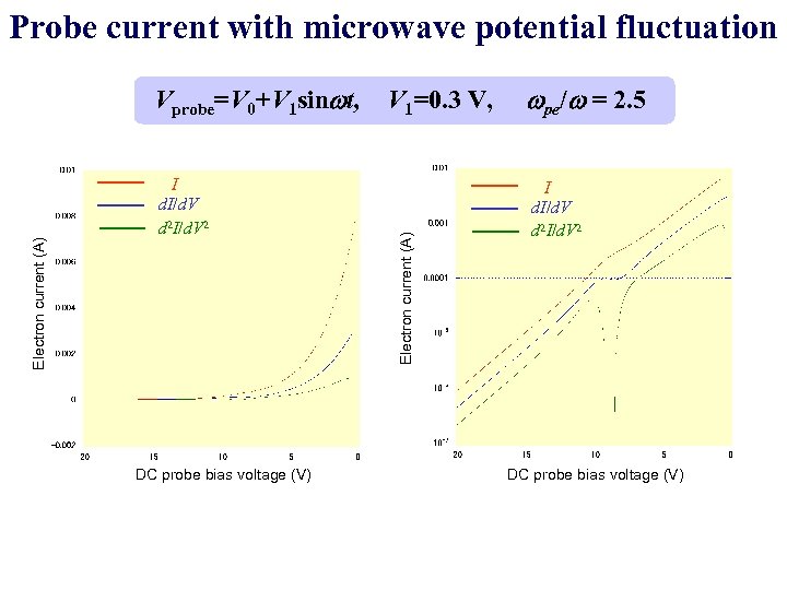
Probe current with microwave potential fluctuation I d. I/d. V d 2 I/d. V 2 DC probe bias voltage (V) V 1=0. 3 V, Electron current (A) Vprobe=V 0+V 1 sinwt, wpe/w = 2. 5 I d. I/d. V d 2 I/d. V 2 DC probe bias voltage (V)

Probe current with microwave potential fluctuation I d. I/d. V d 2 I/d. V 2 DC probe bias voltage (V) V 1=2. 0 V, Electron current (A) Vprobe=V 0+V 1 sinwt, wpe/w = 3. 3 I d. I/d. V d 2 I/d. V 2 DC probe bias voltage (V)
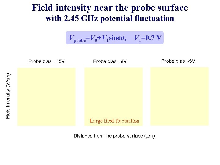
Field intensity near the probe surface with 2. 45 GHz potential fluctuation Vprobe=V 0+V 1 sinwt, Field Intensity (V/cm) Probe bias -15 V V 1=0. 7 V Probe bias -9 V Large filed fluctuation Distance from the probe surface (mm) Probe bias -5 V
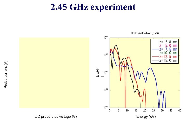
EEPF Probe current (A) 2. 45 GHz experiment DC probe bias voltage (V) Energy (e. V)
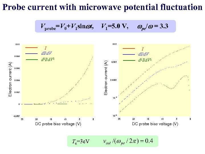
Probe current with microwave potential fluctuation I d. I/d. V d 2 I/d. V 2 V 1=5. 0 V, Electron current (A) Vprobe=V 0+V 1 sinwt, DC probe bias voltage (V) Te=3 e. V wpe/w = 3. 3 I d. I/d. V d 2 I/d. V 2 DC probe bias voltage (V)
Summary When the plasma potential oscillates at a microwave frequency and the plasma is overdense, the probe current is affected in a complicated manner. The distortion in the V-I characteristics may result in false peaks in the second derivative.
ab9df3b112fc9a8e65e4bc4373cd4072.ppt