
Презентация electrical properties


- Размер: 613 Кб
- Количество слайдов: 16
Описание презентации Презентация electrical properties по слайдам
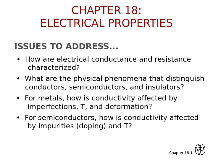
Chapter 18 -ISSUES TO ADDRESS. . . • How are electrical conductance and resistance characterized ? 1 • What are the physical phenomena that distinguish conductors, semiconductors, and insulators? • For metals, how is conductivity affected by imperfections, T, and deformation? • For semiconductors, how is conductivity affected by impurities (doping) and T? CHAPTER 18: ELECTRICAL PROPERTIES
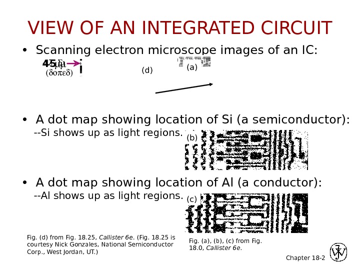
Chapter 18 — 2 • Scanning electron microscope images of an IC: • A dot map showing location of Si (a semiconductor): —Si shows up as light regions. • A dot map showing location of Al (a conductor): —Al shows up as light regions. 0. 5 mm 45 Fig. (a), (b), (c) from Fig. 18. 0, Callister 6 e. Fig. (d) from Fig. 18. 25, Callister 6 e. (Fig. 18. 25 is courtesy Nick Gonzales, National Semiconductor Corp. , West Jordan, UT. ) (a) (b) (c)(d)VIEW OF AN INTEGRATED CIRCUIT
Chapter 18 — 3 • Ohm’s Law: V = I R voltage drop (volts) resistance (Ohms) current (amps) L VI e -A(cross sect. area) • Resistivity, and Conductivity, : —geometry-independent forms of Ohm’s Law Δ V L = I A ρE: electric field intensity resistivity (Ohm-m) J: current density σ= I ρ conductivity • Resistance: R = ρ L A = L A σELECTRICAL CONDUCTION
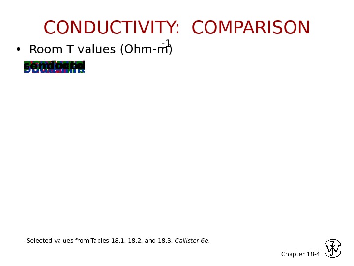
Chapter 18 -insulators Polystyrene <10 -14 Polyethylene 10 -15 -10 -17 Silver 6. 8 x 10 7 Copper 6. 0 x 10 7 Iron 1. 0 x 10 7 METALS Silicon 4 x 10 -4 Germanium 2 x 10 0 Ga. As 10 -6 SEMICONDUCTORS Soda-lime glass 10 -10 Concrete 10 -9 Aluminum oxide <10 -13 CERAMICSPOLYMERSconductorssemiconductors 4 • Room T values (Ohm-m) -1 Selected values from Tables 18. 1, 18. 2, and 18. 3, Callister 6 e. CONDUCTIVITY: COMPARISON
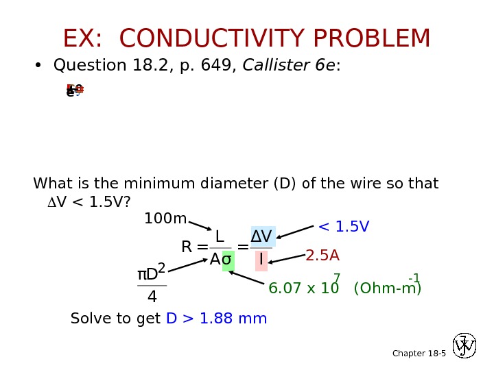
Chapter 18 — 5 • Question 18. 2, p. 649, Callister 6 e : What is the minimum diameter (D) of the wire so that V < 1. 5 V? 100 m. Cu wire. I = 2. 5 A-+ e — R = L A σ = Δ V I 1. 88 mm. EX: CONDUCTIVITY PROBLEM
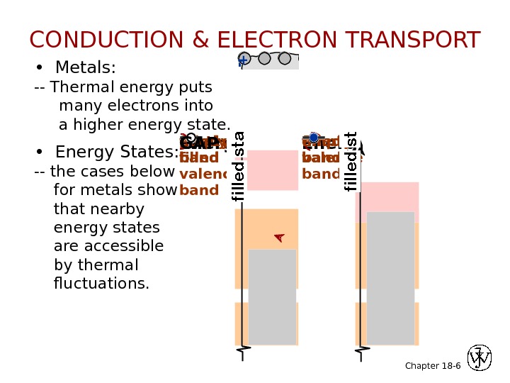
Chapter 18 — 6 • Metals: — Thermal energy puts many electrons into a higher energy state. net e — flow+- • Energy States: — the cases below for metals show that nearby energy states are accessible by thermal fluctuations. Energyfilled bandfilled valence bandempty bandfilled states. CONDUCTION & ELECTRON TRANSPORT filled band. Energypartly filled valence bandempty band. GAPfilled states
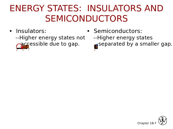
Chapter 18 — 7 • Insulators: —Higher energy states not accessible due to gap. • Semiconductors: —Higher energy states separated by a smaller gap. GAPEnergyfilled bandfilled valence bandempty bandfilled states ? Energyfilled bandfilled valence bandempty bandfilled states. GAPENERGY STATES: INSULATORS AND SEMICONDUCTORS
Chapter 18 — • Imperfections increase resistivity —grain boundaries —dislocations —impurity atoms —vacancies 8 T (°C)-200 -1000 Cu + 3. 32 at%Ni. Cu + 2. 16 at%Nideformed Cu + 1. 12 at%Ni 123456 Resistivity, “ ” These act to scatter electrons so that they take a less direct path. • Resistivity increases with: —temperature —wt% impurity —%CW ρ = ρ thermal + ρ def. Adapted from Fig. 18. 8, Callister 6 e. (Fig. 18. 8 adapted from J. O. Linde, Ann. Physik 5 , p. 219 (1932); and C. A. Wert and R. M. Thomson, Physics of Solids , 2 nd ed. , Mc. Graw-Hill Book Company, New York, 1970. )METALS: RESISTIVITY VS T, IMPURITIES
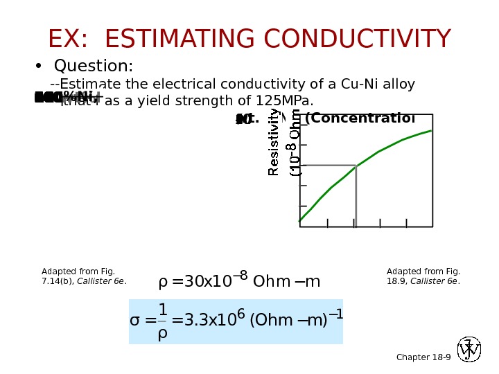
Chapter 18 — 9 • Question: —Estimate the electrical conductivity of a Cu-Ni alloy that has a yield strength of 125 MPa. wt. %Ni, (Concentration C)Resistivity, 21 wt%Ni. Yield strength (MPa)wt. %Ni, (Concentration C) 0102 03 04 05 0608 010 0120140160180 ρ=30 x 10 − 8 Ohm−m σ = 1 ρ = 3. 3 x 10 6 ( Ohm − m ) − 1 Adapted from Fig. 18. 9, Callister 6 e. Adapted from Fig. 7. 14(b), Callister 6 e. EX: ESTIMATING CONDUCTIVITY
Chapter 18 — 10 • Data for Pure Silicon : — increases with T —opposite to metals σ undoped ∝ e − E gap / k. T ? Energyfilled bandfilled valence bandempty bandfilled states. GAP electrons can cross gap at higher T material Si Ge Ga. P Cd. S band gap (e. V) 1. 11 0. 67 2. 25 2. 40 Adapted from Fig. 19. 15, Callister 5 e. (Fig. 19. 15 adapted from G. L. Pearson and J. Bardeen, Phys. Rev. 75 , p. 865, 1949. ) Selected values from Table 18. 2, Callister 6 e. PURE SEMICONDUCTORS: CONDUCTIVITY VS T electrical conductivity,
Chapter 18 — • Electrical Conductivity given by: σ=neμe+peμh 11# electrons/m 3 electron mobility # holes/m 3 hole mobility • Concept of electrons and holes: +-electron hole pair creation+- no applied electric fieldvalence electron. Si atom applied electric fieldelectron hole pair migration Adapted from Fig. 18. 10, Callister 6 e. CONDUCTION IN TERMS OF ELECTRON AND HOLE MIGRATION
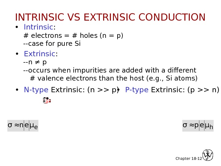
Chapter 18 — 12 • Intrinsic : # electrons = # holes (n = p) —case for pure Si • Extrinsic : —n ≠ p —occurs when impurities are added with a different # valence electrons than the host (e. g. , Si atoms) • N-type Extrinsic: (n >> p) • P-type Extrinsic: (p >> n) σ≈neμe σ≈peμh 4 +4 +4 +4 + no applied electric field 5+4 +4 +4 +Phosphorus atom no applied electric field. Boron atomvalence electron. Si atomconduction electronhole 3 +INTRINSIC VS EXTRINSIC CONDUCTION
Chapter 18 -doped 0. 0013 at%B 0. 0052 at%B electrical conductivity, 13 • Data for Doped Silicon : — increases doping —reason: imperfection sites lower the activation energy to produce mobile electrons. Adapted from Fig. 19. 15, Callister 5 e. (Fig. 19. 15 adapted from G. L. Pearson and J. Bardeen, Phys. Rev. 75 , p. 865, 1949. ) • Comparison: intrinsic vs extrinsic conduction. . . —extrinsic doping level: 10 21 /m 3 of a n-type donor impurity (such as P). —for T < 100 K: "freeze-out" thermal energy insufficient to excite electrons. —for 150 K < T > 450 K: «intrinsic»undopedconduction electron concentration (10 21 /m 3 )T (K) 6004 002 0000123 freeze-outextrinsicin trinsicdoped Adapted from Fig. 18. 16, Callister 6 e. (Fig. 18. 16 from S. M. Sze, Semiconductor Devices, Physics, and Technology , Bell Telephone Laboratories, Inc. , 1985. )DOPED SEMICON: CONDUCTIVITY VS T
Chapter 18 — 14 • Allows flow of electrons in one direction only (e. g. , useful to convert alternating current to direct current. • Processing: diffuse P into one side of a B-doped crystal. • Results: —No applied potential: no net current flow. —Forward bias: carrier flow through p-type and n-type regions; holes and electrons recombine at p-n junction; current flows. —Reverse bias: carrier flow away from p-n junction; carrier conc. greatly reduced at junction; little current flow. p -typen -type +++++——p -typen -type +- +++++——p -typen -type -+P-N RECTIFYING JUNCTION
Chapter 18 — 15 • Electrical conductivity and resistivity are: —material parameters. —geometry independent. • Electrical resistance is: —a geometry and material dependent parameter. • Conductors, semiconductors, and insulators. . . —different in whethere accessible energy states for conductance electrons. • For metals, conductivity is increased by —reducing deformation —reducing imperfections —decreasing temperature. • For pure semiconductors, conductivity is increased by —increasing temperature —doping (e. g. , adding B to Si (p-type) or P to Si (n-type). SUMMARY
Chapter 18 -Reading: Core Problems: Self-help Problems: 0 ANNOUNCEMENTS