6ef9ce368f6f552720cfb8ed52208467.ppt
- Количество слайдов: 32
 EE 437 Spring 2006 Advanced Computer Architecture Lecture 14 Project 4 review Write-back cache correction Write buffer Performance Lillevik 437 s 06 -l 14 University of Portland School of Engineering 1
 EE 437 Spring 2006 Project 4 team review • Team Dog Lillevik 437 s 06 -l 14 University of Portland School of Engineering 2
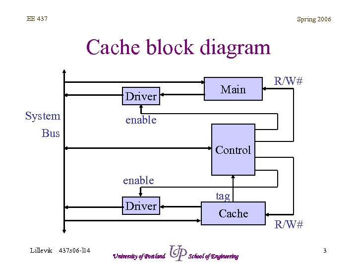 EE 437 Spring 2006 Cache block diagram Driver System Bus Main R/W# enable Control enable Driver Lillevik 437 s 06 -l 14 University of Portland tag Cache School of Engineering R/W# 3
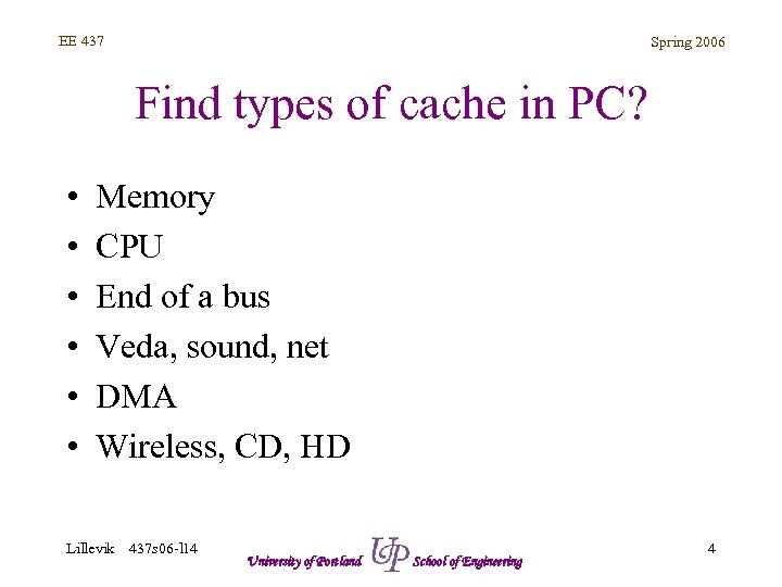 EE 437 Spring 2006 Find types of cache in PC? • • • Memory CPU End of a bus Veda, sound, net DMA Wireless, CD, HD Lillevik 437 s 06 -l 14 University of Portland School of Engineering 4
 EE 437 Spring 2006 Write-back, cache hit • Read – Data provided by cache memory – Fast • Write – Data written to cache (fast) – Data NOT written to memory, inconsistency exists Lillevik 437 s 06 -l 14 University of Portland School of Engineering 5
 EE 437 Spring 2006 Write-back, cache miss • Two cases – Memory and cache consistent – Memory and cache inconsistent (cache has correct data) • Called modified • Called dirty • All misses to inconsistent cache and memory require a write-back cycle first Lillevik 437 s 06 -l 14 University of Portland School of Engineering 6
 EE 437 Spring 2006 Write-back, read miss • Cache consistent – Data provided by main memory (slow) – Data also written to cache (update) • Cache inconsistent – Data in cache written to memory (slow): WB – Data provided by main memory (slow) – Data also written to cache (update) Lillevik 437 s 06 -l 14 University of Portland School of Engineering 7
 EE 437 Spring 2006 Write-back, write miss • Cache consistent – Data written to cache (fast) – Data NOT written to memory, inconsistency exists • Cache inconsistent – Data in cache written to memory (slow): WB – Data written to cache (fast) – Data NOT written to memory, inconsistency exists Lillevik 437 s 06 -l 14 University of Portland School of Engineering 8
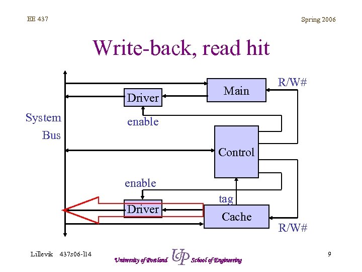 EE 437 Spring 2006 Write-back, read hit Driver System Bus Main R/W# enable Control enable Driver Lillevik 437 s 06 -l 14 University of Portland tag Cache School of Engineering R/W# 9
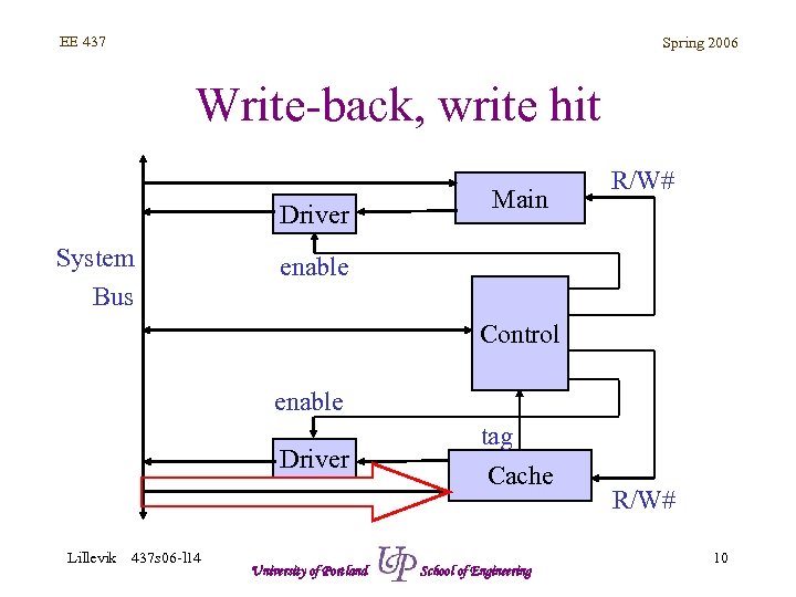 EE 437 Spring 2006 Write-back, write hit Driver System Bus Main R/W# enable Control enable Driver Lillevik 437 s 06 -l 14 University of Portland tag Cache School of Engineering R/W# 10
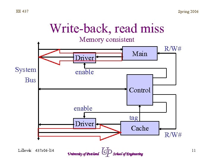 EE 437 Spring 2006 Write-back, read miss Memory consistent Driver System Bus Main R/W# enable Control enable Driver Lillevik 437 s 06 -l 14 University of Portland tag Cache School of Engineering R/W# 11
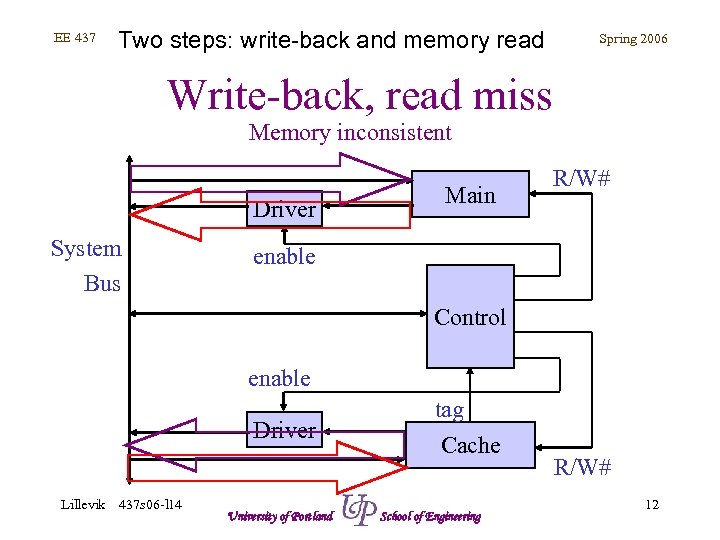 EE 437 Two steps: write-back and memory read Spring 2006 Write-back, read miss Memory inconsistent Driver System Bus Main R/W# enable Control enable Driver Lillevik 437 s 06 -l 14 University of Portland tag Cache School of Engineering R/W# 12
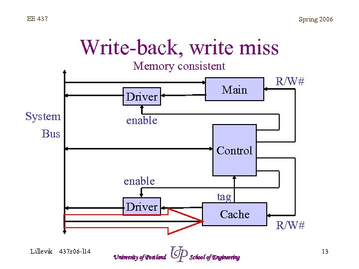 EE 437 Spring 2006 Write-back, write miss Memory consistent Driver System Bus Main R/W# enable Control enable Driver Lillevik 437 s 06 -l 14 University of Portland tag Cache School of Engineering R/W# 13
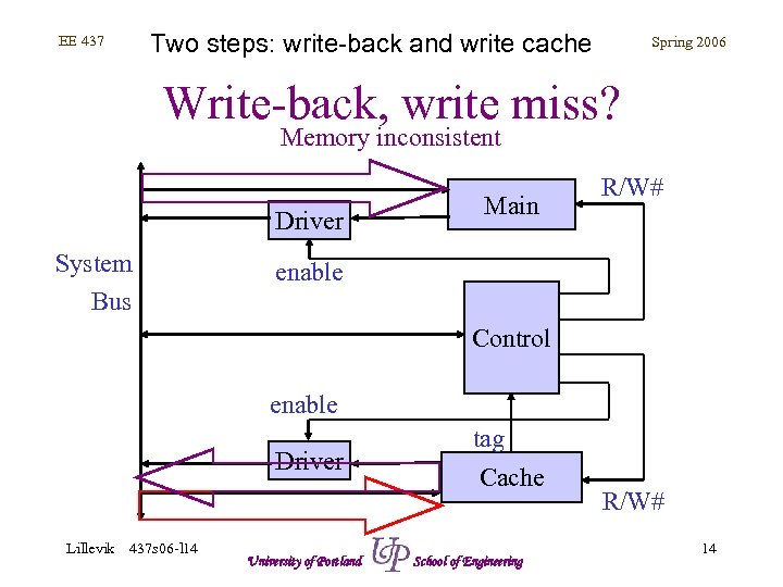 Two steps: write-back and write cache EE 437 Spring 2006 Write-back, write miss? Memory inconsistent Driver System Bus Main R/W# enable Control enable Driver Lillevik 437 s 06 -l 14 University of Portland tag Cache School of Engineering R/W# 14
 EE 437 Spring 2006 Cache example • • • CPU: our B 2 Logic model Memory of 32 words Cache of 8 words Direct mapped Cache and memory at an initial state Lillevik 437 s 06 -l 14 University of Portland School of Engineering 15
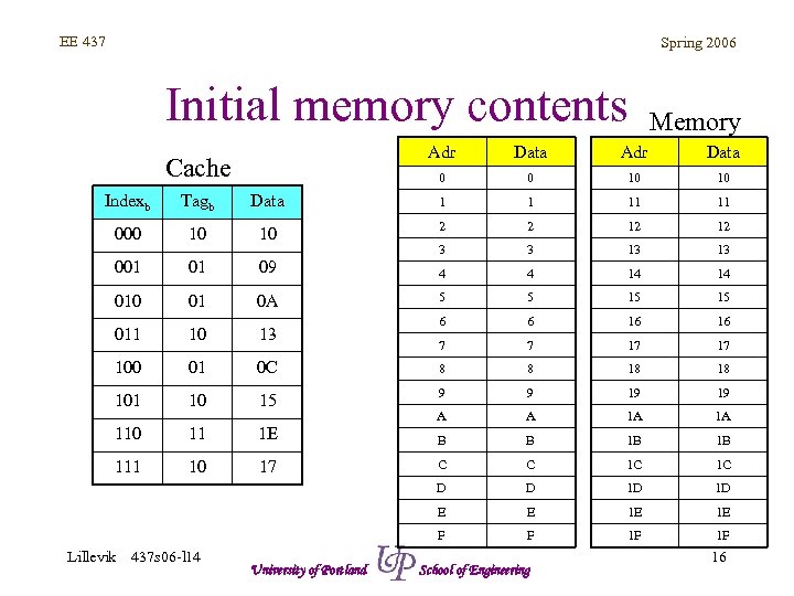 EE 437 Spring 2006 Initial memory contents Memory Adr Data 0 Cache Data 0 10 10 Indexb Tagb Data 1 1 11 11 000 10 10 2 2 12 12 3 3 13 13 001 01 09 4 4 14 14 010 01 0 A 5 5 15 15 011 10 13 6 6 16 16 7 7 17 17 100 01 0 C 8 8 18 18 101 10 15 9 9 19 19 110 11 1 E A A 1 A 1 A B B 1 B 1 B 111 10 17 C C 1 C 1 C D D 1 D 1 D E E 1 E 1 E F F 1 F 1 F Lillevik 437 s 06 -l 14 University of Portland School of Engineering 16
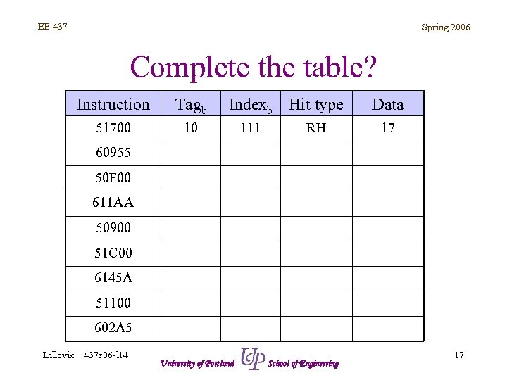 EE 437 Spring 2006 Complete the table? Instruction Tagb 51700 Indexb Hit type 10 111 RH Data 17 60955 50 F 00 611 AA 50900 51 C 00 6145 A 51100 602 A 5 Lillevik 437 s 06 -l 14 University of Portland School of Engineering 17
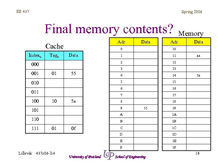 EE 437 Spring 2006 Final memory contents? Adr Cache Indexb 10 5 a 13 4 14 15 16 7 011 12 6 55 11 5 01 1 3 Data 17 8 18 9 101 55 B Lillevik 437 s 06 -l 14 University of Portland C 1 C 1 D 1 E F 0 f 1 B E 01 5 a 1 A D 111 aa 19 A 110 Data 10 2 Tagb 010 100 Adr 0 001 Data Memory 1 F School of Engineering 18
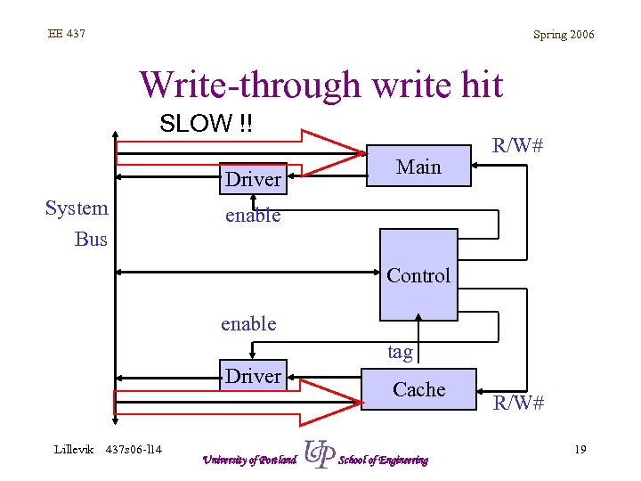 EE 437 Spring 2006 Write-through write hit SLOW !! Driver System Bus Main R/W# enable Control enable tag Driver Lillevik 437 s 06 -l 14 University of Portland Cache School of Engineering R/W# 19
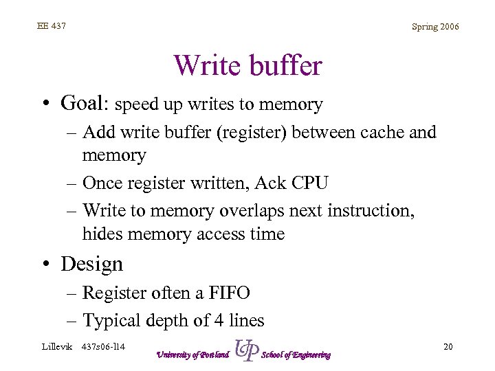 EE 437 Spring 2006 Write buffer • Goal: speed up writes to memory – Add write buffer (register) between cache and memory – Once register written, Ack CPU – Write to memory overlaps next instruction, hides memory access time • Design – Register often a FIFO – Typical depth of 4 lines Lillevik 437 s 06 -l 14 University of Portland School of Engineering 20
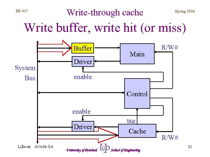 Write-through cache EE 437 Spring 2006 Write buffer, write hit (or miss) Buffer System Bus Driver Main R/W# enable Control enable Driver Lillevik 437 s 06 -l 14 University of Portland tag Cache School of Engineering R/W# 21
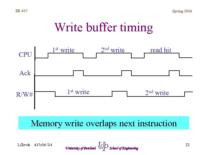 EE 437 Spring 2006 Write buffer timing CPU 1 st write 2 nd write read hit Ack 1 st write R/W# 2 nd write Memory write overlaps next instruction Lillevik 437 s 06 -l 14 University of Portland School of Engineering 22
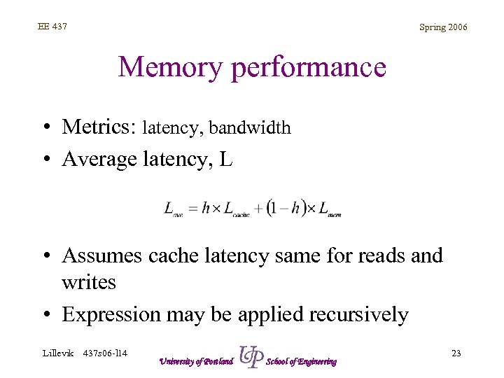 EE 437 Spring 2006 Memory performance • Metrics: latency, bandwidth • Average latency, L • Assumes cache latency same for reads and writes • Expression may be applied recursively Lillevik 437 s 06 -l 14 University of Portland School of Engineering 23
 EE 437 Spring 2006 Find average latency? • • CPU clocked at 1. 5 GHz DDR memory speed is 500 MHz Cache cycle time is 100 ps Hit rate is 0. 95 Lillevik 437 s 06 -l 14 University of Portland School of Engineering 24
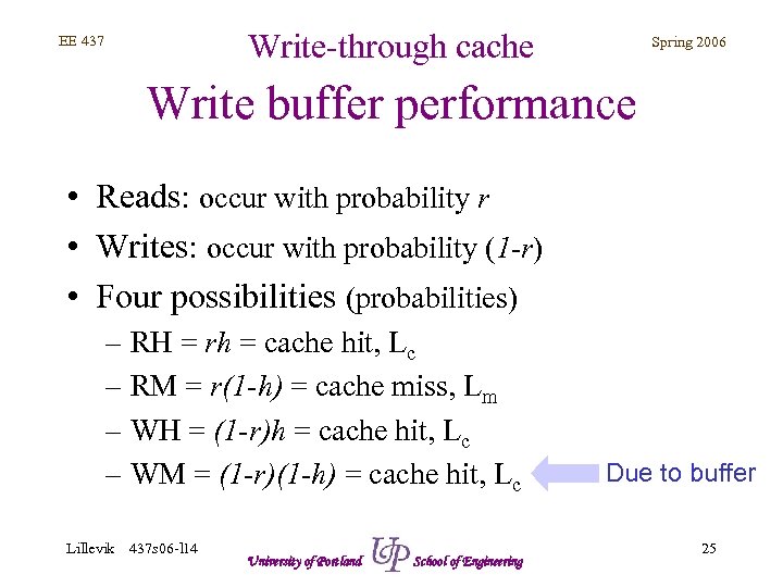 Write-through cache EE 437 Spring 2006 Write buffer performance • Reads: occur with probability r • Writes: occur with probability (1 -r) • Four possibilities (probabilities) – RH = rh = cache hit, Lc – RM = r(1 -h) = cache miss, Lm – WH = (1 -r)h = cache hit, Lc – WM = (1 -r)(1 -h) = cache hit, Lc Lillevik 437 s 06 -l 14 University of Portland School of Engineering Due to buffer 25
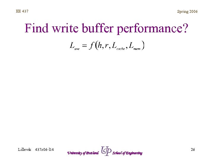 EE 437 Spring 2006 Find write buffer performance? Lillevik 437 s 06 -l 14 University of Portland School of Engineering 26
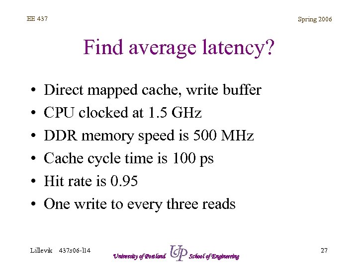 EE 437 Spring 2006 Find average latency? • • • Direct mapped cache, write buffer CPU clocked at 1. 5 GHz DDR memory speed is 500 MHz Cache cycle time is 100 ps Hit rate is 0. 95 One write to every three reads Lillevik 437 s 06 -l 14 University of Portland School of Engineering 27
 EE 437 Lillevik Spring 2006 437 s 06 -l 14 University of Portland School of Engineering 28
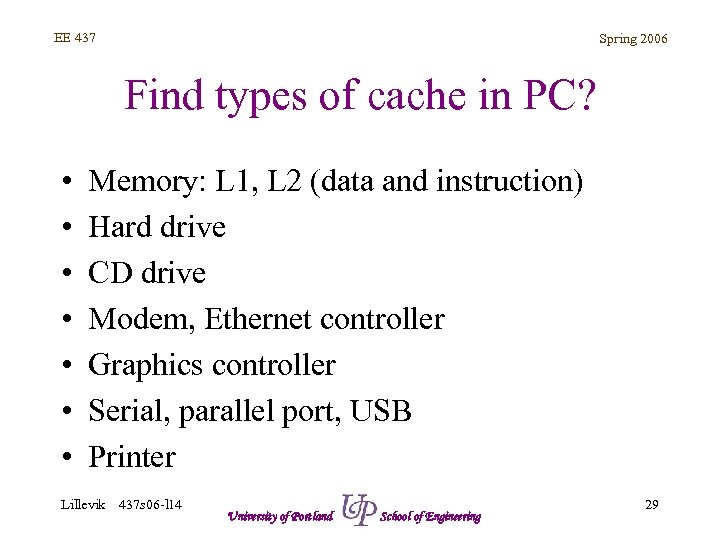 EE 437 Spring 2006 Find types of cache in PC? • • Memory: L 1, L 2 (data and instruction) Hard drive CD drive Modem, Ethernet controller Graphics controller Serial, parallel port, USB Printer Lillevik 437 s 06 -l 14 University of Portland School of Engineering 29
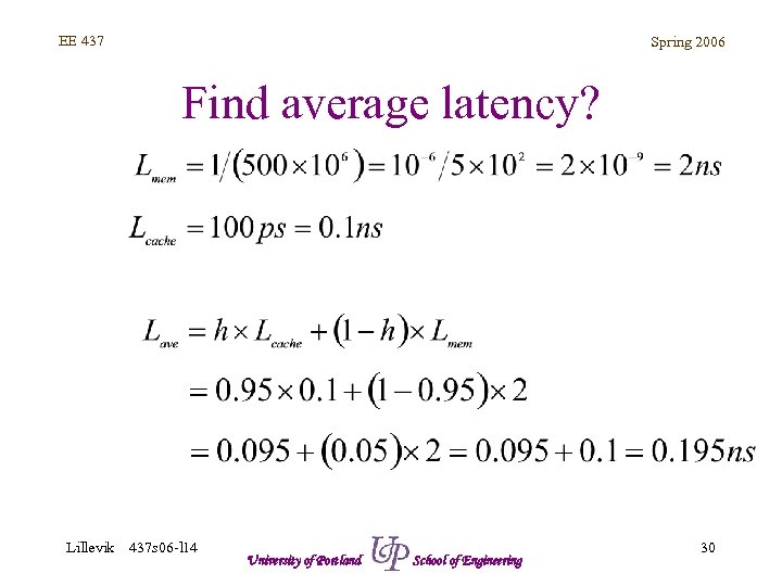 EE 437 Spring 2006 Find average latency? Lillevik 437 s 06 -l 14 University of Portland School of Engineering 30
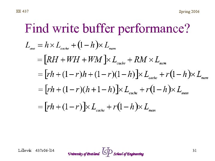 EE 437 Spring 2006 Find write buffer performance? Lillevik 437 s 06 -l 14 University of Portland School of Engineering 31
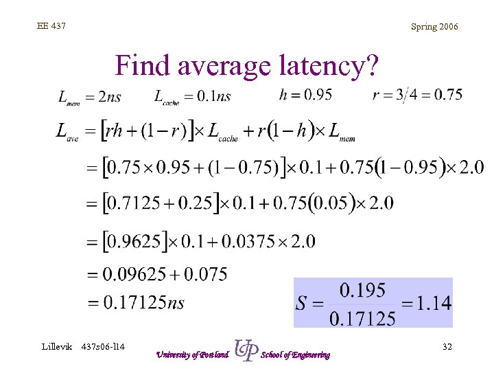 EE 437 Spring 2006 Find average latency? Lillevik 437 s 06 -l 14 University of Portland School of Engineering 32


