
30. 01. 16 1 Lecture 4 Plasma Etching


processes_for_micromachining-lecture_4.ppt
- Размер: 1.1 Mегабайта
- Количество слайдов: 43
Описание презентации 30. 01. 16 1 Lecture 4 Plasma Etching по слайдам
30. 01. 16 1 Lecture 4 Plasma Etching • Plasma (or dry) etching is a key process in the semiconductor industry. Companies such as Applied Materials, Inc. , of Santa Clara, California, and Lam. Research Corp. of Fremont, California, are leading developers and suppliers of plasma-etching systems of silicon as well as silicon dioxide, silicon nitride, and a wide variety of metals. • Conventional plasma-phase etch processes are commonly used for etching polysilicon in surface micromachining and for the formation of shallow cavities in bulk micromachining. The introduction in the mid 1990 s of deep reactive ion etching (DRIE) systems by Surface Technology Systems (STS), Ltd. , of Newport, United Kingdom, Unaxis Semiconductors (formerly Plasma. Therm) of St. Petersburg, Florida, and Alcatel, S. A. , of Paris, France, provided a new powerful tool for the etching of very deep trenches (over 500 µm) with nearly vertical sidewalls.
30. 01. 16 2 • Plasma etching involves the generation of chemically reactive neutrals (e. g. , F, Cl), and ions (e. g. , SF x + ) that are accelerated under the effect of an electric field toward a target substrate. • The reactive species (neutrals and ions) are formed by the collision of molecules in a reactant gas (e. g. , SF 6 , CF 4 , Cl 2 , CCl. F 3 , NF 3 ) with a cloud of energetic electrons excited by an RF electric field. • When the etch process is purely chemical, powered by the spontaneous reaction of neutrals with silicon, it is plasma etching. • I f ion bombardment of the silicon surface plays a synergistic role in the chemical etch reaction, the process is reactive ion etching (RIE). In RIE, ion (e. g. , SF x + ) motion toward the substrate is nearly vertical, which gives RIE vertical anisotropy.
30. 01. 16 3 • Asymmetric electrodes and low chamber pressures (5 Pa) are characteristic of RIE operation. • Inductively coupled plasma reactive ion etching (ICP-RIE) provides greater excitation to the electron cloud by means of an externally applied RF electromagnetic field. • Inductively coupled plasma (ICP) increases the density of ions and neutrals resulting in higher etch rates. The ion bombardment energy is controlled by a separate power supply driving the platen ( держатель) on which the wafer sits.
30. 01. 16 4 • A different, purely physical method of etching is ion milling, in which noble-gas ions (usually argon) are remotely generated, then accelerated at the substrate though a potential on the order of 1 k. V. • The directionality of the ions results in a very vertical etch profile. Because a chemical reaction is not required, any material can be etched by ion milling. • The ion-milling rate is typically much slower than with RIE and varies widely with the material.
30. 01. 16 5 Deep Reactive ion Etching ( DRIE ) • DRIE evolved in the mid 1990 s from the need within the micromachining community for an etch process capable of vertically etching high-aspect-ratio trenches at rates substantially larger than the 0. 1 to 0. 5 µm/min typical of traditional plasma and RIE etchers. • In one approach, developed by Alcatel, the wafer is cooled to cryogenic temperatures. Condensation of the reactant gases (SF 6 and O 2 ) protects the sidewalls from etching by the reactive fluorine atoms. • However, cryogenic cooling may be difficult to maintain locally and could result in undesirable thermal stresses.
30. 01. 16 6 • Another approach currently used by Alcatel, Plasma. Therm, and Surface Technology Systems (STS) follows a method patented by Robert Bosch Gmb. H, of Stuttgart, Germany, in which etch and deposition steps alternate in an ICP-RIE system (see Table 3. 3). • The etch part of the cycle, typically lasting 5 to 15 s, uses SF 6 , which supplies highly reactive fluorine radicals, to etch silicon.
30. 01. 16 7 • The etch step has both vertical and isotropic character, resulting in a slight mask undercut (see Figure 3. 12). • In the deposition step, a fluorocarbon polymer (made of a chain of CF 2 groups similar in composition to Teflon™), about 10 nm thick, is plasma-deposited using C 4 F 8 as the source gas. In the following etch step, the vertically oriented ions (SF x+ ) enhance the effect of fluorine radicals in removing the protective polymer at the bottom of the trench, while the film remains relatively intact ( неповрежденный) along the sidewalls.
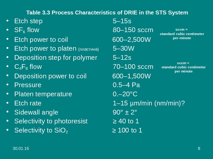
30. 01. 16 8 Table 3. 3 Process Characteristics of DRIE in the STS System • Etch step 5– 15 s • SF 6 flow 80– 150 sccm • Etch power to coil 600– 2, 500 W • Etch power to platen (пластина) 5– 30 W • Deposition step for polymer 5– 12 s • C 4 F 8 flow 70– 100 sccm • Deposition power to coil 600– 1, 500 W • Pressure 0. 5– 4 Pa • Platen temperature 0. – 20°C • Etch rate 1– 15 µm/min (nm/min)? • Sidewall angle 90° ± 2° • Selectivity to photoresist ≥ 40 to 1 • Selectivity to Si. O 2 ≥ 100 to 1 sccm = standard cubic centimeter per minute
30. 01. 16 9 scalloping effect = эффект гребешка is exagerrate d = усилен
30. 01.
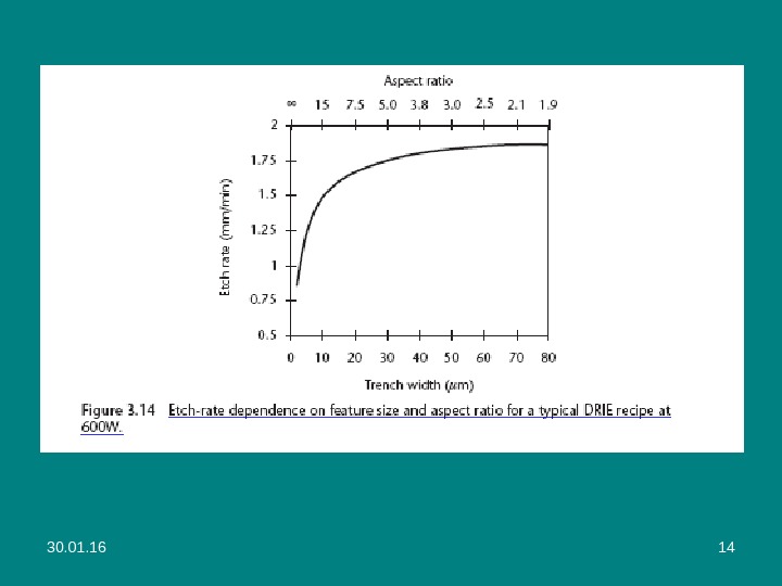
30. 01. 16 11 • The repetitive alternation of the etch and passivation steps results in a very directional etch at rates from 1 to over 15 µm/min, depending on the recipe and machine (newer etchers are available with more powerful RF sources). • The degree of scalloping—the sidewall texture due to the isotropic component of the etch—varies with the recipe. • Recipes optimized for smoother sidewalls can exhibit surface planarity with roughness less than 50 nm, allowing their use as optically reflective surfaces. • A limitation of DRIE is the dependence of the etch rates on the aspect ratio (ratio of height to width) of the trench (see Figures 3. 13 and 3. 14). The effect is known as lag (отставание) or aspect-ratio-dependent etching (ARDE).
30. 01. 16 12 • The etch rate is limited by the flux of reactants (namely, F radicals) and drops significantly for narrow trenches. • A quick remedy (средство) is implemented (внедренное) at the mask layout stage by eliminating (устран ением ) l arge disparities (диспропорции) in trench widths. The effect of lag can also be greatly alleviated by adjusting the process parameters such that a balance is reached between the transport-limited rates of the etch and passivation steps. • These parameters are found with experimentation and may vary depending on the mask layout. The penalty for minimizing lag is a reduction in the etch rate to about 1 µm/min.
30. 01. 16 13 Figure 3. 13 ARDE in DRIE. The etch rate decreases with increasing trench aspect ratio. ( Courtesy of: GE Nova. Sensor of Fremont, California. )
30. 01.
30. 01. 16 15 • The high selectivity to silicon dioxide makes it possible to etch deep trenches and stop on a buried layer of silicon dioxide (e. g. , silicon-on-insulator wafers). • W hen the etch reaches the buried oxide layer, the positive ions charge the oxide, deflecting subsequent (отклоняют последующие ионы) ions to the side. • The ion bombardment degrades ( понижать ) the passivation layer at the bases of the sidewalls, resulting in an undesirable lateral undercut (referred to as footing or notching ( выемка ) ) along the silicon-oxide interface (see Figure 3. 15). The problem is eliminated ( устранять ) in STS DRIE tools by reducing the platen frequency from 13. 56 MHz to 380 k. Hz, which alters (изменять) the ion energy.
30. 01.
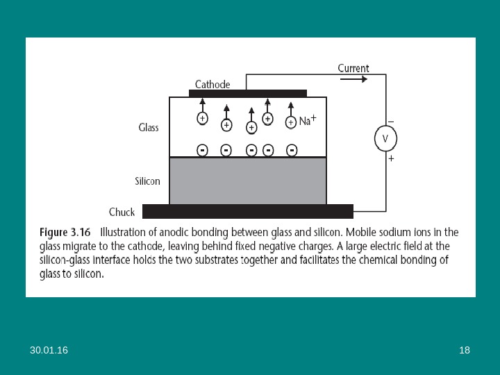
30. 01. 16 17 Advanced Process Tools Anodic Bonding • Anodic bonding, also known as field-assisted bonding or Mallory bonding, is a simple process to join together a silicon wafer and a sodium-containing glass substrate (e. g. , Corning Pyrex® 7740 and 7070, Schott 8330 and 8329). • It is used in the manufacturing of a variety of sensors, including pressure sensors, because it provides a rigid support to the silicon that mechanically isolates it from packaging stress. • The bonding is performed at a temperature between 200° and 500°C in vacuum, air, or in an inert gas environment. • The application of 500 to 1, 500 V across the two substrates, with the glass held at the negative potential, causes mobile positive ions (mostly Na+) in the glass to migrate away from the silicon-glass interface toward the cathode, leaving behind fixed negative charges in the glass (see Figure 3. 16)
30. 01.
30. 01. 16 19 • The bonding is complete when the ion current (measured externally as an electron current) vanishes, indicating that all mobile ions have reached the cathode. • The electrostatic attraction between the fixed negative charge in the glass and positive mirror charge induced in the silicon holds the two substrates together and facilitates ( способствует ) the chemical bonding of glass to silicon. • Silicon dioxide on the silicon surface should be removed before bonding, as a thin (~100 nm) layer is sufficient to disturb (нарушить) the current flow and the bond. • A buried oxide layer, such as on a silicon-on-insulator (SOI) wafer, however, does not present a problem, as it conducts sufficiently well at high temperatures to allow the current flow needed for bonding.
30. 01. 16 20 • The coefficient of thermal expansion of the glass substrate is preferably matched to that of silicon in order to minimize thermal stresses. • For example, Corning Pyrex® 7740 has a coefficient of thermal expansion of 3. 2 10− 6 /°C; silicon’s coefficient is 2. 6 · 10 − 6 /°C at room temperature, rising to 3. 8 · 10− 6 /°C at 300°C. • Sputtered, evaporated, or spin-on glass films containing sodium can also be used to anodically bond two silicon substrates. • In this case, the required voltage to initiate the bond process decreases to less than 100 V due to the thinness of the glass layer.
30. 01. 16 21 Silicon Direct Bonding • Silicon direct bonding, also known as silicon fusion bonding, is a process capable of securely joining two silicon substrates. It emerged as an important step in the development of SOI technology during the 1980 s for high-frequency and radiation-hard CMOS applications. • SOI wafers made by silicon direct bonding are commercially available today from many vendors. • The concept was quickly extended to the manufacture of pressure sensors and accelerometers in the late 1980 s and is now an important technique in the MEMS toolbox.
30. 01. 16 22 • Silicon direct bonding can be performed between two bare single-crystal silicon surfaces or polished polysilicon. • One or both surfaces may have thermal or other smooth silicon dioxide or silicon nitride on them. • For uniform and void-free bonding, the surfaces must be free of particles and chemica l contamination, flat to within about 5 µm across a 100 -mm wafer, and smoother than about 0. 5 — to 1 -nm RMS roughness (silicon wafers out of the box are typically on the order of 0. 1– 0. 2 nm RMS roughness).
30. 01. 16 23 • The direct bonding process starts with cleaning and hydration of the surfaces. • The following is a typical sequence, although one or more steps may be swapped (менять местами) or even skipped (пропускать) , as long as (поскольку) the resulting wafers are clean and hydrated. • First, the wafers are precleaned in a hot Piranha (sulfuric acid and hydrogen peroxide) solution. • Next, they are dipped in a dilute HF solution to etch away the native oxide (or thermal oxide surface) and remove contaminants trapped in the oxide. • This is followed by an RCA-1 clean (hot ammonium hydroxide and hydrogen peroxide solution) clean, intended to remove organics. Werner Kern developed the basic procedure in 1965 while working for RCA, the Radio Corporation of America.
30. 01. 16 24 • Finally, an RCA-2 clean (hot hydrochloric acid and hydrogen peroxide solution) is done to remove metal contamination. • All of the hot hydrogen-peroxide solutions form the hydroxyl (–OH) groups on the surface needed for bonding. This is known as hydration. • The bond surfaces are then carefully brought into contact and held together by van der Waals forces. • An anneal at 800° to 1, 100°C for a few hours promotes and strengthens the bond according to the reaction:
30. 01. 16 25 • In some cases, features on the two bond surfaces must be aligned to each other prior to bonding. For instance, a cavity in one wafer may be joined to an access port provided through the second wafer. • Special equipment is necessary to perform the alignment and bonding. SUSS Micro. Tec and EV Group, two major equipment manufacturers, use similar schemes to align and bond. • The wafers are sequentially mounted in a special fixture and aligned with the two bond surfaces facing each other in a manner similar to double-sided alignment in lithography.
30. 01. 16 26 • A mechanical clamping fixture holds the aligned wafers in position, separated by thin spacers at the wafer edges. • If desired, the fixture and wafers can be placed in a chamber with vacuum, inert gas, oxygen, or other controlled atmosphere. • The centers of the wafers are then brought into contact and the spacers removed, allowing the bonded area to proceed from the wafer center to the edge. • The relative misalignment is routinely less than 5 µm and can be as good as 1 µm. • Direct bonding can be repeated to form thick multiple-wafer stacks, although experience shows that the thicker the stack becomes, the more difficult it is to achieve good bonding.
30. 01. 16 27 Grinding ( шлифовка) , Polishing, and Chemical-Mechanical Polishing • Some applications use a thin layer of silicon (5 to 200 µm) that is fusion-bonded to a standard-thickness wafer (525 µm for single-side polished or 400 µm for doubleside-polished, 100 -mm-diameter wafers), possibly with a layer of oxide between them. • Instead of attempting to silicon-fusion bond such a thin, fragile layer to a standard-thickness wafer, two standard-thickness wafers are fusion bonded together, then one side is thinned down to the desired thickness.
30. 01. 16 28 • The thickness reduction is achieved using grinding and polishing. The wafer stack is mounted on a rotating table and ground by a diamond-bonded wheel spinning in the opposite direction. • The grinding mechanically abrades (сдирать) silicon and reduces the thickness of the wafer to near the desired thickness. Hundreds of micrometers can be removed. • The resulting surface roughness is removed in the subsequent polishing step in which wafers are mounted inside precise templates on a rotating table.
30. 01. 16 29 • A wheel with a felt-like (фетровый) texture polishes the wafer surface using a slurry containing fine silica or other hard particles in a very dilute alkaline solution (see Figure 3. 17). • The final surface is smooth, with a thickness control as good as ± 0. 5 µm. • There is frequently invisible damage to the crystal structure incurred during the grinding step that becomes apparent when etched in orientation-dependent etchants. • This damage can be removed by growing a thick thermal oxide, then etching it off.
30. 01. 16 30 • Chemical mechanical polishing, also known as chemical mechanical planarization (CMP), is commonly used in the IC industry for the planarization of dielectric insulating layers. • The polishing combines mechanical action with chemical etching using an abrasive slurry dispersed in an alkaline solution (p. H > 10). • The rate of material removal is controlled by the slurry flow and p. H, applied pressure on the polishing head, rotational speed, and operating temperature. • CMP is an excellent planarization method yielding a surface roughness less than 1 nm over large dimensions, but it is slow with removal rates less than 100 nm/min compared to 1 µm/min for standard polishing.
30. 01. 16 31 Водор дный показ тельоо ао • Водор дный показ тель оо ао , p. H (произносится «пэ аш» , английское произношение англ. p. H — pi: e t ɪ ʃ , «пи эйч» ) — мера активности (в очень разбавленных растворах она эквивалентна концентрации ) ионов водорода в растворе , и количественно выражающая его кислотность, вычисляется как отрицательный (взятый с обратным знаком) десятичный логарифм активности водородных ионов, выраженной в молях на один литр:
30. 01. 16 32 Вывод значения p. H • В чистой воде при 25 °C концентрации ионов водорода ([H+ ]) и гидроксид-ионов ([OH − ]) одинаковы и составляют 10− 7 моль/л, это напрямую следует из определения ионного произведения воды , которое равно [H + ] · [OH− ] и составляет 10− 14 моль²/л² (при 25 °C). • Когда концентрации обоих видов ионов в растворе одинаковы , говорят, что раствор имеет нейтральную реакцию. • При добавлении к воде кислоты концентрация ионов водорода увеличивается, а концентрация гидроксид-ионов соответственно уменьшается, при добавлении основания — наоборот, повышается содержание гидроксид-ионов, а концентрация ионов водорода падает. Когда [H + ] > [OH− ] говорят, что раствор является кислым , а при [OH − ] > [H+ ] — щелочным. • Для удобства представления, чтобы избавиться от отрицательного показателя степени, вместо концентраций ионов водорода пользуются их десятичным логарифмом, взятым с обратным знаком, который собственно и является водородным показателем — p. H.
30. 01. 16 33 • Так как в кислых растворах [H+ ] > 10− 7 , то у кислых растворов p. H 7. • p. H нейтральных растворов равен 7. • При более высоких температурах константа электролитической диссоциации воды повышается, соответственно увеличивается ионное произведение воды, поэтому нейтральной оказывается p. H < 7 (что соответствует одновременно возросшим концентрациям как H + , так и OH− ); при понижении температуры, напротив, нейтральная p. H возрастает.
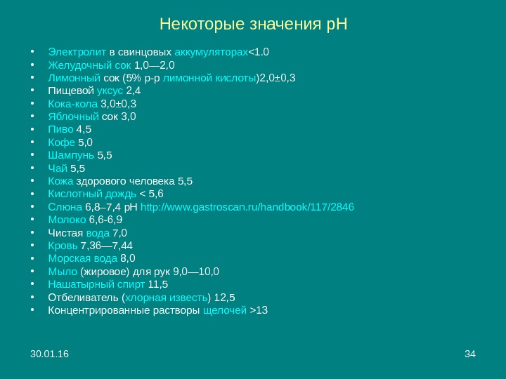
30. 01. 16 34 Некоторые значения p. H • Электролит в свинцовых аккумуляторах <1. 0 • Желудочный сок 1, 0— 2, 0 • Лимонный сок (5% р-р лимонной кислоты )2, 0± 0, 3 • Пищевой уксус 2, 4 • Кока-кола 3, 0± 0, 3 • Яблочный сок 3, 0 • Пиво 4, 5 • Кофе 5, 0 • Шампунь 5, 5 • Чай 5, 5 • Кожа здорового человека 5, 5 • Кислотный дождь
30. 01. 16 35 Sol-Gel Deposition Methods • A sol-gel process is a chemical reaction between solid particles in colloidal suspension within a fluid (a sol) to form a gelatinous network (a gel) that can be transformed to solid phase upon removal of the solvent. • Sol-gel is not a unique process, but rather represents a broad type of processes capable of forming glasses and ceramics in a multitude of shapes starting from basic chemical precursors.
30. 01. 16 36 • A widespread application of sol-gel processing is in the coating of surfaces with optical absorption or index-graded antireflective materials. • It has been used in research laboratories to deposit thick piezoelectric films on silicon substrates. • Silicon nitride, alumina, and piezoelectric PZT ( PZT , Lead Zirconate Titanate (piezoelectric ceramic material) can also be deposited by sol-gel methods.
30. 01. 16 37 Electroceramic properties • Being piezoelectric , it develops a voltage (or potential difference) across two of its faces when compressed (useful for sensor applications), or physically changes shape when an external electric field is applied (useful for actuator applications). The dielectric constant of PZT can range from 300 to 3850 depending upon orientation and doping. • Being pyroelectric , this material develops a voltage difference across two of its faces when it experiences a temperature change. As a result, it can be used as a heat sensor. • It is also ferroelectric , which means it has a spontaneous electric polarization ( electric dipole ) which can be reversed in the presence of an electric field. • The material features an extremely large dielectric constant at the morphotropic phase boundary (MPB) near x = 0. 52.
30. 01. 16 38 Varieties of PZTs • Сommonly studied chemical composition is Pb Zr 0. 52 Ti 0. 48 O 3. The increased piezoelectric response and poling (поляризационная) efficiency near to x = 0. 52 is due to the increased number of allowable (допустимый) domain states at the MPB. • At this boundary, the 6 possible domain states from the tetragonal phase and the 8 possible domain states from the rhombohedral phase are equally favorable energetically, thereby allowing a maximum 14 possible domain states. • Like structurally similar lead scandium tantalate and barium strontium titanate , PZT can be used for manufacture of uncooled staring array ( больших массивов) infrared imaging sensors for thermographic cameras. • Both thin film (usually obtained by chemical vapor deposition ) and bulk structures are used. The formula of the material used usually approaches Pb 1. 1 (Zr 0. 3 Ti 0. 7 )O 3 (called PZT 30/70). • Its properties may be modified by doping it with lanthanum , resulting in lanthanum-doped lead zirconate titanate ( PLZT , also called lead lanthanum zirconate titanate ), with formula Pb 0. 83 La 0. 17 (Zr 0. 3 Ti 0. 7 ) 0. 9575 O 3 (PLZT 17/30/70).
30. 01. 16 39 • A sol-gel process starts by dissolving appropriate chemical precursors in a liquid to form a sol (see Figure 3. 18). • After a time the sol goes through its gel point, the point at which the sol undergoes polymerization, to change it from a viscous liquid state to a gelatinous network. • Both sol formation and gelation are low-temperature steps. • The gel is then formed into a solid shape (e. g. , fiber or lens) or applied as a film coating on a substrate by spinning, dipping, or spraying. •
30. 01. 16 40 For example, TEOS in water can be converted into a silica gel by hydrolysis ( Гидр лизоо (от др. -греч. — разложение) — один из видов химических реакций сольволиза , где при взаимодействии веществ с водой происходит разложение исходного вещества с образованием новых соединений ) and condensation using hydrochloric acid as a catalyst. Drying and sintering at an elevated temperature (200°– 600°C) results in the transition of the gel to glass and then densification to silicon dioxide.
30. 01. 16 41 • Silica gel is a granular , vitreous (стекловидный) , porous form of silicon dioxide made synthetically from sodium silicate. • Silica gel is tough ( плотный ) and hard; it is more solid than common household gels like gelatin or agar. • It is a naturally occurring mineral that is purified and processed into either granular or beaded form. As a desiccant ( осушитель ) , it has an average pore size of 2. 4 nanometers and has a strong affinity for water molecules. • Silica gel is most commonly encountered in everyday life as beads in a small (typically 2 x 3 cm) paper packet. In this form, it is used as a desiccant ( осушитель ) to control local humidity to avoid spoilage ( порча) or degradation of some goods. Because of poisonous dopants and their very high absorption of moisture, silica gel packets usually bear warnings for the user not to eat the contents. ( Нельзя есть содержимое пакета с силикагелем).
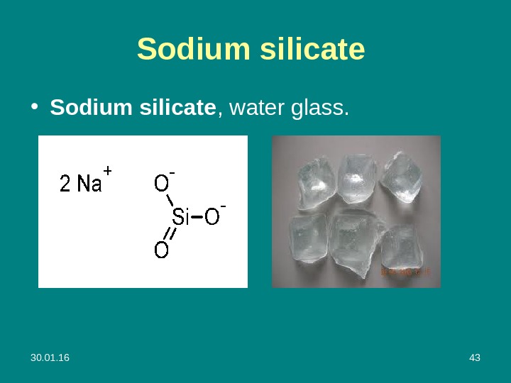
30. 01. 16 42 • Sodium silicate is the common name for a compound sodium metasilicate, Na 2 Si. O 3 , also known as waterglass or liquid glass. It is available in aqueous solution and in solid form and is used in cements, passive fire protection, refractories (огнеупорный материал) , textile and lumber processing ( деревообработка) , an d automobiles. • Sodium carbonate and silicon dioxide react when molten to form sodium silicate and carbon dioxide: Na 2 CO 3 + Si. O 2 → Na 2 Si. O 3 + CO
30. 01. 16 43 Sodium silicate • Sodium silicate , water glass.