
30. 01. 16 1 Electroplating and Molding


processes_for_micromachining-lecture_5.ppt
- Размер: 1.6 Mегабайта
- Количество слайдов: 72
Описание презентации 30. 01. 16 1 Electroplating and Molding по слайдам
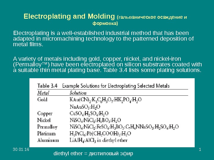
30. 01. 16 1 Electroplating and Molding (гальваническое осаждение и формовка) Electroplating is a well-established industrial method that has been adapted in micromachining technology to the patterned deposition of metal films. A variety of metals including gold, copper, nickel, and nickel-iron (Permalloy™) have been electroplated on silicon substrates coated with a suitable thin metal plating base. Table 3. 4 lists some plating solutions. diethyl ether = диэтиловый эфир
30. 01. 16 2 • Electroplated MEMS structures can take the shape of the underlying substrate and a photoresist mold. • First, a conducting seed layer (e. g. , of gold or nickel) is deposited on the substrate. In the simplest approach, thick (5 — to 100 -µm) resist is then deposited and patterned using optical lithography (see Figure 3. 19). • The largest aspect ratio achievable with optical lithography is approximately three , limited by resolution and depth of focus. • In LIGA , optical lithography is replaced with x-ray lithography to define very high aspect ratio features (>100) in very thick (up to 1, 000 µm) poly(methylmethacrylate) (PMMA) , the material on which Plexiglas® is based. • The desired metal is then plated. • Finally, the resist and possibly the seed layer outside the plated areas are stripped off ( удаляется).
30. 01.
30. 01.
30. 01. 16 5 • The process may be stopped at this point with a metal microstructure suitable for some purposes. Alternatively, the metal can be used as a mold for plastic parts (the “A” in LIGA). • Precision gears and other microstructures have been fabricated using LIGA, but the method is considered expensive because of the requirement to use collimated x-ray irradiation available only from synchrotrons. • Mold formation using optical lithography is often called “poor man’s LIGA. ” Guckel provides additional details on the molding of high aspect ratio structures fabricated with x-ray lithography. • In a variation known as electroforming, the plated metal is peeled off of the substrate and is the useful structure. • Examples of electroformed products are electric shaver screens ( сетки электробритв) and some ink-jet heads.
30. 01.
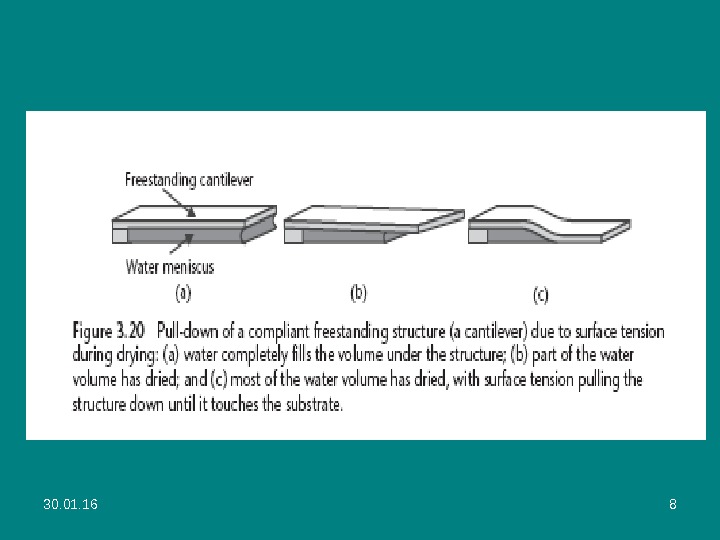
30. 01. 16 7 Supercritical Drying • The final step of micromachining processes is the removal of a sacrificial layer (e. g. , using hydrofluoric acid to etch 1 µm of silicon dioxide from under a polysilicon beam). • After rinsing, the water must be dried from the wafer. If a freestanding structure overhangs the substrate, surface tension forms a meniscus of water between the two (see Figure 3. 20). • As the water dries, its volume (and hence thickness) decreases. • If the structure is compliant, as is usually the case in surface micromachining, it is pulled down, contacting the substrate. • If a sufficiently large, smooth area of the structure makes contact, it can stick, which is known as stiction in the micromachining community. • Such stuck structures can often be freed by pushing with a probe tip , but this is hardly suitable for production.
30. 01.
30. 01. 16 9 • A solution to avoid stiction after release is supercritical drying, also known as critical-point drying. • In this process, the wafer is moved without drying into methanol, which is miscible (смешивается) with the small amount of water left on the wafer during transfer. • The wafer is then placed in a pressure chamber, covered by methanol. • Liquid carbon dioxide , which is miscible (смешивается) with methanol, is flowed into the chamber at a pressure of about 7. 5– 9 MPa as the methanol/carbon dioxide mixture is drained out (высушивается) of the bottom.
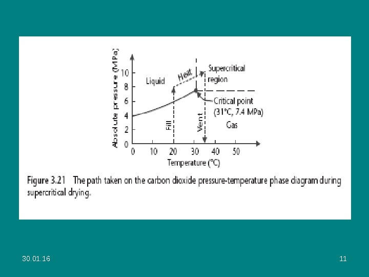
30. 01. 16 10 • After a few minutes, only carbon dioxide is left in the chamber. • The chamber is then heated from room temperature (near 20°C) to about 35°C, which also increases the pressure (see Figure 3. 21). • The carbon dioxide has now surpassed the critical point [31. 1°C, 7. 39 MPa] and is in the supercritical region, in which liquid and gas are indistinguishable. • Finally, the carbon dioxide is vented off. • As the pressure drops, the carbon dioxide in the chamber transitions from a supercritical fluid to a gas with only one phase ever being present, thus preventing the formation of a meniscus and the corresponding stiction. • Finally, the dried wafer is removed from the chamber.
30. 01.
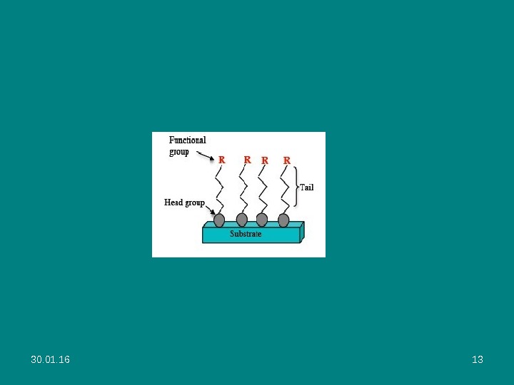
30. 01. 16 12 Self-Assembled Monolayers • The stiction problem during drying can also be avoided if a hydrophobic layer is coated onto the structure. • One method of doing this is the application of a self-assembled monolayer (SAM). • The SAM precursors used for this application are straight-chain hydrocarbons , such as octadecyltrichlorosilane (OTS, CH 3 (CH 2 )17 Si. Cl 3 ) , with a chemical group at one end that adheres to silicon, silicon-dioxide, and silicon-nitride surfaces. • Octadecyltrichlorosilane is an amphiphilic molecule consisting of a long-chain alkyl group (C 18 H 37 –) and a polar head group (Si. Cl 3 –), which forms Self assembled monolayers (SAMs) on various oxidic substrates.
30. 01.
30. 01. 16 14 Colour code Carbon, C: grey-black ; Hydrogen, H: white ; Chlorine, Cl: green ; Silicon, Si: turqouise-grey These head groups naturally pack tightly (накрепко) onto the surface and crosslink, leaving the tails sticking straight up away from the surface. The coating self-limits at one molecule of thickness and is hydrophobic (толщина слоя равна длине молекулы). In a SAM-coating process, the structures are released and rinsed in water as usual, then soaked (вымаивать) in a solvent (выдерживаются в растворе смешиваемым с водой) miscible with water.
30. 01. 16 15 • The wafer may be moved to an intermediate solvent compatible with the first solvent and the subsequent SAM solvent. ( Пластины могут быть перемещены в промежуточный растворитель, совместимый с первым растворителем и последующий SAM растворитель. ) • The wafer is then placed in a solution containing the SAM precursor and held for a few minutes, during which the coating occurs. • Finally, it is rinsed and dried, which may be done on a hot plate or under a heat lamp. • Due to the hydrophobicity of the SAM-coated surface, the contact angle changes, and the water does not pull compliant structures down to the substrate. ( В связи с гидрофобностью SAM-покрытия, изменяется угол смачивания, и вода не притягивает верхние структуры до подложки). • An added benefit is that if the structure ever does touch down during operation, it will not stick, as it might otherwise do without the coating. (Дополнительным преимуществом является то, что если структура все же соприкаснется с подложкой во время процесса, она не будет удерживаться, в то время как без покрытия структура будет удерживаться. ) • SAM coatings have also been studied as a dry lubricant and found to prolong the life of micromachined parts sliding in contact, eventually wearing out. (SAM покрытия изучались также в качестве сухой смазки и нашли применение для продления срока службы микромеханических частей устройств, поскольку износ становится меньше. ) • SAMs decompose at high temperatures (~350°C).
30. 01. 16 16 SU-8 Photosensitive Epoxy • Epoxies have been in use for decades for joining sections of material together and as a structural component of composites. • Some epoxies are formulated to be sensitive to ultraviolet light, allowing photolithographic patterning. SU-8 is a negative-acting photosensitive epoxy intended for use in fabricating microstructures. • Originally developed by International Business Machines Corp. , it is commercially produced under license by two companies, Micro. Chem Corp. of Newton, Massachusetts, and SOTEC Microsystems of Renens, Switzerland.
30. 01. 16 17 • SU-8 is spun onto a substrate in the same manner as photoresist. • Different viscosities and a range of spin speeds yield thicknesses from 0. 5 to over 250 µm with a single coating. • Multiple spins have been used to coat up to 1 mm. • The epoxy is then exposed, typically with a standard contact lithography system in the near UV (350– 400 nm), but x-rays or an electron beam may also be used. • At wavelengths longer than 350 nm, SU-8 has little absorption, allowing exposure through the thickness of much thicker layers than are typically used for traditional photoresist. (При длинах волн более 350 нм, SU -8 имеет мало поглощения, что позволяет экспонировать более толстые слои, чем обычно используются для традиционных фоторезистов).
30. 01. 16 18 • During exposure, a strong acid is generated where exposed. • During the postexposure bake, the acid initiates thermally driven crosslinking. • Immersion in a developer then removes the SU-8 that is not crosslinked. At this point, the remaining material is suitable for many applications, but a hard bake may be performed to promote further crosslinking.
30. 01. 16 19 • SU-8 structures are the same thickness as the original spin. Aspect ratios (ratio of epoxy height to width) of 20: 1 are regularly produced. • The cured material (затвердевший материал) is resistant to most chemicals and is thermally stable. • SU-8 has been used to form microfluidic channels and optical waveguides. • It has also been used as the mask for thick electroplating, although stripping (удаление) the SU-8 is much more difficult than stripping (удаление) photoresist.
30. 01. 16 20 Photosensitive Glass • Positive-acting photosensitive glass wafers are made commercially under the trade name FORTURAN® by Schott Glas of Mainz, Germany, and processed by Mikroglas Technik AG of Mainz, Germany. • FORTURAN is a lithium aluminum silicate glass with small amounts of cerium and silver ions. • The full thickness of the glass is exposed with ultraviolet light through a mask, causing the silver ions to form atoms (Облучение заставляет ионы серебра обращаться в атомы). • Annealing causes Ag- atoms to aggregate into microscopic particles, which then serve as nucleation sites for lithium metasilicate crystals. The crystallized volumes are etched relatively rapidly in HF , leaving holes through the wafer. (Отжиг способствует объединению Ag-атомов в микроскопические частицы, которые затем служат в качестве центров кристаллизации для кристаллов метасиликата лития. Кристаллизуемые объемы травятся относительно быстро в HF, таким образом получаются отверстия в стеклянной пластине).
30. 01. 16 21 • Up to 14 patterned or unpatterned glass wafers can be thermally bonded together, creating complex systems of channels suitable for microfluidic applications. • Substrates 150 to 1, 500 µm thick can be processed. The smallest hole that can be formed in a 400 -µm wafer is 60 µm, for an aspect ratio of (7) seven, with a 1. 5 -µm tolerance. • Sidewalls are within 2 o of vertical.
30. 01. 16 22 EFAB is the trade name for an E lectrochemical FAB rication surface micromachining • In the EFAB process, three-dimensional structures are created by multilayer depositions of patterned metals. • Photolithographic techniques are used to deposit a patterned layer of metal (see Figure 3. 22). • While the details of the process are proprietary, one could accomplish such a structure by electroplating through patterned photoresist. (Детали этого процесса являются собственностью компании, но можно представить процесс, как показано на рисунке). • Next, a blanket deposition of a second metal is performed, which fills in the spaces left from the patterned deposition, as well as coating the first metal.
30. 01.
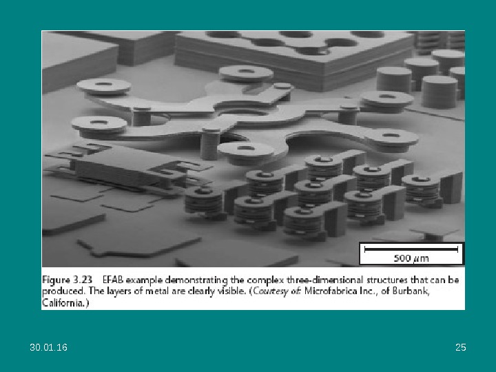
30. 01. 16 24 • The structure is then planarized, leaving the entire substrate covered by patterns of the two metals, all the same thickness. • These three steps are then repeated with different masks as many times as necessary to build the desired structure. • The definition of each layer is arbitrary with respect to the previous layer. • Finally, one of the metals is selectively etched as a sacrificial layer, leaving behind the other as a structural layer (see Figure 3. 23).
30. 01.
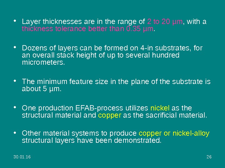
30. 01. 16 26 • Layer thicknesses are in the range of 2 to 20 µm , with a thickness tolerance better than 0. 35 µm. • Dozens of layers can be formed on 4 -in substrates, for an overall stack height of up to several hundred micrometers. • The minimum feature size in the plane of the substrate is about 5 µm. • One production EFAB-process utilizes nickel as the structural material and copper as the sacrificial material. • Other material systems to produce copper or nickel-alloy structural layers have been demonstrated.
30. 01. 16 27 Nonlithographic Microfabrication Technologies Ultraprecision Mechanical Machining • Cutting tools such as mills ( дробление), lathes (обраб отка на токарном станке) , and drills using a specially hardened cutting edge have been in use for the production of macroscopic parts for over a century. • Using modern computer-numerical-controlled (CNC) machines with sharply tipped diamond-cutting tools, many metals and even silicon have been milled to a desired shape, with some features smaller than 10 µm. •
30. 01. 16 28 • Many of these shapes, such as retrograde undercuts with flat sidewalls, cannot be formed using lithographic methods. • Resolution of about 0. 5 µm can be achieved, with surface roughnesses on the order of 10 nm. • Example applications include optical mirrors and computer harddrive disks.
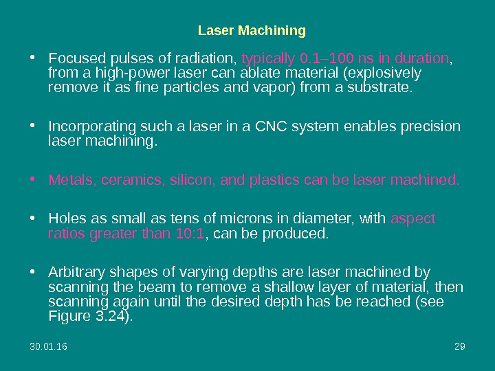
30. 01. 16 29 Laser Machining • Focused pulses of radiation, typically 0. 1– 100 ns in duration , from a high-power laser can ablate material (explosively remove it as fine particles and vapor) from a substrate. • Incorporating such a laser in a CNC system enables precision laser machining. • Metals, ceramics, silicon, and plastics can be laser machined. • Holes as small as tens of microns in diameter, with aspect ratios greater than 10: 1 , can be produced. • Arbitrary shapes of varying depths are laser machined by scanning the beam to remove a shallow layer of material, then scanning again until the desired depth has be reached (see Figure 3. 24).
30. 01. 16 30 • Laser machining can be used to create perforations in silicon wafers for subsequent cleaving to form individual chips, as well as simply cutting though the full wafer thickness. • Laser machining is most often a serial process, but with mask-projection techniques, it becomes a parallel process. • It has successfully competed with KOH etching and with electroplating in the production of ink-jet nozzles. • Due to its speed, low cost, and rapid turn-around time, laser machining is one of the preferred methods of creating trenches and cuts in plastics.
30. 01.
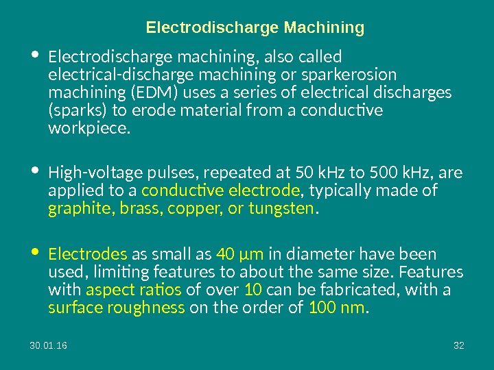
30. 01. 16 32 Electrodischarge Machining • Electrodischarge machining, also called electrical-discharge machining or sparkerosion machining (EDM) uses a series of electrical discharges (sparks) to erode material from a conductive workpiece. • High-voltage pulses, repeated at 50 k. Hz to 500 k. Hz, are applied to a conductive electrode , typically made of graphite, brass, copper, or tungsten. • Electrodes as small as 40 µm in diameter have been used, limiting features to about the same size. Features with aspect ratios of over 10 can be fabricated, with a surface roughness on the order of 100 nm.
30. 01. 16 33 • Each discharge removes a small volume of material, typically in the range of 10 3 to 10 5 µm 3 , from the workpiec e ( обрабатываемая деталь ). • EDM is performed in a dielectric liquid such as mineral oil. • Due to heating, a gas bubble is formed during each voltage pulse. • After the pulse, the bubble collapses, flushing away debris from the blank and electrode. ( После импульса, пузырек газа лопается, удаляя остатки материала от обрабатываемой детали и электрода). • EDM has been used to create the tooling for molds and stamping tools, as well as final products such as nozzles and holes in microneedles.
30. 01. 16 34 Screen Printing • Screen printing, also known as silk screening. • In electronics, it has long been used in the production of ceramic packages and more recently for large flat-panel displays. • In a parallel process, many ceramic packages are processed together on a single plate, then separated near the end of the process. • A wide variety of materials , including metals and ceramics, can be applied using screen printing. • It does not have same resolution as photolithography , but is cost effective and is readily applied to large substrates.
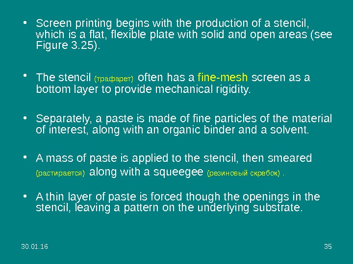
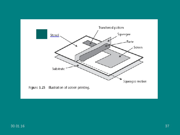
30. 01. 16 35 • Screen printing begins with the production of a stencil, which is a flat, flexible plate with solid and open areas (see Figure 3. 25). • The stencil (трафарет) often has a fine-mesh screen as a bottom layer to provide mechanical rigidity. • Separately, a paste is made of fine particles of the material of interest, along with an organic binder and a solvent. • A mass of paste is applied to the stencil, then smeared (растирается) along with a squeegee (резиновый скребок). • A thin layer of paste is forced though the openings in the stencil, leaving a pattern on the underlying substrate.
30. 01. 16 36 • Drying evaporates the solvent. • Firing burns off the organic binder and sinters the remaining metal or ceramic into a solid, resulting in a known amount of shrinkage. (При выжигании органических связующих оставшиеся металлические или керамические частички спекаются в твердое состояние, в результате происходит усадка размеров). • Metal lines with 125 -µm lines and spaces are made in the production of ceramic packaging, with 30 -µm features demonstrated. • Film thicknesses after firing range from roughly 10 to 200 µm. • Multiple layers of different materials can be stacked.
30. 01.
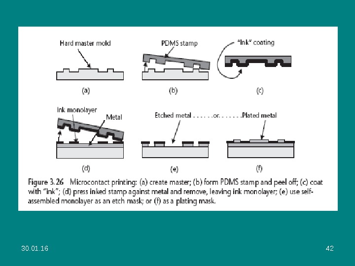
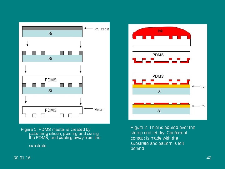
30. 01. 16 38 Microcontact Printing/Soft Lithography • Microcontact printing, a microscale form of ink printing also called soft lithography. • It enables low-cost production of submicrometer patterns and has been studied as an alternative to conventional photolithography, but is not presently a product fabrication method. • The process begins with the production of the original, hard, three-dimensional master pattern (see Figure 3. 26), which can involve conventional photolithography and etching, electron-beam lithography, laser scribing, diamond scribing, or any other suitable method. • A mold of an elastomer, usually poly(dimethylsiloxane) (PDMS ), is made against the master, then peeled off to create a stamp with raised patterns.
30. 01. 16 39 • An “ink, ” a liquid solution typically of an alkanethiol (a hydrocarbon chain ending in a thiol, an –SH group) such as hexadecanethiol, is poured onto the PDMS stamp and dried. • The inked stamp is then held against a substrate coated with gold, silver, or copper, then removed. • The thiol end of each “ink” molecule bonds to the metal, forming a densely packed, single-molecule-thick coating of hexadecanethiol where the raised areas of the stamp were. • Such SAM coatings can be envisioned as similar to turf with dense blades of grass. Такие SAM покрытия похожи на дерн плотно покрытый упорядоченными травинками. • Once the SAM coating is in place, it can be used as an etch mask for the metal. • The metal can then be used as an etch mask for the underlying substrate, such as silicon.
30. 01. 16 40 • Several variations on this scheme may be performed. In one, a metal catalyst “ink” is stamped on the substrate, which is then used for the selective plating of copper. • In another, proteins or other biological molecules are coated onto a flat stamp. • A patterned PDMS layer contacts the flat stamp and is removed, taking the protein with it where contact occurred. The flat stamp is then held against a substrate, transferring the protein pattern. • Features smaller than 0. 1 μm have been made using microcontact printing. • The best alignment accuracy of a second pattern, however, is at present about 20 μm, so most soft lithography applications have used a single step.
30. 01. 16 41 • In organic chemistry, a thiol is an organosulfur compound that contains a carbon-bonded sulfhydryl (–C–SH or R–SH) group (where R represents an alkane, alkene, or other carbon-containing group of atoms). Thiols are the sulfur analogue of alcohols (that is, sulfur takes the place of oxygen in the hydroxyl group of an alcohol), and the word is a portmanteau of «thio» + «alcohol, » with the first word deriving from. Greek θε ον («thion») = «sulfur». The –SH ῖ functional group itself is referred to as either a thiol group or a sulfhydryl group. • Many thiols have strong odors resembling that of garlic. Thiols are used as odorants to assist in the detection of natural gas (which in pure form is odorless), and the «smell of natural gas» is due to the smell of the thiol used as the odorant. Thiol with a blue highlighted sulfhydryl group.
30. 01.
30. 01. 16 43 Figure 1: PDMS master is created by patterning silicon, pouring and curing the PDMS, and peeling away fro m the substrate Figure 2: Thiol is poured over the stamp and let dry. Conformal contact is made with the substrate and pattern is left behind.
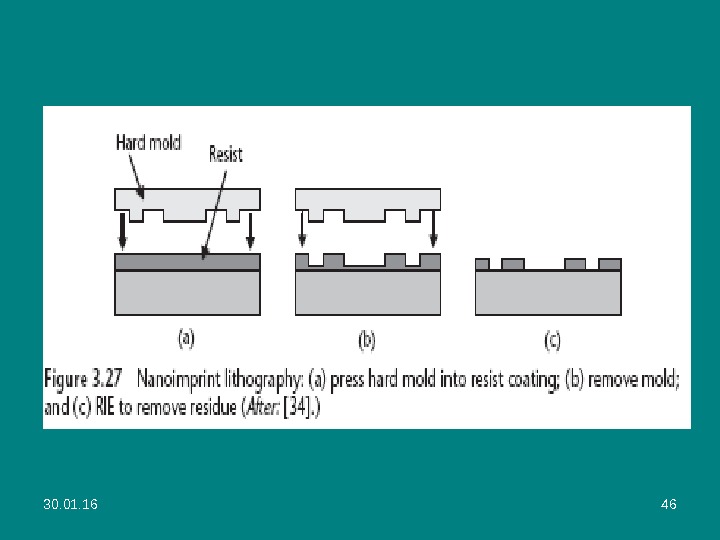
30. 01. 16 44 • As with microcontact printing, nanoimprint lithography has the goal of generating submicrometer features at low cost and high throughput and is not a production p rocess. • It starts with a mold of etched silicon, silicon dioxide, or other hard material created using optical or electron-beam lithography (see Figure 3. 27). • Separately, a substrate is coated with a 50 — to 250 -nm resist layer such as PMMA o r a more conventional novolak-resin-based resist, which does not need to be photosensitive. • The resist is heated above its glass transition temperature so that it flows easily under pressure. Nanoimprint Lithography
30. 01. 16 45 • The mold is then pressed into the resist, which flows to the sides of the high points in the mold. • The mold is removed, leaving an unintentional ( случайный ) residue of resist where the mold high points were. • This residue is stripped using vertical RIE. • At this point, the resist pattern can be used like conventional photoresist in an etch, liftoff, or plating process. • Features 25 nm wide with smooth sidewalls have been demonstrated. • Alignment accuracy of a second nanoimprint step is likely to be many micrometers, but the technique has been combined with optical lithography to fabricate devices with several layers.
30. 01.
30. 01.
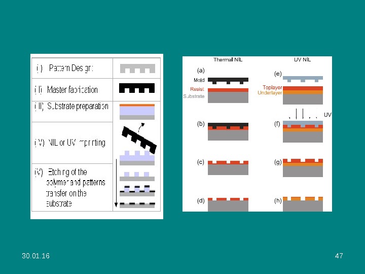
30. 01. 16 48 Thermoplastic nanoimprint lithography • Thermoplastic nanoimprint lithography (T-NIL) is the earliest nanoimprint lithography developed by Prof. Stephen Chou’s group. • In a standard T-NIL process, a thin layer of imprint resist (thermoplastic polymer) is spin coated onto the sample substrate. • Then the mold, which has predefined topological patterns, is brought into contact with the sample and they are pressed together under certain pressure. • When heated up above the glass transition temperature of the polymer, the pattern on the mold is pressed into the softened polymer film. • After being cooled down, the mold is separated from the sample and the pattern resist is left on the substrate. • A pattern transfer process (reactive ion etching, normally) can be used to transfer the pattern in the resist to the underneath substrate.
30. 01. 16 49 • Alternatively, cold welding between two metal surfaces could also transfer low dimensional nanostructured metal without heating (especially for critical sizes less than ~10 nm), . • Three-dimensional structures can be fabricated by repeating this procedure. The cold welding approach has the advantage of reducing surface contact contamination or defect due to no heating process, which is a main problem in the latest development and fabrication of organic electronic devices as well as novel solar cells.
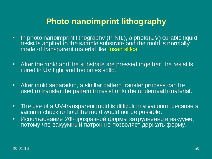
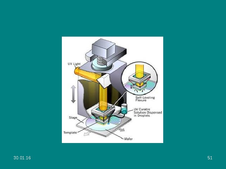
30. 01. 16 50 Photo nanoimprint lithography • In photo nanoimprint lithography (P-NIL), a photo(UV) curable liquid resist is applied to the sample substrate and the mold is normally made of transparent material like fused silica. • After the mold and the substrate are pressed together, the resist is cured in UV light and becomes solid. • After mold separation, a similar pattern transfer process can be used to transfer the pattern in resist onto the underneath material. • The use of a UV-transparent mold is difficult in a vacuum, because a vacuum chuck to hold the mold would not be possible. • Использование УФ-прозрачной формы затрудненно в вакууме, потому что вакуумный патрон не позволяет держать форму.
30. 01.
30. 01. 16 52 Ultrasonic Machining • In ultrasonic machining, also known as ultrasonic impact grinding, a transducer vibrates a tool at high frequency (20– 100 k. Hz). The tip of the tool is pushed against the workpiece as a slurry of water or oil and abrasive particles, such as boron carbide, aluminum oxide, or silicon carbide , is flushed across the surface. • There are several mechanisms for removal of material: The tool vibration directly hammers particles into the surface, as well as imparting a high velocity to other particles, both of which chip away at the workpiece. Cavitation erosion and chemical action can also contribute. The microscopic chips are carried away by the slurry. • As the tool moves slowly into the workpiece, a hole with vertical sidewalls is created. • An array of tips can drill many holes at the same time.
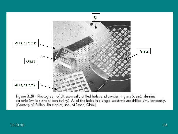
30. 01. 16 53 • Figure 3. 28 shows examples in several materials. The hole shape matches that of the tool and can be round, square, or other. • Ultrasonic machining can be performed on hard, brittle materials (with a Knoop hardness above about 400) such as glasses, ceramics, diamond, and silicon. • The minimum hole diameter is about 150 µm. • At the other extreme, holes over 100 mm have been machined. • For small holes, the maximum aspect ratio is about five (5 ), increasing to over 15 for holes several millimeters in diameter. • With tolerancing, the size accuracy of 1 -mm holes is typically ± 50 µm , improving to ± 25 µm for larger holes. Hole depth can be over 10 mm.
30. 01. 16 54 Al 2 O 3 ceramic Glass Al 2 O 3 ceramic Si
30. 01. 16 55 Combining the Tools—Examples of Commercial Processes. Polysilicon Surface Micromachining. • The polysilicon is deposited using LPCVD, followed by a high-temperature anneal (>900 o C) to relieve mechanical stress. • The silicon dioxide is deposited using LPCVD or PECVD and is often doped with phosphorus [phosilicate glass (PSG)] to increase the etch rate in hydrofluoric acid. • In the Sandia process, the polysilicon and silicon dioxide layers are each 2 µm thick. • By contrast, Robert Bosch uses a process with 10 -µm -thick polysilicon grown by epitaxy over silicon dioxide.
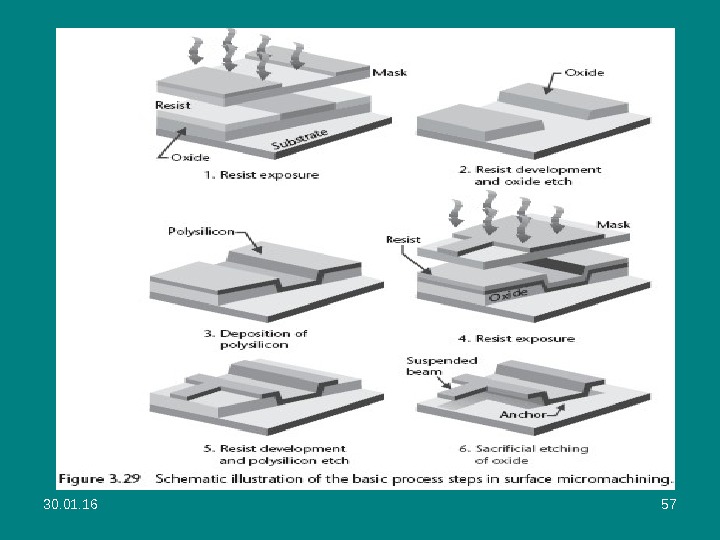
30. 01. 16 56 • Each of the layers in the stack is lithographically patterned and etched before the next layer is deposited in order to form the appropriate shapes and to make provisions for anchor points to the substrate (see Figure 3. 29). • The final release step consists of etching the silicon dioxide (the sacrificial term) in a HF- solution to free the polysilicon plates and beams, thus allowing motion in the plane of and perpendicular to the substrate. • Small holes are usually added to large plates to allow the sacrificial etchant access for faster release. • To avoid sticking of compliant structures when drying the wafer, supercritical drying or a SAM ( self-assembled monolayer ) is often used.
30. 01.
30. 01. 16 58 • Gears, micromotors, beams, simple as well as hinged plates, and a number of other structures have been demonstrated, though ( хотя ) primarily accelerometers and yaw-rate sensors (сенсоры угловой скорости ) are currently in high-volume production. • Surface micromachining offers significant flexibility to fabricate planar structures one layer at a time, but t heir thinness limits the applications to those benefiting from essentially two — dimensional forms. Поверхностная микрообработка позволяет сделать широкий выбор в изготовлении структур в плоскости, но их утоньшение ограничивает приложения для 2 D- структур. • Polysilicon is a useful structural material because integrated circuit processes already exist for depositing and etching it and because its thermal coefficient of expansion is well matched to that of the silicon substrate.
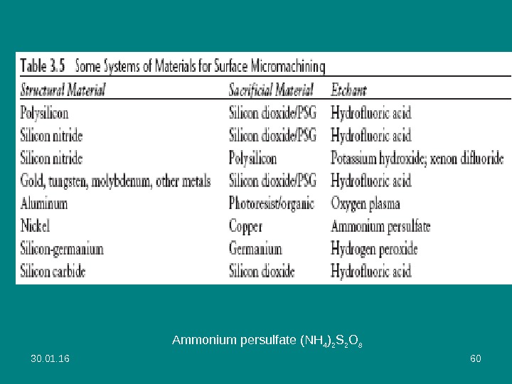
30. 01. 16 59 • S urface micromachining is not limited to the materials just described. Many systems of structural layer, sacrificial layer, and etchant have been used, as shown in Table 3. 5. • The etchant must etch the sacrificial layer at a useful rate, while having little or no impact on the structural layer. • Reasons for selecting materials other than polysilicon include the need for higher electrical conductivity, higher optical reflectivity, and lower deposition temperature for compatibility with CMOS circuitry that is already on the wafer. • For example, Texas Instruments’ Digital Mirror Device™ (DMD™) display technology uses a surface-micromachined device with aluminum as its structural element and an organic polymer as a sacrificial layer.
30. 01. 16 60 Ammonium persulfate (NH 4 ) 2 S 2 O
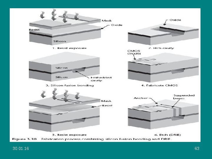
30. 01. 16 61 Combining Silicon Fusion Bonding with Reactive Ion Etching • The silicon fusion bonding with reactive ion etching (SFB-DRIE) process involves the formation of tall structures in crystalline silicon to overcome thinness limitation of surface micromachining. (Сочетание процесса сращивания пластин кремния с реактивным ионным травлением (SFB-DRIE) позволяет формировать высокие конструкции в кристаллическом кремнии, чтобы преодолеть ограничение по толщине). • Instead of depositing thin polysilicon layers, crystalline silicon substrates are fusion bonded to each other in a stack. • Each substrate is polished down to a desired thickness, then patterned and etched before the next one is bonded. • An optional intermediate silicon dioxide between the silicon substrates is not a sacrificial layer but is rather for electrical and thermal insulation. Дополнительный промежуточный диоксид кремния между кремниевыми пластинами не является жертвенным слоем, а скорее электрическим и тепловым изолятором. • The process allows the building of complex three-dimensional structures one thick layer at a time.
30. 01. 16 62 • The basic process flow begins by etching a cavity in a first wafer, referred to as the handle wafer (see Figure 3. 30). • A second wafer is silicon fusion bonded on. • An optional grind and polish step reduces the thickness of the bonded wafer to any desired value. • CMOS electronic circuits can then be integrated on the top surface of the bonded stack without affecting any of its mechanical properties. • Finally, a DRIE step determines the shape of the microstructures and mechanically releases them as soon as the etch reaches the embedded cavity. • This cavity takes the role of the sacrificial layer in surface micromachining and ensures that the micromechanical structures are free to move except at well-defined anchor points.
30. 01.
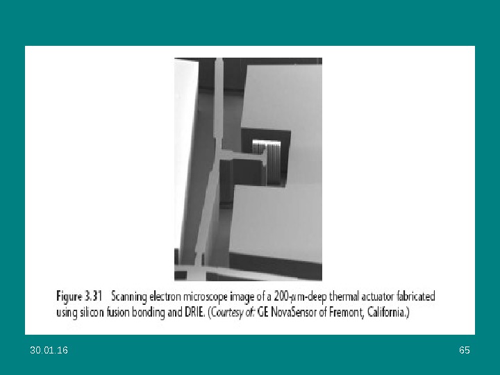
30. 01. 16 64 • The high aspect ratio and depth available using the SFB-DRIE process add new dimensions to the design and fabrication of complex three-dimensional structures (see Figure 3. 31). • A range of new applications, including those integrating fluid flow functions such as valving and pumping, can be addressed with this process. • Robust (надежный) thermal actuators made of crystalline silicon are also feasible with an available output force approaching one newton. • This process is now a manufacturing platform at GE Nova. Sensor of Fremont, California.
30. 01.
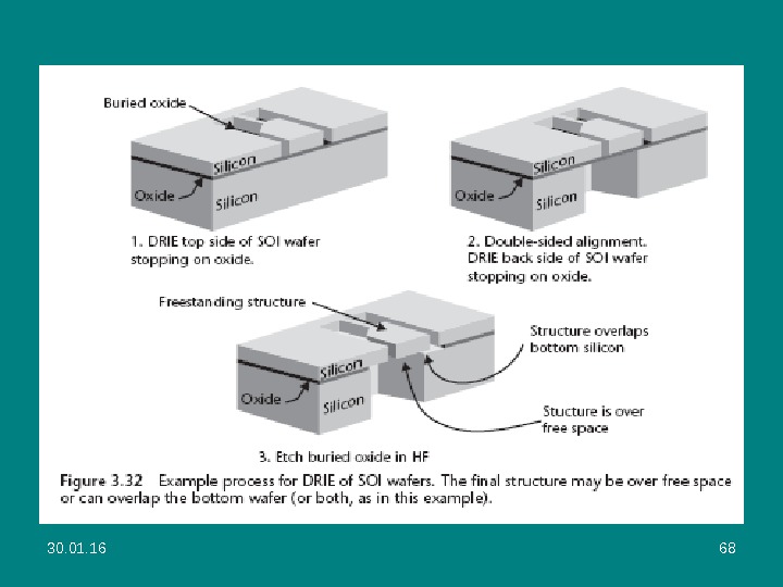
30. 01. 16 66 DRIE of SOI Wafers • The availability of double-sided aligners, DRIE tools, and SOI wafers led to a relatively simple process for fabricating three-dimensional microstructures that became popular in the late 1990 s. • The process begins with DRIE of the thinner top layer of an SOI wafer to form the desired structure (see Figure 3. 32). • The etch stops with high selectivity on the buried oxide layer. • If undercut of the silicon at the oxide interface control is not desired, the specialized stop-on-oxide recipe can be used. • A large area of the back side, corresponding to the structure on the front side, is etched to the buried oxide layer.
30. 01. 16 67 • Finally, the now-freestanding buried oxide is etched away, typically with hydrogen fluoride [hydrofluoric acid (HF)] vapor or a liquid HF solution, both of which selectively etch the oxide. • If liquid HF is used and the structure is fragile, it must be handled carefully to avoid breakage during etching, rinsing, and drying. • A variation on the process is to etch the device structure from the top, then release it by etching the underlying oxide, which may be as thick as 2 µm, in liquid HF. • If the structure is sufficiently stiff (жесткая), it can be dried without special handling. • If it is too compliant, critical-point drying can be used.
30. 01.
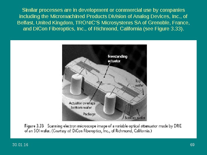
30. 01. 16 69 Similar processes are in development or commercial use by companies including thе Micromachined Products Division of Analog Devices, Inc. , of Belfast, United Kingdom, TRONIC’S Microsystems SA of Grenoble, France, and Di. Con Fiberoptics, Inc. , of Richmond, California (see Figure 3. 33).
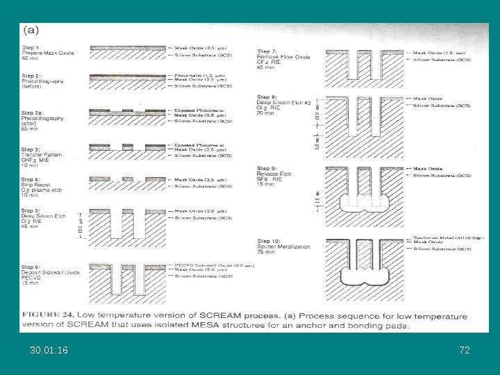
30. 01. 16 70 Single Crystal Reactive Etching and Metallization • The single-crystal reactive etching and metallization (SCREAM) process uses yet another approach to release crystalline microstructures. • Standard lithography and etching methods define trenches between 10 and 50 µm in depth, which are then coated on the top, sidewalls, and bottom with a conformal layer of PECVD silicon dioxide (see Figure 3. 34). • An anisotropic etch step selectively removes the protective oxide only at the bottom of the trench. • A subsequent plasma silicon etch extends the depth of the trench. A dry isotropic etch step using sulfur hexafluoride (SF 6 ) laterally etches the exposed sidewalls near the bottom of the trench, thus undercutting adjacent structures and mechanically releasing them. • Sputter deposition of aluminum provides the metal for electrical contacts and interconnects. • This process, known by its SCREAM acronym, was initially developed at Cornell University. Kionix, Inc. , of Ithaca, New York, uses a variation of SCREAM for the manufacture of accelerometers, micromirrors, and other devices.
30. 01.
30. 01.