
1 Notebook Power System Introduction & Troubleshooting Система


notebook_power_system_introduction_troubleshooting.ppt
- Размер: 875.5 Кб
- Количество слайдов: 42
Описание презентации 1 Notebook Power System Introduction & Troubleshooting Система по слайдам
1 Notebook Power System Introduction & Troubleshooting Система питания ноутбука Введение и устранение неисправностей PE Mike Lee 03/29/
2 Notebook Power System Introduction & Troubleshooting. Целевая аудитория • Все электротехники, такие как : • PE, TE, FAE, CSD Необходимые знания • Электронные схемы • Цифровые логические схемы • Использование мульти-метра Содержание курса • Система питания и последовательности • Поиск неисправностей • Выводы • Принцип передачи мощности ( ШИМ -Plus импульсной модуляции & LDO –Low Drop-Out regulator ) • Зарядное устройство После этого курса Вы будите • Уметь находить неисправности в цепях питания. Для кого эта презентация
3 Notebook Power System Introduction & Troubleshooting 1. 1 Введение в NB системы питания 1. 2 Последовательность питания и управления 2. 1 Блок-схема цепей питания 2. 2 NB power application 2. 3 Multi–power device 3. 1 No power debug notice & sequence 3. 2 DCBATOUT short( 短短 ) to GND 3. 2 S 5 Power No Good 3. 3 Power on logic No Good. План : 1. Архитектура цепей питания : 3. No power debug : 2. Введение в схему питания : План
4 Notebook Power System Introduction & Troubleshooting Как мы знаем, ноутбук питание обеспечивается адаптерами (19 V) или батарей (14. 8 V). Тем не менее, различные ( 短短 短 ) напряжения питания не подходят ( 短短 ) все устройства к каждому ноутбуку. Так ряд действий по передаче напряжения необходимы для питания всех устройств. (Могут возникнуть проблемы ( 短短 ) во время передачи напряжения. ) Как ноутбук портативный компьютер, экономя энергию также очень важно, когда система находится в режиме работы от батареи. В этом уроке, мы будем использовать схему питания Юхина внедрить систему питания ноутбука. • Foreword : Foreword
5 Notebook Power System Introduction & Troubleshooting 1. 1 NB (Yuhina) power system : AUX Power PWM Charger P-MOS SI 4425 PWM MAX 1999 PWM MAX 1715 AD+ BT+ N-MOS FD 9412 5 V_S 5 Max 1999_LDO 5 5 V_AUX_S 5 +5 V_UP_S 5 3 D 3 V_S 5 DCBATOUT N-MOS FD 9412 LDO G 913 C 5 V_S 3 3 D 3 V_S 3 5 V_S 0 3 D 3 V_LAN_S 5 1 D 5 V_S 5 2 D 5 V_S 3 2 D 5 V_S 0 LDO G 913 C 1 D 25 V_S 0 S 5 Power S 3 Power S 0 Power PWM MAX 1546 VCC_CORE_S 0 1 D 5 V_S 01 4 3 2 1 66 5 7 64 7 751. Power system architecture 1 of
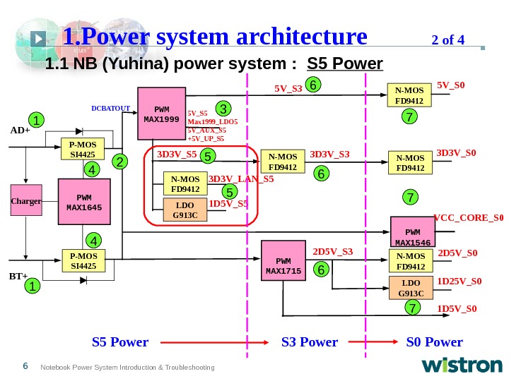
6 Notebook Power System Introduction & Troubleshooting 1. 1 NB (Yuhina) power system : S 5 Power PWM MAX 1645 Charger P-MOS SI 4425 PWM MAX 1999 PWM MAX 1715 AD+ BT+ N-MOS FD 9412 5 V_S 5 Max 1999_LDO 5 5 V_AUX_S 5 +5 V_UP_S 5 3 D 3 V_S 5 DCBATOUT N-MOS FD 9412 LDO G 913 C 5 V_S 3 3 D 3 V_S 3 5 V_S 0 3 D 3 V_LAN_S 5 1 D 5 V_S 5 2 D 5 V_S 3 2 D 5 V_S 0 LDO G 913 C 1 D 25 V_S 0 S 5 Power S 3 Power S 0 Power. PWM MAX 1546 VCC_CORE_S 0 1 D 5 V_S 01 4 3 2 1 66 5 7 64 7 751. Power system architecture 2 of
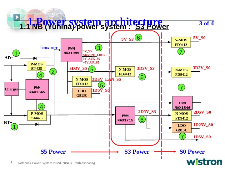
7 Notebook Power System Introduction & Troubleshooting 1. 1 NB (Yuhina) power system : S 3 Power PWM MAX 1645 Charger P-MOS SI 4425 PWM MAX 1999 PWM MAX 1715 AD+ N-MOS FD 9412 5 V_S 5 Max 1999_LDO 5 5 V_AUX_S 5 +5 V_UP_S 5 3 D 3 V_S 5 DCBATOUT N-MOS FD 9412 LDO G 913 C 5 V_S 3 3 D 3 V_S 3 5 V_S 0 3 D 3 V_LAN_S 5 1 D 5 V_S 5 2 D 5 V_S 3 2 D 5 V_S 0 LDO G 913 C 1 D 25 V_S 0 S 5 Power S 3 Power S 0 Power. PWM MAX 1546 1 D 5 V_S 01 4 3 2 1 66 5 7 64 7 75 BT+ 1. Power system architecture 3 of
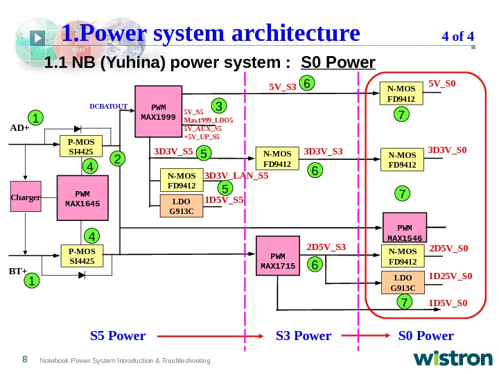
8 Notebook Power System Introduction & Troubleshooting PWM MAX 1645 Charger P-MOS SI 4425 PWM MAX 1999 PWM MAX 1715 AD+ N-MOS FD 9412 5 V_S 5 Max 1999_LDO 5 5 V_AUX_S 5 +5 V_UP_S 5 3 D 3 V_S 5 DCBATOUT N-MOS FD 9412 LDO G 913 C 5 V_S 3 3 D 3 V_S 3 5 V_S 0 3 D 3 V_LAN_S 5 1 D 5 V_S 5 2 D 5 V_S 3 2 D 5 V_S 0 LDO G 913 C 1 D 25 V_S 0 S 5 Power S 3 Power S 0 Power. PWM MAX 1546 1 D 5 V_S 01 4 3 2 1 66 5 7 64 7 75 BT+ 1. 1 NB (Yuhina) power system : S 0 Power 1. Power system architecture 4 of
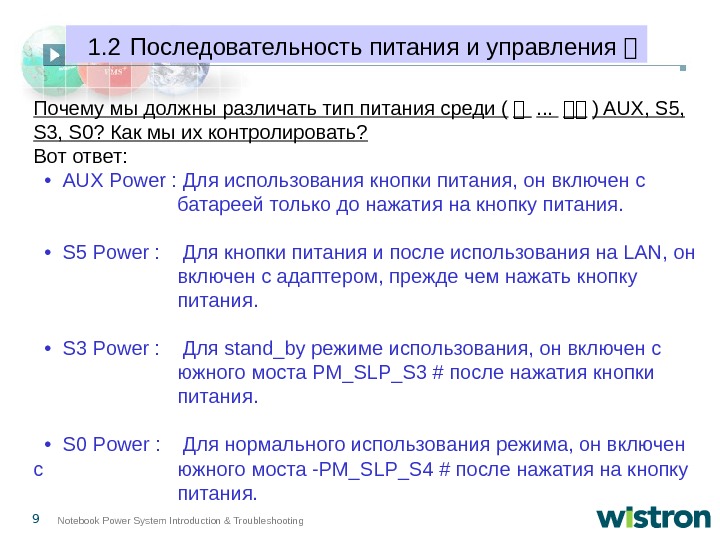
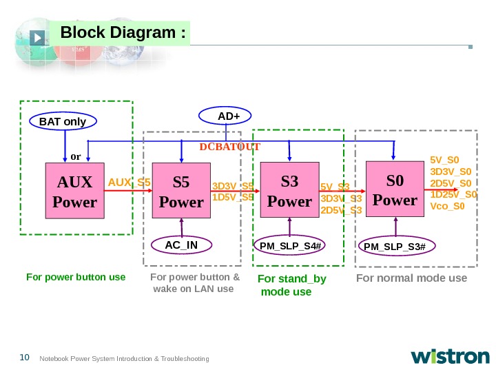
9 Notebook Power System Introduction & Troubleshooting. Почему мы должны различать тип питания среди ( 短 . . . 短短 ) AUX, S 5, S 3, S 0? Как мы их контролировать? Вот ответ: • AUX Power : Для использования кнопки питания, он включен с батареей только до нажатия на кнопку питания. • S 5 Power : Для кнопки питания и после использования на LAN, он включен с адаптером, прежде чем нажать кнопку питания. • S 3 Power : Для stand_by режиме использования, он включен с южного моста PM_SLP_S 3 # после нажатия кнопки питания. • S 0 Power : Для нормального использования режима, он включен с южного моста -PM_SLP_S 4 # после нажатия на кнопку питания. 1. 2 Последовательность питания и управления 短
10 Notebook Power System Introduction & Troubleshooting AUX Power S 5 Power S 3 Power S 0 Power. BAT only AD+ or AUX_S 5 3 D 3 V_S 5 1 D 5 V_S 5 DCBATOUT AC_IN PM_SLP_S 4# PM_SLP_S 3#5 V_S 3 3 D 3 V_S 3 2 D 5 V_S 3 5 V_S 0 3 D 3 V_S 0 2 D 5 V_S 0 1 D 25 V_S 0 Vco_S 0 For power button use For stand_by mode use For normal mode use. For power button & wake on LAN use. Block Diagram :
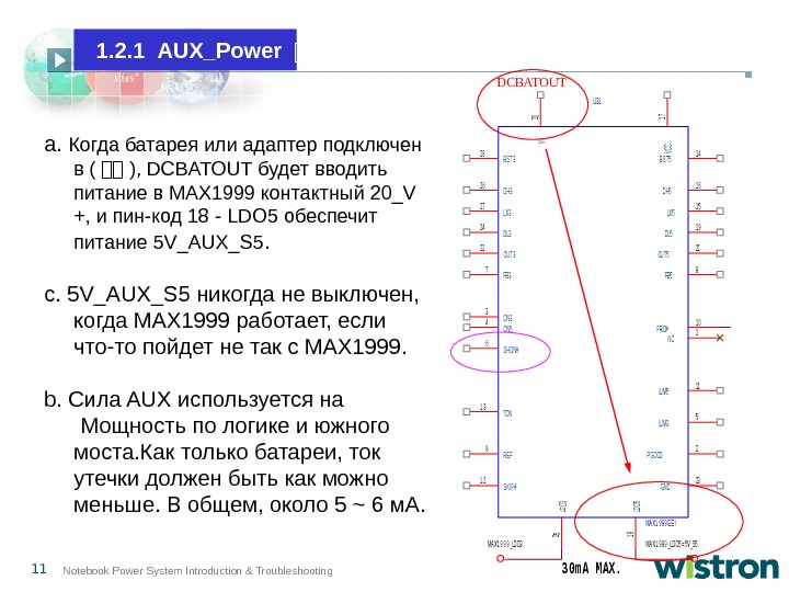
11 Notebook Power System Introduction & Troubleshooting. U 31 MA X 1 9 9 9 E E I 1 2 34 5 6 7 8 9 1 0 11 1 2 1 3 1 4 1 5 1 6 17 18 1 9 20 2122 23 24 25 26 27 28 NC P GOOD ON 3 ON 5 ILIM 3 S HDN# FB 3 RE F FB 5 P RO# ILIM 5 S K IP # TON B S T 5 LX 5 DH 5 VCC LDO 5 DL 5 V+ OU T 5 OUT 3 GND DL 3 LDO 3 DH 3 LX 3 B S T 3 MA X 1 9 9 9 _LDO 5 = 5 V _S 5 3 0 m A M AX. MA X 1 9 9 9 _LD O 3 DCBATOUT a. Когда батарея или адаптер подключен в ( 短短 ), DCBATOUT будет вводить питание в MAX 1999 контактный 20_V +, и пин-код 18 — LDO 5 обеспечит питание 5 V_AUX_S 5. c. 5 V_AUX_S 5 никогда не выключен, когда MAX 1999 работает, если что-то пойдет не так с MAX 1999. b. Сила AUX используется на Мощность по логике и южного моста. Как только батареи, ток утечки должен быть как можно меньше. В общем, около 5 ~ 6 м. А. 1. 2. 1 AUX_Power :
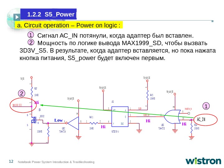
12 Notebook Power System Introduction & Troubleshooting Сигнал AC_IN потянули, когда адаптер был вставлен. Мощность по логике вывода MAX 1999_SD, чтобы вызвать 3 D 3 V_S 5. В результате, когда адаптер вставляется, но пока нажата кнопка питания, S 5_power будет включен первым. M 1 631 _E N GS D Q 51 2 N 70 0 21 2 3 5 V _A UX _S 5 1 0 0 K R 3 1 2 U 36 C T S A HCT 32 9 1 0 8 14 7 5 V _A UX _S 5 R 4 71 1 0 0 K R 3 1 2 5 V _A UX _S 5 5 V _S 5 AC_IN B L 3# R 267 1 0 K R 3 1 2 MA X 1 9 9 9 _S D_3 R 4 8 1 1 0 K R 3 12 R 31 4 1 0 0 K R 3 1 2 5 V _A UX _S 5 U 51 NC 7 S Z 0 8 -U 1 2 34 5 A B GNDY V CC U 50 C T S A HCT 1 4 56 14 7 P W RB T N_74 Hi. Hi Lowa. Circuit operation – Power on logic : 11 2 21. 2. 2 S 5_Power :
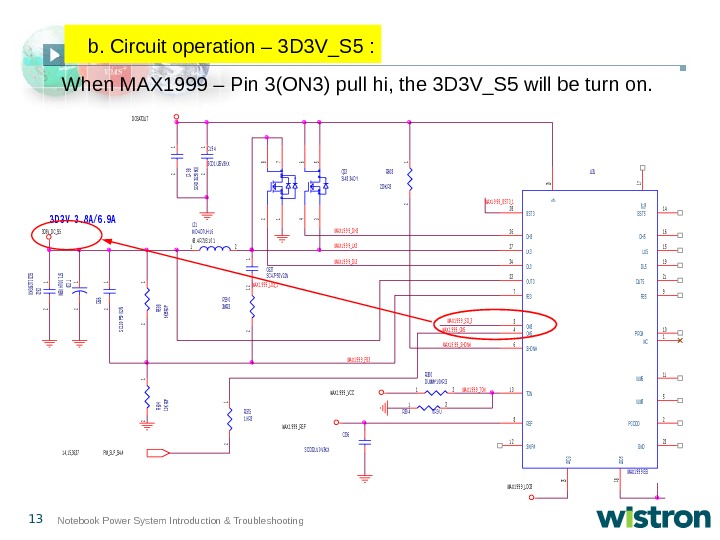
13 Notebook Power System Introduction & Troubleshooting. MA X 1 9 9 9 _LX 3_1 MA X 1 9 9 9 _LX 3 C 627 S C 4 7 P 50 V 2 JN 1 2 R 60 8 220 K R 3 1 2 PM_S LP _S 4 #1 4 , 1 5, 36, 37 MA X 1 9 9 9 _S HDN# R 30 0 DUMMY-1 0 K R 312 3 D 3 V _D C_S 5 MA X 1 9 9 9 _V C C MA X 1 9 9 9 _LDO 3 3 D 3 V 3. 8 A/6. 9 A R 30 40 R 3 -U 12 MA X 1 9 9 9 _DL 3 MA X 1 9 9 9 _ON 5 U 31 MA X 1 9 9 9 E E I 1 2 34 5 6 7 8 9 1 0 11 1 2 1 3 1 4 1 5 1 6 17 18 1 9 20 2122 23 24 25 26 27 28 NC P GOOD ON 3 ON 5 ILIM 3 S HDN # FB 3 RE F FB 5 P RO# ILIM 5 S K IP # TON B S T 5 LX 5 DH 5 VCC LDO 5 DL 5 V+ OUT 5 OUT 3 GN D DL 3 LDO 3 DH 3 LX 3 B S T 3 MA X 1 9 9 9 _S D_3 C 622 SCD 1 U 25 V 3 KX 1 2 MA X 1 9 9 9 _FB 3 R 59 02 MR 3 1 2 C 198 SC 4 D 7 U 25 V 6 KX 1 2 L 21 IND-4 D 7 UH-1 668. 4 R 71 B. 1 0 112 C 236 S CD 22 U 1 0 V 3 K X C 1 9 4 S CD 1 U 25 V 3 K X 1 2 MA X 1 9 9 9 _TON R 5751 K R 3 1 2 C 636 SC 100 P 50 V 2 JN 1 2 MA X 1 9 9 9 _DH 3 MA X 1 9 9 9 _B S T 3_1 DC B ATOUT MA X 1 9 9 9 _RE F R 60410 KR 3 F 1 2 Q 22 S I 4 8 34 DY 1 8 2 765 43 R 598 6 K 65 R 3 F 1 2 TC 30 ST 100 U 4 VBM 1 2 When MAX 1999 – Pin 3(ON 3) pull hi, the 3 D 3 V_S 5 will be turn on. b. Circuit operation – 3 D 3 V_S 5 :
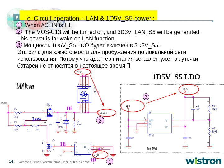
14 Notebook Power System Introduction & Troubleshooting When AC_IN is HI, The MOS-U 13 will be turned on, and 3 D 3 V_LAN_S 5 will be generated. This power is for wake on LAN function. Мощность 1 D 5 V_S 5 LDO будет включен в 3 D 3 V_S 5. Эта сила для южного моста для пробуждения по локальной сети использования. Потому что адаптер питания вставлен уже ток утечки батареи не относятся в настоящее время 短C 59 3 C 1 72 S C 20 P R 54 0 1 2 K 4 R 3 D 1 2 R 54 6 60 K 4 R 3 F 1 2 3 D 3 V _S 5 I ma x = 1 2 0 m. A 1 D 5 V _S 5 C 1 76 U 24 G 9 1 3 C-U 1 2 34 5 S HDN # GND INOU T S E T DCB ATOUTSSSG DDDDU 1 3 FDS 9 4 1 2 1234 5678 3 D 3 V _LA N_S 5 R 1 0 5 1 0 K R 3 12 LAN Power GS DQ 1 0 2 N 70 0 2 1 2 3 U 1 4 NC 7 S Z 32 -U 1234 5 ABGNDY V CC 3 D 3 V _S 5 B C 27 P M_S LP _S 3# R 1 0 11 K R 3 12 3 D 3 V _S 5 R 1 0 7 330 K R 3 12 R 9 5330 K R 3 1 2 D 3 RLZ 1 2 B 1 2 AC_IN Q 11 T P 0 61 0 T 12 3 1 D 5 V_S 5 LDO Hi. Hi Hi Low 1 2 123 3 c. Circuit operation – LAN & 1 D 5 V_S 5 power :
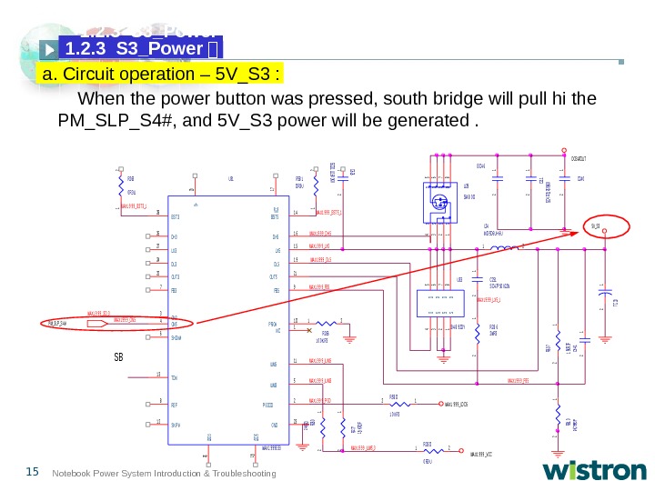
15 Notebook Power System Introduction & Troubleshooting When the power button was pressed, south bridge will pull hi the PM_SLP_S 4#, and 5 V_S 3 power will be generated. MA X 1 9 9 9 _V CC R 263 0 R 3 -U 1 2 C 626 SCD 1 U 16 V 3 KX 1 2 MA X 1 9 9 9 _ILIM 3 MA X 1 9 9 9 _ILIM 5 R 28 0 0 R 3 -U 12 MA X 1 9 9 9 _P GD R 28 62 MR 3 1 2 R 58 10 R 3 -U 1 2 MA X 1 9 9 9 _B S T 3_1 R 2661 0 0 K R 3 12 C 211 SC 4 D 7 U 25 V 6 KX 1 2 C 641 1 2 MA X 1 9 9 9 _LX 5_1 TC 33 1 2 MA X 1 9 9 9 _LDO 5 MA X 1 9 9 9 _ILIM 5_3 C 251 S C 4 7 P 50 V 2 JN 1 2 B C 4 61 2 SSSG DDDDU 29 S I 4 8 0 0 1234 5678 MA X 1 9 9 9 _S D_3 R 610 9 K 76 R 3 F 1 2 MA X 1 9 9 9 _DL 5 R 26024 KR 3 1 2 SB R 27718 KR 3 F 1 2 L 24 IND-5 D 6 UH-6 -U 12 U 31 MA X 1 9 9 9 E EI 1 2 34 5 6 7 8 9 1 0 11 1 2 1 3 1 4 1 5 1 6 17 18 1 9 20 2122 23 24 25 26 27 28 N C P GOOD ON 3 ON 5 ILIM 3 S HDN# FB 3 RE F FB 5 P R O# ILIM 5 S K IP # TON B S T 5 LX 5 DH 5 VCC LDO 5 DL 5 V+ OUT 5 OUT 3 GND DL 3 LDO 3 DH 3 LX 3 B S T 3 R 58 0 1 0 KR 3 12 R 60715 KR 3 F 1 2 D CB ATOUT C 24 0 1 2 U 33 S I 4 8 9 2 D Y 1234 8765 SSSG DDDD P M_S LP _S 4 # MA X 1 9 9 9 _B S T 5_1 MA X 1 9 9 9 _DH 5 MA X 1 9 9 9 _FB 5 5 V _S 3 MA X 1 9 9 9 _ON 5 MA X 1 9 9 9 _LX 5 MA X 1 9 9 9 _FB 5 1. 2. 3 S 3_Power : a. Circuit operation – 5 V_S 3 : 1. 2. 3 S 3_Power :
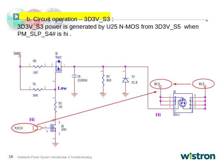
16 Notebook Power System Introduction & Troubleshooting 3 D 3 V_S 3 power is generated by U 25 N-MOS from 3 D 3 V_S 5 when PM_SLP_S 4# is hi. C 28 1 S CD 1 U 50 V 5 K X GS D Q 53 2 N 70 0 2 1 2 3 Q 32 T P 0 61 0 T 12 3 3 D 3 V _S 5 R 31 5 1 K R 3 1 2 3 D 3 V _S 3 S S S GD D U 25 FDS 9 4 1 2 3 45 6 7 8 R 30 5 1 0 K R 3 12 DCB ATOUT R 30 2 330 K R 3 1 2 P M_S LP _S 4 # D 1 9 RLZ 1 2 B 1 2 R 311 330 K R 3 12 Hi Hi. Lowb. Circuit operation – 3 D 3 V_S 3 :
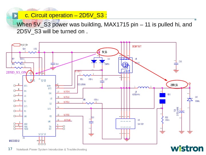
17 Notebook Power System Introduction & Troubleshooting When 5 V_S 3 power was building, MAX 1715 pin – 11 is pulled hi, and 2 D 5 V_S 3 will be turned on. M 1 71 5 B S T 2 R 59 10 R 3 -0 -U 12 D 4 5 S S M 24 L 2 1 C 20 81 2 R 58 20 R 3 -0 -U 12 P M_S LP _S 3# 2 D 5 V_S 3 M 1 71 5 LX 2 R 24 91 0 R 312 SSSG DDDDU 65 S I 4 8 0 0 1234 5678 R 5770 R 3 -0 -U 12 R 5550 R 3 -0 -U 12 C 20 7 S CD 1 U 25 V 3 K X 1 2 M 1 71 5 DL 2 U 61 MAX 1715 EEI- U 2 1 2 3 4 5 6 7 8 9 1011 1 2 1 3 1 4 28 27 26 25 24 23 22 2120 1 9 1 8 1 7 1 6 15 OUT 1 FB 1 ILIM 1 V+ TON S K IP # P GOOD A GND RE F ON 1 ON 2 ILIM 2 FB 2 OUT 2 N. C. LX 1 DH 1 B S T 1 DL 1 N. C. P GND VCCVDD DL 2 B S T 2 DH 2 LX 2 N. C. TC 32 ST 220 U 4 VDM-61 2 C 1 9 11 2 C 21 3 D 1 0 B AW 56 -1 12 3 R 59 3 1 2 L 25 IND-5 D 6 UH-6 -U 12 5 V_S 3 M 1 71 5 DH 2 M 1 71 5 ILIM 2 M 1 71 5 FB 2 DCBAT OUT R 59 20 R 3 -0 -U 1 2 U 69 S I 4 8 9 2 DY 1234 8765 SSSG DDDD 2 D 5 D_S 3_ON c. Circuit operation – 2 D 5 V_S 3 :
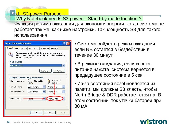
18 Notebook Power System Introduction & Troubleshooting Функция режима ожидания для экономии энергии, когда система не работает так же, как ниже настройки. Так, мощность S 3 для такого использования. • Система войдет в режим ожидания, если NB остается в бездействии в течение 30 минут. • В режиме ожидания, если кнопка питания нажата, система вернется в предыдущее состояние в 5 сек. • Из-за состояния возобновляется из памяти, мы должны S 3 власть, чтобы North Bridge & DDR работает стоя на. В этом состоянии, ток утечки батареи при 30 м. А. Why Notebook needs S 3 power – Stand-by mode function ? d. S 3 power Purpose :
19 Notebook Power System Introduction & Troubleshooting After PM_SLP_S 4# signal was generated for a few sec , the South Bridge will output PM_SLP_S 3# on hi level, and 1 D 5 V_S 0 will be turned on. M 1 71 5 LX 1 U 61 MAX 1 715 EEI- U 2 1 2 3 4 5 6 7 8 9 1011 1 2 1 3 1 4 28 27 26 25 24 23 22 2120 1 9 1 8 1 7 1 6 15 OUT 1 FB 1 ILIM 1 V+ TON S K IP # P GOOD A GND RE F ON 1 ON 2 ILIM 2 FB 2 OUT 2 N. C. LX 1 DH 1 B S T 1 DL 1 N. C. P GND VCCVDD DL 2 B S T 2 DH 2 LX 2 N. C. R 5770 R 3 -0 -U 12 M 1 71 5 DH 1 R 5530 R 3 -0 -U 12 M 1 71 5 ILIM 1 D 11 S S M 24 L 2 1 M 1 71 5 DH 1 _1 M 1 71 5 DL 1 R 24 91 0 R 312 R 5565 K 1 R 3 F 1 2 PM_SLP_S 3# C 1 8 9 1 2 M 1 71 5 FB 1 C 61 0 S C 1 U 1 0 V 3 Z Y L 23 IND-4 D 7 UH-1 6 12 T C 31 S T 1 0 0 U 4 V B M 1 2 DCB ATOUT R 558 30 0 K R 312 R 5540 R 3 -0 -U 12 U 62 S I 4 8 34 DY 1 8 2 765 43 C 1 8 8 S CD 1 U 25 V 3 K X 1 2 R 54 91 0 K R 3 F 1 2 C 21 0 1 2 M 1 71 5 DL 1 _1 R 58 20 R 3 -0 -U 12 1 D 5 V_S 0 a. Circuit operation – 1 D 5 V_S 0 : 1. 2. 3 S 0_Power :
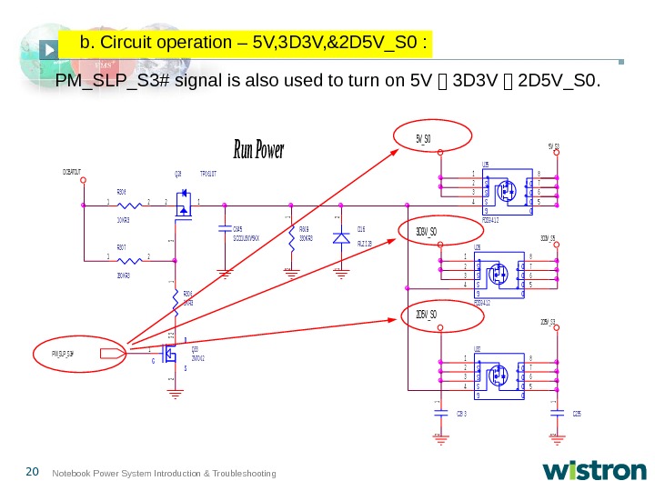
20 Notebook Power System Introduction & Troubleshooting PM_SLP_S 3# signal is also used to turn on 5 V 短 3 D 3 V 短 2 D 5 V_S 0. S S S GD D U 35 FDS 9 4 1 2 3 45 6 7 8 5 V_S 0 R 30 7 330 K R 3 12 2 D 5 V_S 0 C 64 5 S CD 1 U 50 V 5 K X 2 D 5 V _S 3 P M_S LP _S 3# R 30 8 1 0 K R 3 12 C 28 3 1 2 GS DQ 33 2 N 70 0 2 1 2 3 DCB ATOUT 3 D 3 V_S 0 S S S GD D U 26 FDS 9 4 1 2 3 45 6 7 8 S S S GD D U 32 1 2 3 45 6 7 8 D 1 6 RLZ 1 2 B 1 2 3 D 3 V _S 5 5 V _S 3 R 30 6 1 K R 3 1 2 R 60 9 330 K R 3 1 2 C 235 1 2 Run Power Q 28 T P 0 61 0 T 12 3 b. Circuit operation – 5 V, 3 D 3 V, &2 D 5 V_S 0 :
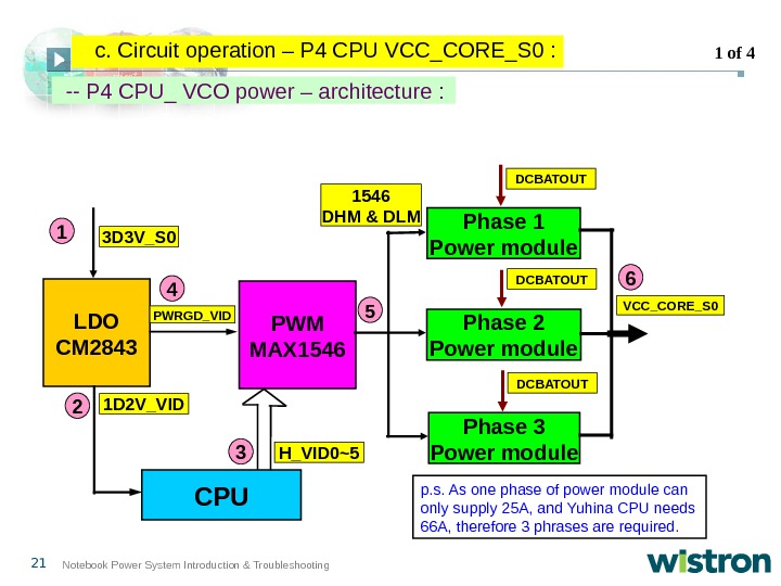
21 Notebook Power System Introduction & Troubleshooting — P 4 CPU_ VCO power – architecture : PWM MAX 1546 CPULDO CM 2843 Phase 1 Power module Phase 2 Power module Phase 3 Power module 3 D 3 V_S 0 1 D 2 V_VID H_VID 0~5 DCBATOUT VCC_CORE_S 0 PWRGD_VID 1 54 32 1546 DHM & DLM 6 p. s. As one phase of power module can only supply 25 A, and Yuhina CPU needs 66 A, therefore 3 phrases are required. 1 of 4 c. Circuit operation – P 4 CPU VCC_CORE_S 0 :
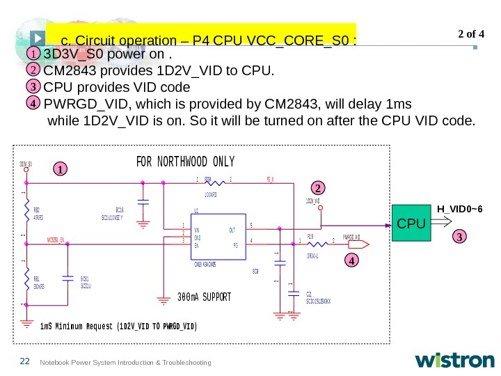
22 Notebook Power System Introduction & Troubleshooting 3 D 3 V_S 0 power on. CM 2843 provides 1 D 2 V_VID to CPU provides VID code PWRGD_VID, which is provided by CM 2843, will delay 1 ms while 1 D 2 V_VID is on. So it will be turned on after the CPU VID code. R 1 9 0 R 3 -0 -U 12 R 334 1 0 0 K R 3 12 B CB 1 S CD 1 U P W RGD_V ID FOR NORT HWOOD ONLY 3 D 3 V _S 0 C 21 S CD 0 1 5 U 25 V 3 K X 1 2 FS _X U 1 CM 28 4 3 A CIM 25 1 2 34 5 V IN GND E NP G OUT B C 9 1 2 1 D 2 V _V ID MIC 5258 _E N 30 0 m. A SU PPORT 1 m S Mi ni m u m Re q u e st (1 D 2 V_VI D T O PWRGD_VI D) RB 2 4 7 K R 3 1 2 B C 1 6 S C 1 U 1 0 V 3 Z Y RB 1 330 K R 3 1 21 1 2 42 4 3 3 CPU H_VID 0~6 2 of 4 c. Circuit operation – P 4 CPU VCC_CORE_S 0 :
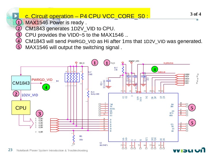
23 Notebook Power System Introduction & Troubleshooting 1 54 6 DHS 32 3 D 3 V _S 0 R 1 8 71 0 R 3 1 2 5 V _S 0 P M_DP RS LP V R# RN 9 S RN 1 0 K -21234 5678 R 631 0 R 3 -U 1 2 P W RGD_V ID BC 84 SC 1 U 10 V 3 KX 1 2 H_V ID 15 R 1 4 71 0 K R 2 1 2 DCB ATOUT _V CP U H_V ID 25 1 54 6 CS -32 R 1 4 8 Dummy-1 0 K R 2 1 54 6 CS +32 C 127 SC 1 U 10 V 3 ZY H_V ID 05 1 54 6 CM-32 C 519 SC 470 P 50 V 3 JN H_V ID 35 H_V ID 45 H_V ID 54 C 137 SC 1 U 25 V-U 1 21 54 6 CM+32 U 21 MA X 1 54 6 E T L 123 45 6 78 9 10 11 1 2 13 1 4 1516 201 9 18 17 30 2928 272625 24232221 4039383736 35 34 33 32 3141 T IMETONMUX S E L S 0 S 1 SHDN# OFSRE F ILIM VCC GND CCV GNDS CCI FBOAIN- D 4 D 5 SKIP# OAIN+ VDD DLMDHM LX MB S T MV ROK D 0 D 1 D 2 D 3 CSPCSNCMNCMPV+ BSTS LX S DHS DLS PGNDGND 4 53 5112 1 MAX 1546 Power is ready. CM 1843 generates 1 D 2 V_VID to CPU provides the VID 0~5 to the MAX 1546. . CM 1843 will send PWRGD_VID as Hi after 1 ms that 1 D 2 V_VID was generated. MAX 1546 will output the switching signal. 4 5 CM 1843 CPU 4 PWRGD_VID 2 1 D 2 V_VID 3 3 of 4 c. Circuit operation – P 4 CPU VCC_CORE_S 0 :
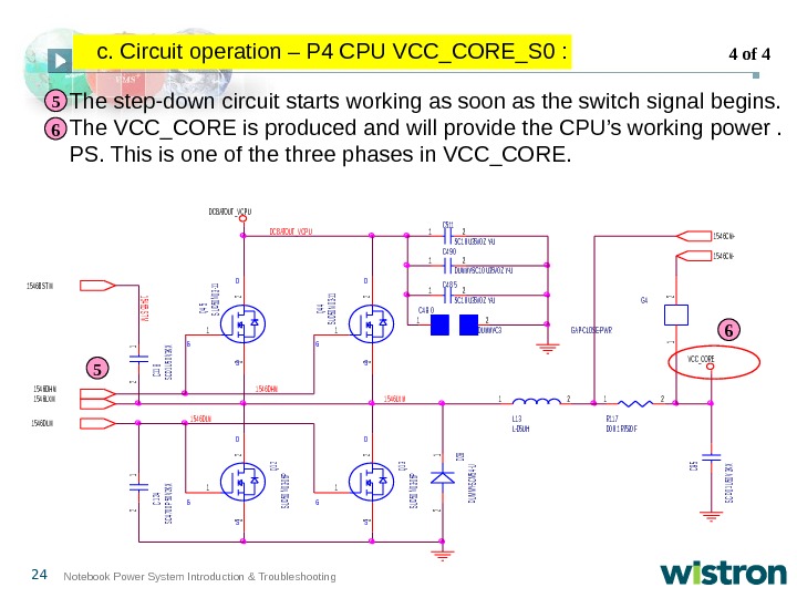
24 Notebook Power System Introduction & Troubleshooting 1 54 6 DHM G S D Q 12 SUD 50 N 03 -06 P 1 3 2 C 118 SCD 1 U 50 V 3 KX 1 2 C 4 8 0 DUMMY-C 312 G S D Q 44 SUD 50 N 03 -11 1 3 2 C 124 SC 4700 P 50 V 2 KX 1 2 1 54 6 DHM R 11 7 D 0 0 1 R 7520 F 12 G 4 GA P -CLOS E -P W R 1 2 C 95 SCD 01 U 50 V 3 KX V CC_CORE 1 54 6 DLM G S D Q 45 SUD 50 N 03 -11 1 3 2 C 4 8 5 S C 1 0 U 35 V 0 Z Y-U 12 1 54 6 CM+ DCB ATOUT _V CP U 1 54 6 LX M 1546 BSTM C 4 9 0 DUMMY-S C 1 0 U 35 V 0 Z Y-U 12 DCB ATOUT _V CP U L 1 3 L-D 5 UH 12 C 511 S C 1 0 U 35 V 0 Z Y-U 12 1 54 6 DLM 1 54 6 CM- 1 54 6 B S T M D 28 DUMMY-SCM 54 -U 2 1 G S D Q 13 SUD 50 N 03 -06 P 1 3 2 The step-down circuit starts working as soon as the switch signal begins. The VCC_CORE is produced and will provide the CPU’s working power. PS. This is one of the three phases in VCC_CORE. 5 65 6 4 of 4 c. Circuit operation – P 4 CPU VCC_CORE_S 0 :
25 Notebook Power System Introduction & Troubleshooting PWM MAX 1546 ISL 6218 CPULDO CM 2843 Phase 1 Power module Phase 2 Power module Phase 3 Power module 3 D 3 V_S 0 1 D 2 V_VID H_VID 0~5 DCBATOUT VCC_CORE_S 0 PWRGD_VID 1 54 32 1546 DHM & DLM 61 D 2 V_S 0 VCC_IO_S 0(1. 05 V) CPUCORE_ON Banias CPU needs 21 A, so only one phase is needed. The power system can separate two kinds of architecture for CPU. But the only difference between P 4 and Banias CPU power architecture is VCC_COER_S 0. Such as below : d. P 4 & Banias CPU VCC_CORE_S 0 difference :
26 Notebook Power System Introduction & Troubleshooting By now we have learned how NB power is generated and why it must be done in a specific sequence. You might start to wonder, “What is other Power application? ” In the following section, I will show you the power consumption of all devices in a NB. You will learn: 2. 1 Power budget block diagram 2. 2 NB power application 2. 3 Multi–power device 2. Power plan introduction :
27 Notebook Power System Introduction & Troubleshooting Create a NB power system with fixed procedure, so we can know the power budget of all devices from the power plan procedure. Design procedure : a. Power budget : b. Power application : We must first know the power category and consumption of all devices, and then we can start to define the SPEC of power. After power SPEC was defined, we need to confirm the timing & sequence when power is turned on. And separate them with S 5, S 3, S 0, etc. for the purpose of power saving. 2. Power plan introduction : (cont’d)
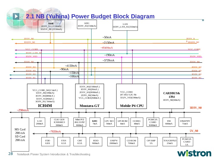
28 Notebook Power System Introduction & Troubleshooting 1 D 25 V_S 0 VCC_CORE_S 0(2. 5 m. A ) 1 D 5 V_S 0(599 m. A) 3 D 3 V_S 0(480 m. A ) 1 D 5 V_S 5(90 m. A ) 3 D 3 V_S 5( 166 m. A) ICH 4 MVCC_CORE 1 D 5 V_S 0(3140 m. A ) 3 D 3 V_S 0(20 m. A ) 2 D 5 V_S 3(2000 m. A ) 2 D 5 V_S 0(50 m. A) VCC_CORE(940 m. A ) Montara-GT Mobile P 4 CPU 3 D 3 V_S 3 VCC_CORE (67. 4 A)-3. 2 G Hz 1 D 2 V_VID(190 m. A) CLK GEN ICS 950813 360 m. A CARDBUS& 1394 3 D 3 V_S 0(60 m. A) CODEC 40 m. ALPC SIO 50 m. A LPCROM 6 m. ADDR 2 D 5 V_S 3 (2150 m. A) 1 D 25 V_S 0 (2150 m. A) KBC 7 m. A~150 m. A ~2150 m. A ~190 m. A PCMCIA CARD 1000 m. A 2 D 5 V_S 3 ~4150 m. A ~65400 m. A Mini PCI 802. 11/BT 660 m. A 1 D 25 V_S 0 VCC_CORE 1 D 2 V_VID 3 D 3 V_S 3 3 D 3 V_S 5 2 D 5 V_S 3 3 D 3 V_S 5~50 m. A ~7650 m. A ~166 m. A 3 D 3 V_S 0 5 V_S 0 CRT 0. 5 A HDD 900 m. A CD ROM 700 m. A OP AMP 1 A TOUCHPAD 25 m. A PCMCIA CARD 1 A 1394 -PHY 71 m. A 2 D 5 V_S 0 FIR 600 m. ALCD 200 m. A~2984 m. A 1 D 2 V_VID 1 D 5 V_S 0 ~3739 m. A FAN 0. 5 AMS Card 200 m. A SD Card 200 m. A USB*4 2000 m. A 1 D 5 V_S 02 D 5 V_S 0 KBC 3 D 3 V_S 3(150 m. A) LAN 3 D 3 V_LAN_S 5(150 m. A) 1 D 5 V_S 5 ~90 m. A 3 D 3 V_LAN_S 5 FDD 0. 8 A 2. 1 NB (Yuhina) Power Budget Block Diagram
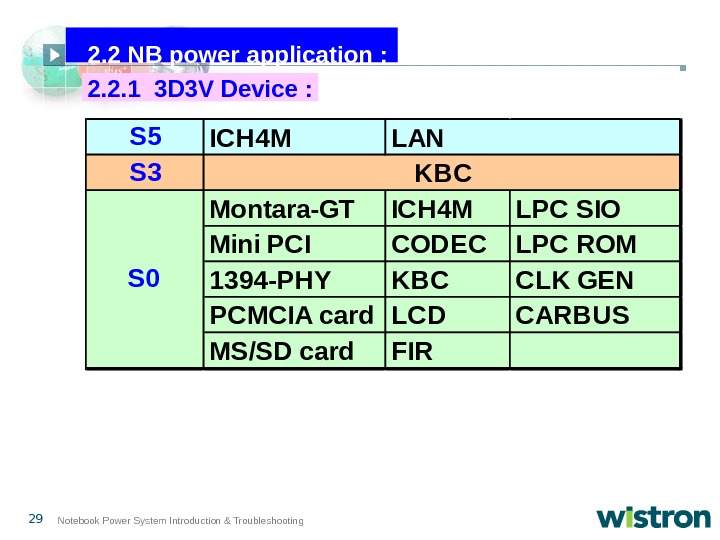
29 Notebook Power System Introduction & Troubleshooting. S 5 ICH 4 M S 3 Montara-GTICH 4 MLPC SIO Mini PCICODECLPC ROM 1394 -PHYKBCCLK GEN PCMCIA card. LCDCARBUS MS/SD card. FIR S 0 KBC LAN 2. 2. 1 3 D 3 V Device : 2. 2 NB power application :
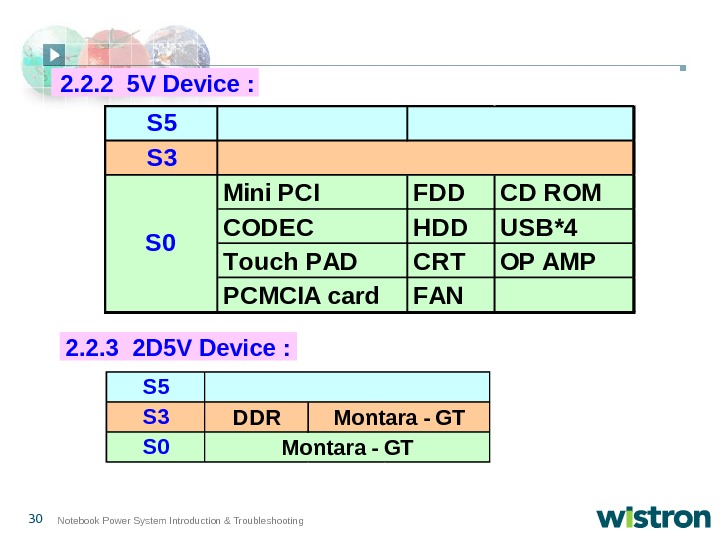
30 Notebook Power System Introduction & Troubleshooting. S 5 S 3 Mini PCIFDDCD ROM CODECHDDUSB*4 Touch PADCRTOP AMP PCMCIA card. FAN S 0 2. 2. 3 2 D 5 V Device : S 5 S 3 DDR S 0 Montara — GT 2. 2. 2 5 V Device :
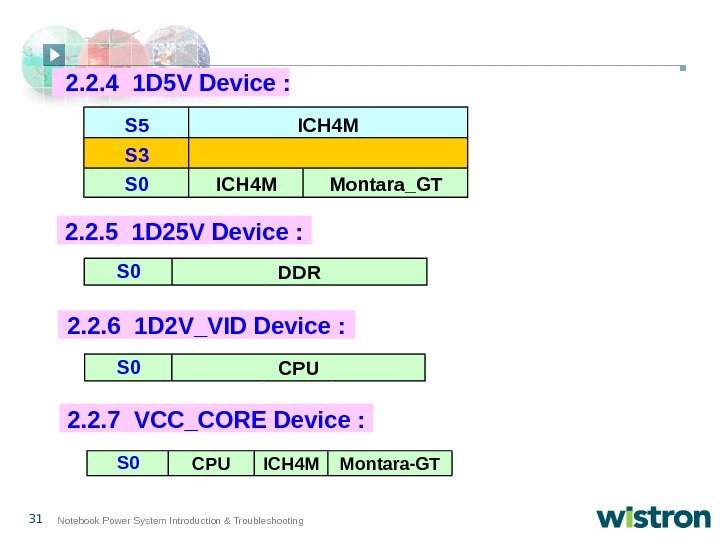
31 Notebook Power System Introduction & Troubleshooting 2. 2. 6 1 D 2 V_VID Device : 2. 2. 5 1 D 25 V Device : S 0 DDR S 0 CPU ICH 4 M Montara-GT 2. 2. 7 VCC_CORE Device : S 5 S 3 S 0 ICH 4 M Montara_GTICH 4 M 2. 2. 4 1 D 5 V Device :
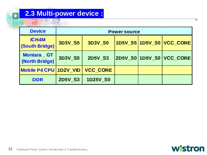
32 Notebook Power System Introduction & Troubleshooting Device ICH 4 M (South Bridge) 3 D 3 V_S 5 3 D 3 V_S 0 1 D 5 V_S 5 1 D 5 V_S 0 VCC_CORE Montara _ GT (North Bridge) 3 D 3 V_S 0 2 D 5 V_S 3 2 D 5 V_S 0 1 D 5 V_S 0 VCC_CORE Mobile P 4 CPU 1 D 2 V_VID VCC_CORE DDR 2 D 5 V_S 3 1 D 25 V_S 0 Power source 2. 3 Multi-power device :
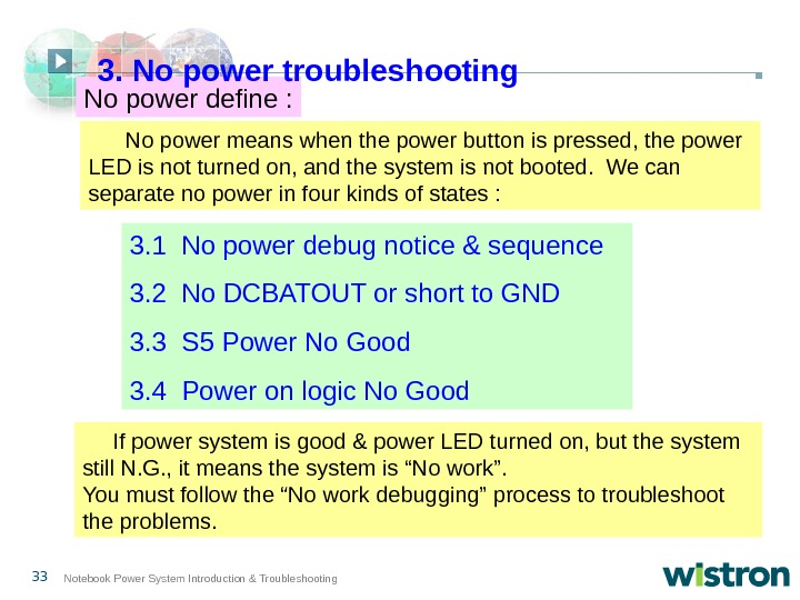
33 Notebook Power System Introduction & Troubleshooting No power means when the power button is pressed, the power LED is not turned on, and the system is not booted. We can separate no power in four kinds of states : 3. 1 No power debug notice & sequence 3. 2 No DCBATOUT or short to GND 3. 3 S 5 Power No Good 3. 4 Power on logic No Good. No power define : If power system is good & power LED turned on, but the system still N. G. , it means the system is “No work”. You must follow the “No work debugging” process to troubleshoot the problems. 3. No power troubleshooting
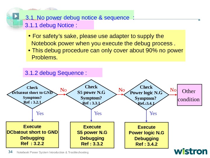
34 Notebook Power System Introduction & Troubleshooting 3. 1. 1 debug Notice : • For safety’s sake, please use adapter to supply the Notebook power when you execute the debug process. • This debug procedure can only cover about 90% no power Problems. 3. 1. 2 debug Sequence : Check Dcbatout short to GND Symptom? Ref : 3. 2. 1 Check S 5 power N. G Symptom? Ref : 3. 3. 1 Check Power logic N. G Symptom? Ref. : 3. 4. 1 Execute DCbatout short to GND Debugging Ref : 3. 2. 2 Execute S 5 power N. G Debugging Ref : 3. 3. 2 Execute Power logic N. G Debugging Ref : 3. 4. 2 Other condition No No Yes Yes 3. 1 No power debug notice & sequence :
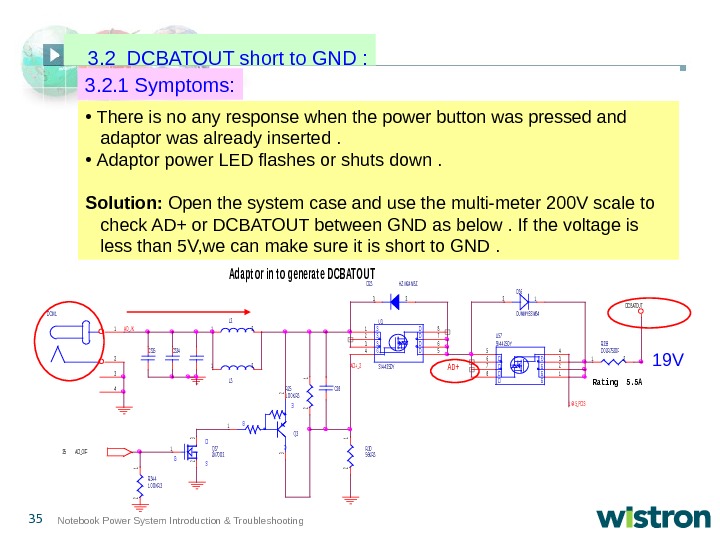
35 Notebook Power System Introduction & Troubleshooting 3. 2. 1 Symptoms: • There is no any response when the power button was pressed and adaptor was already inserted. • Adaptor power LED flashes or shuts down. Solution: Open the system case and use the multi-meter 200 V scale to check AD+ or DCBATOUT between GND as below. If the voltage is less than 5 V, we can make sure it is short to GND. DC B ATOUT Ad a p t o r in t o g e ne rat e D CB AT O U T Rati ng 5. 5 A AD+ A D_JK A D+ _2 1 64 5_P DS D 23 HZ M 24 NB Z 23 C 28 L 212 GS DQ 372 N 70 0 21 2 3 R 251 0 0 K R 3 1 2 R 34 41 0 0 K R 3 1 2 DC IN 1 1 2 3 4 L 3 12 SSGDDDDSU 3 S I 4 4 25 DY 12345678 R 3056 K R 3 1 2 C 334 C 335 C B E Q 3 3 1 2 D 36 DUMMY-S S M 34 21 R 259 D 0 2 R 7520 F 12 SSGDDDDS U 57 S I 4 4 25 DY 12345678 A D_OFF 25 19 V 3. 2 DCBATOUT short to GND :
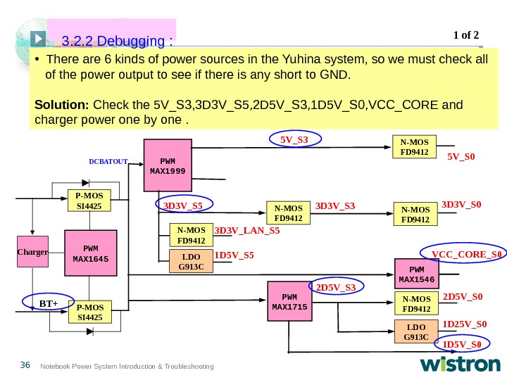
36 Notebook Power System Introduction & Troubleshooting • There are 6 kinds of power sources in the Yuhina system, so we must check all of the power output to see if there is any short to GND. Solution: Check the 5 V_S 3, 3 D 3 V_S 5, 2 D 5 V_S 3, 1 D 5 V_S 0, VCC_CORE and charger power one by one. PWM MAX 1645 Charger P-MOS SI 4425 PWM MAX 1999 PWM MAX 1715 N-MOS FD 9412 3 D 3 V_S 5 N-MOS FD 9412 LDO G 913 C 5 V_S 3 3 D 3 V_S 0 3 D 3 V_LAN_S 5 1 D 5 V_S 5 2 D 5 V_S 3 2 D 5 V_S 0 LDO G 913 C 1 D 25 V_S 0 PWM MAX 1546 1 D 5 V_S 0 BT+ DCBATOUT VCC_CORE_S 0 5 V_S 0 1 of 2 3. 2. 2 Debugging :
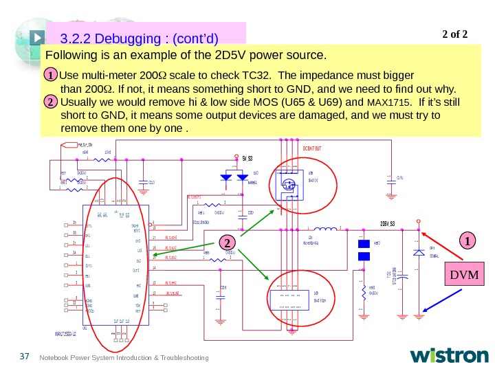
37 Notebook Power System Introduction & Troubleshooting Following is an example of the 2 D 5 V power source. Use multi-meter 200 scale to check TC 32. The impedance must bigger than 200 . If not, it means something short to GND , and we need to find out why. Usually we would remove hi & low side MOS (U 65 & U 69) and MAX 1715. If it’s still short to GND, it means some output devices are damaged, and we must try to remove them one by one. M 1 71 5 B S T 2 R 59 10 R 3 -0 -U 12 D 4 5 S S M 24 L 2 1 C 20 81 2 R 58 20 R 3 -0 -U 12 P M_S LP _S 3# 2 D 5 V_S 3 M 1 71 5 LX 2 R 24 91 0 R 312 SSSG DDDDU 65 S I 4 8 0 0 1234 5678 R 5770 R 3 -0 -U 12 R 5550 R 3 -0 -U 12 C 20 7 S CD 1 U 25 V 3 K X 1 2 M 1 71 5 DL 2 U 61 MAX 1715 EEI- U 2 1 2 3 4 5 6 7 8 9 1011 1 2 1 3 1 4 28 27 26 25 24 23 22 2120 1 9 1 8 1 7 1 6 15 OUT 1 FB 1 ILIM 1 V+ TON S K IP # P GOOD A GND RE F ON 1 ON 2 ILIM 2 FB 2 OUT 2 N. C. LX 1 DH 1 B S T 1 DL 1 N. C. P GND VCCVDD DL 2 B S T 2 DH 2 LX 2 N. C. TC 32 ST 220 U 4 VDM-61 2 C 1 9 11 2 C 21 3 D 1 0 B AW 56 -1 12 3 R 59 3 1 2 L 25 IND-5 D 6 UH-6 -U 12 5 V_S 3 M 1 71 5 DH 2 M 1 71 5 ILIM 2 M 1 71 5 FB 2 DCBAT OUT R 59 20 R 3 -0 -U 1 2 U 69 S I 4 8 9 2 DY 1234 8765 SSSG DDDD DVM 1 2 2 12 of 2 3. 2. 2 Debugging : (cont’d)
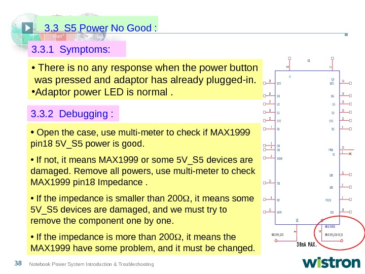
38 Notebook Power System Introduction & Troubleshooting 3. 3. 1 Symptoms: U 31 MA X 1 9 9 9 E E I 1 2 34 5 6 7 8 9 1 0 11 1 2 1 3 1 4 1 5 1 6 17 18 1 9 20 2122 23 24 25 26 27 28 NC P GOOD ON 3 ON 5 ILIM 3 S HDN# FB 3 RE F FB 5 P RO# ILIM 5 S K IP # TON B S T 5 LX 5 DH 5 VCC LDO 5 DL 5 V+ OUT 5 OUT 3 GND DL 3 LDO 3 DH 3 LX 3 B S T 3 MA X 1 9 9 9 _LDO 5 = 5 V _S 5 3 0 m A M AX. MA X 1 9 9 9 _LDO 3 • There is no any response when the power button was pressed and adaptor has already plugged-in. • Adaptor power LED is normal. 3. 3. 2 Debugging : • Open the case, use multi-meter to check if MAX 1999 pin 18 5 V_S 5 power is good. • If not, it means MAX 1999 or some 5 V_S 5 devices are damaged. Remove all powers, u se multi-meter to check MAX 1999 pin 18 Impedance. • If the impedance is smaller than 200 , it means some 5 V_S 5 devices are damaged, and we must try to remove the component one by one. • If the impedance is more than 200 , it means the MAX 1999 have some problem, and it must be changed. 3. 3 S 5 Power No Good :
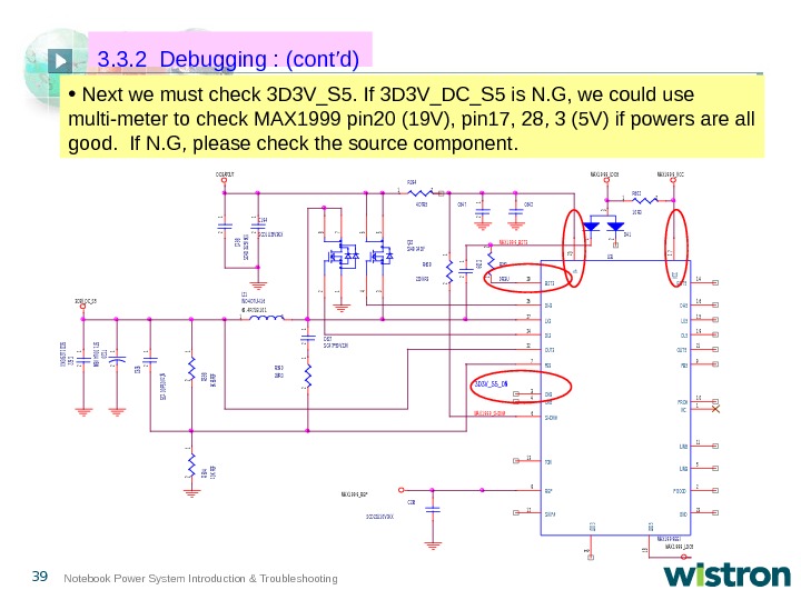
39 Notebook Power System Introduction & Troubleshooting • Next we must check 3 D 3 V_S 5. If 3 D 3 V_DC_S 5 is N. G, we could use multi-meter to check MAX 1999 pin 20 (19 V), pin 17, 28, 3 (5 V) if powers are all good. If N. G, please check the source component. MA X 1 9 9 9 _RE F DCB ATOUT 3 D 3 V _DC_S 5 MA X 1 9 9 9 _LDO 5 MA X 1 9 9 9 _V CC MA X 1 9 9 9 _LDO 5 3 D 3 V_S 5_ON MA X 1 9 9 9 _B S T 3 MA X 1 9 9 9 _S HDN# C 64 2 C 2091 2 R 60 2 1 0 R 3 12 C 236 S CD 22 U 1 0 V 3 K X R 60 8 220 K R 3 1 2 R 59 02 MR 3 1 2 R 263 0 R 3 -U 1 2 C 64 71 2 R 598 6 K 65 R 3 F 1 2 R 60410 KR 3 F 1 2 TC 30 ST 100 U 4 VBM 1 2 C 622 SCD 1 U 25 V 3 KX 1 2 Q 22 S I 4 8 34 DY 1 8 2 765 43 C 198 SC 4 D 7 U 25 V 6 KX 1 2 C 636 SC 100 P 50 V 2 JN 1 2 C 1 9 4 S CD 1 U 25 V 3 K X 1 2 C 627 S C 4 7 P 50 V 2 JN 1 2 D 4 112 3 R 29 4 4 D 7 R 5 12 U 31 MA X 1 9 9 9 E E I NC 1 P GOOD 2 ON 33 ON 54 ILIM 35 S HDN#6 FB 37 RE F 8 FB 59 P RO#1 0 ILIM 511 S K IP #1 2 TON 1 3 B S T 51 4 LX 51 5 DH 51 6 VCC 17 LDO 5 18 DL 51 9 V+ 20 OUT 521 OUT 322 GND 23 DL 324 LDO 3 25 DH 326 LX 327 B S T 328 L 21 IND-4 D 7 UH-1 668. 4 R 71 B. 1 0 112 3. 3. 2 Debugging : (cont’d)
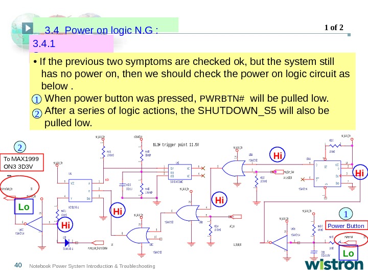
40 Notebook Power System Introduction & Troubleshooting 3. 4. 1 Symptom : • If the previous two symptoms are checked ok, but the system still has no power on, then we should check the power on logic circuit as below. When power button was pressed, PWRBTN# will be pulled low. After a series of logic actions, the SHUTDOWN_S 5 will also be pulled low. 5 V _A UX _S 5 DCB ATOUT 5 V _A UX _S 5 5 V _A UX _S 5 BL 3# trigge r poin t 11. 5 V B L 3# U 50 B T S A HCT 1 4 34 14 7 U 36 A T S A HCT 321 23 14 7 R 4 73 1 K R 3 12 R 4 8 04 7 K R 3 1 2 C 521 S CD 1 U 1 6 V B C 8 3 S CD 1 U U 51 NC 7 S Z 0 8 -U A 1 B 2 GND 3 Y 4 V CC 5 U 52 S -8 0 8 4 0 CNMC OUT 1 V DD 2 V S S 3 NC 5 NC 4 R 31 31 0 0 K R 3 1 2 R 31 41 0 0 K R 3 1 2 R 31 0 K R 3 12 R 4 711 0 0 K R 3 1 2 U 50 CT S A HCT 1 4 56 14 7 D 29 S 1 N 4 1 4 8 -U 12 R 4 8 11 0 K R 3 1 2 R 4 6933 K R 3 F 1 2 R 4 681 7 K 4 R 3 F 1 2 U 34 A T S A HCT 74 D 2 CLK 3 Q 5 Q 6 V CC 1 4 PR 4 GND 7 CL 1 U 36 BT S A HCT 32 4 56 14 7 U 36 C T S A HCT 32 9 1 08 14 7 P WRB T N#25 P M_S LP _S 4 # 1 4 , 1 5, 33, 36 S HUT DOW N_S 533 P URE _HW_S HUT DOW N#1 6 A C_IN 11 , 25, 36 Lo Hi Hi Hi. Lo. To MAX 1999 ON 3 3 D 3 V Power Button 1 12 2 1 of 2 3. 4 Power on logic N. G :
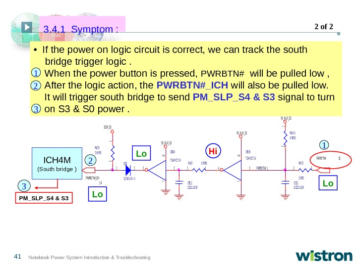
41 Notebook Power System Introduction & Troubleshooting • If the power on logic circuit is correct, we can track the south bridge trigger logic. When the power button is pressed, PWRBTN# will be pulled low , After the logic action, the PWRBTN#_ICH will also be pulled low. It will trigger south bridge to send PM_SLP_S 4 & S 3 signal to turn on S 3 & S 0 power. Lo Lo Hi 3 D 3 V _S 5 5 V _A UX _S 5 P WRB T N#_1 U 50 A T S A HCT 1 4 12 14 7 U 50 B T S A HCT 1 4 34 14 7 R 4 73 1 K R 3 12 R 4 8 04 7 K R 3 1 2 R 4 674 7 K R 312 C 521 S CD 1 U 1 6 VC 51 2 S CD 1 U 1 6 V R 4 791 0 K R 3 1 2 D 30 S 1 N 4 1 4 8 -U 12 P W RB T N#_ICH 1 4 P W RB T N#25 ICH 4 M (South bridge ) PM_SLP_S 4 & S 3 1 12 2 3 3 2 of 2 3. 4. 1 Symptom :
42 Notebook Power System Introduction & Troubleshooting 3. 4. 2 Debugging : • If SHUTDOWN_S 5 is not pulled low, it means some logic ICs or components during this path are N. G. . If it is the case, then just follow the circuit to find out the problems, and replace them. • If the PWRBTN#_ICH is not pulled low, it means some logic ICs or components during this path are N. G. If it is the case, then just follow the circuit to find out the problems, and replace them. • If the PM_SLP_S 4 & S 3 is not pulled hi, maybe the south bridge is damaged. 3. No Power Debug